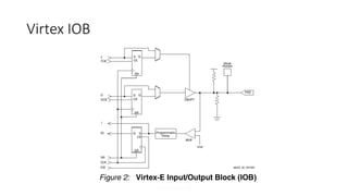
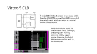
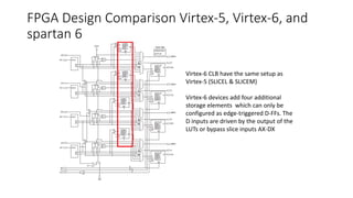
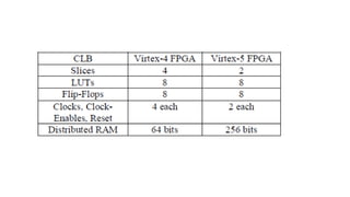
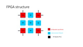
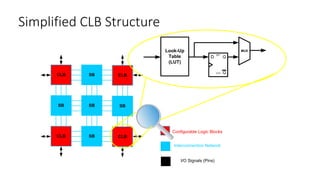
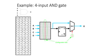
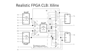
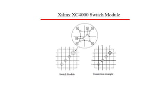
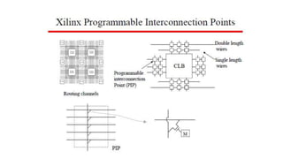
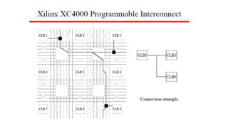
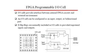
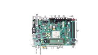
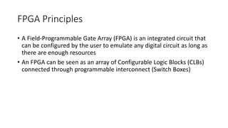
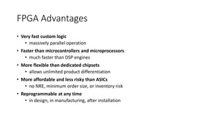
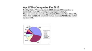
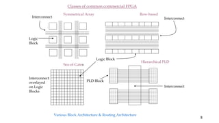
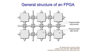
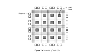
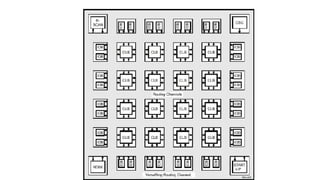
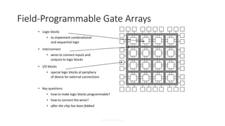
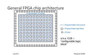
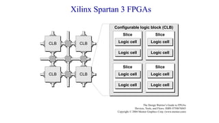
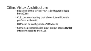
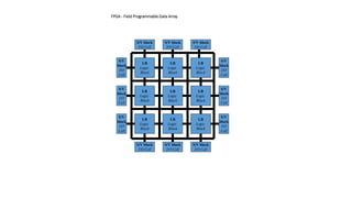
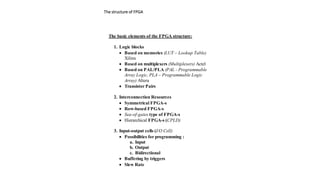
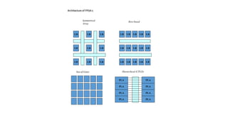
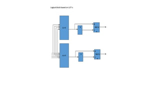
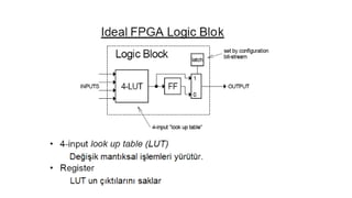
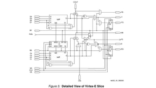
FPGAs have programmable logic blocks and interconnects that can be configured to implement any digital circuit. The two major FPGA manufacturers are Xilinx and Altera, who together make up 89% of the market. FPGAs have advantages over other technologies like microprocessors in being reprogrammable, having massively parallel processing, and shorter design times. They also have advantages over ASICs by being reprogrammable and having lower costs with no minimum orders. Common FPGA architectures include lookup table-based, multiplexer-based, and sea-of-gates designs. Key components of FPGAs include configurable logic blocks, interconnects, and input/output blocks.
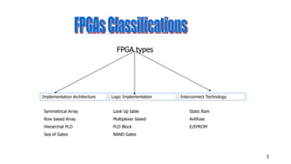
![9
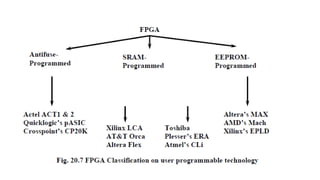
Company General
Architecture
Logic Block
Type
Programming
Technology
Xilinx Symmetrical Array Look-up Table Static RAM
Actel Row-based Multiplexer-Based Anti-fuse
Altera Hierarchical-PLD PLD Block EPROM
Plessey Sea-of-Gates NAND-gate Static RAM
PLUS Hierarchical-PLD PLD Block EPROM
AMD Hierarchical-PLD PLD Block EEPROM
QuickLogic Symmetrical Array Multiplexer-Based Anti-fuse
Algotronix Sea-of-gates Multiplexers & Basic
Gate
Static RAM
Concurrent Sea-of-gates Multiplexers & Basic
Gate
Static RAM
Crosspoint Row-based Transistors Pairs &
Multiplexers
Anti-fuse
FPGAs….[1]
Table 2.2 Summary of Commercially Available FPGAs](https://image.slidesharecdn.com/fpgaovervieworhangazi21-230616043432-77ae8a16/85/FPGA-9-320.jpg)


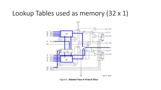
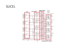
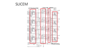
![Xilinx FPGAs - 50
Lookup Tables used as memory (16 x 2)
[ Distributed Memory ]](https://image.slidesharecdn.com/fpgaovervieworhangazi21-230616043432-77ae8a16/85/FPGA-50-320.jpg)