
Recommended
Recommended
More Related Content
Similar to Critical Factors for Reliable Chip Communication and ESD Protection
Similar to Critical Factors for Reliable Chip Communication and ESD Protection (20)
Recently uploaded
Recently uploaded (20)
Critical Factors for Reliable Chip Communication and ESD Protection
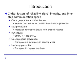
- 1. Introduction Critical factors of reliability, signal integrity, and inter- chip communication speed Clock generation and distribution • External clock source -> on-chip internal clock generation ESD protection • Protection for internal circuits from external hazards I/O circuits • CMOS <-> TTL or ECL On-chip noise prevention • From parasitic inductance in bonding wires Latch-up prevention • From parasitic bipolar transistors 1
- 2. ESD Protection 2 Human body model Charged device model, for ESD testing Machine model
- 3. Types of ESDs HBM(Human Body Model) Human body can induce 1.5kV • Condition – 80% relative humidity – Walking on synthetic carpet MM(Machine Model) Higher current than HBM CDM(Charged Device Model) Discharge of the packaged IC • Chip assembly or shipping -> Charge accumulation -> Discharge 3
- 4. Simplified Lumped-Element Model of HBM-ESD and MM-ESD Testers 4
- 5. ESD Protection Network Examples 5 Diffused resistor: 1-3kΩ Basic ESD protection network: diodes clamp the signal level -0.7V<VA<VDD+0.7V ID<several tens of mA Protection network with thick-oxide transistor: effective in excess of 3kV in HBM-ESD test M1, M2: thick oxide device w/ VT of 20~30V M3: thin oxide device operating in SAT region
- 6. ESD Failure 6 (a) Typical ESD failure modes (b) SEM photograph of a failed NMOS (from Diaz et al., 1994)
- 7. Input Series Transmission Gate 7 Schematic Symbol X=A when E=0 X=Z ,otherwise
- 8. Inverting Input Circuit with PN 8 Schematic Symbol • typical VIL=0.3VDD, VIH=0.7VDD for 30% noise margin
- 9. TTL to CMOS level shifting 9 Voltage level of TTL and CMOS The corresponding VTC 2.0V 0.8V
- 10. Designing the Receiving Inverter Gate(1) Adjust the TR ratio such that the saturation voltage at which both transistors operate in saturation region is the midpoint between 0.8V and 2.0V Saturation voltage of the inverter gate is 10 1 / / DD Tp Tn sat th n ox n n p ox p p V V rV V V r C W L r C W L
- 11. Designing the Receiving Inverter Gate(2) From these two equations, we get If and and , then in order to achieve The nMOS-to-pMOS ratio is 11 2 / / p DD Tp sat n n p p n sat Tn V V V W L W L V V p n 3 V V V Tp Tn 0 . 1 V VDD 5 V Vsat 4 . 1 2 0 . 2 8 . 0 12 169 1 4 . 1 4 . 1 1 5 3 1 / / 2 p p n n L W L W
- 12. Designing the Receiving Inverter Gate(3) From the above, we get that r=6.5 and where Vout satisfies the following: or 12 25 . 43 25 . 36 2 1 2 2 2 out Tp Tn DD out IL V r V V r V V V 2 2 2 2 1 2 out DD out DD Tp IL DD Tn IL V V V V V V V V V r 2 2 5 2 1 ) 5 )( 4 ( ) 1 ( 125 . 21 out out IL IL V V V V
- 13. Designing the Receiving Inverter Gate(4) Combining these two equations, and, hence Likewise, 13 V V V V V V out out out out out 97 . 4 5 2 1 ) 5 ( 25 . 43 2 75 . 136 25 . 43 7 2 125 . 21 2 2 V VIL 07 . 1 25 . 43 25 . 36 97 . 4 2 25 . 43 25 . 47 5 . 84 1 ) 2 ( 2 2 out Tp DD Tn out IH V r V V V V r V
- 14. Designing the Receiving Inverter Gate(5) where satisfies the following or Combining these two equations, we obtain Therefore, 14 out V 2 2 2 2 1 ) ( ) ( 2 1 out out Tn IH Tp IH DD V V V V r V V V 2 2 2 2 1 ) 1 ( 5 . 6 ) 4 ( 2 1 out out IH IH V V V V 2 2 2 1 25 . 43 4 5 . 84 25 . 42 25 . 43 25 . 47 5 . 84 4 2 1 out out out out V V V V V V V V IH out 47 . 1 206 . 0 and
- 15. Variation of the level-shifter VTC Variations to consider in simulation Process Temperature Supply voltage Process variation Strong pMOS(PH) - Weak nMOS(NL) Weak pMOS(PL) - Strong nMOS(NH) 15
- 16. Non-inverting TTL Level-shifting Circuit 16 Schematic Symbol
- 17. Input Pad Circuit with Schmitt Trigger 17 Schematic Symbol Negative-going logic threshold voltage=1V Positive-going logic threshold voltage=4V
- 18. Tristable Output Circuit 18 12 TRs Small area 4 TRs Large area (Last stage TRs need to be large) Symbol Circuit 1 Circuit 2
- 19. Typical Output Circuit Current During Switching (1) Capacitor load Initially charged to VDD=5V Sink the current to GND @ Clock signal Thus, 19 s max s max max DD load s max t I / t I dt di V C t I 2 2 2 2 4 s DD load max t V C dt di
- 20. Typical Output Circuit Current During Switching (2) If and , And for a bonding wire with L=2, 20 pF 100 load C ns 5 s t ns mA 80 2 9 12 max ) 10 5 ( 5 10 100 4 dt di mV 160 max dt di L
- 21. Circuit for Reducing (di/dt) Noise At strobe signal(ST), the last driver TRs are precharged If r=1 and ST=high, the gate voltages can be precharged to VDD/2 before CK goes to high 21
- 22. Another Circuit for Reducing (di/dt) Noise Transmits only differential signals 22
- 23. Timing Diagram Of the Driver Circuit The circuit produces pulses at nodes B and C only when input changes Output is at VDD/2 during the quiescent periods Phase splitter is used to generate differential pairs 23
- 24. Receiver Circuit for Differential Data 24
- 25. Bidirectional Buffer with TTL Input 25 (a) Schematic (b) Block diagram
- 26. Layout of a Bidirectional I/O Pad Circuit 26 Courtesy of MOSIS
- 27. On-Chip Clock Generation and Distribution Clock signal- heartbeats of digital systems Skew Spatial clock uncertainty due to PVT variations of clock buffers and interconnect lines in clock distribution network Jitter Temporal clock uncertainty from the clock generator and clock buffers About 10% of cycle time is expended to allow realistic clock jitter and skews in computer systems 27
- 28. Simple Clock Generator For low-end microprocessor chips Process-dependent Unstable 28
- 29. Pierce Crystal Oscillator Good frequency stability Near series-resonant circuit Internal series resistance and external load determines the frequency and stability Internal inverter generates the voltage difference External inverter amplify the clock signal 29
- 30. Phase-Locked Loop The most common on-chip clock generator Easy multiplication of frequency Frequency of VCO : N times as faster as the reference clock 30 PFD CP VCO Reference clock Divider /N UP DN LF Output clocks
- 31. D-FF D Q reset CLK D-FF CLK reset D Q Reference clock Divided VCO clock UP DN VDD VDD Phase Frequency Detector(PFD) 31
- 32. Output Pulses of PFD 32 Reference clock Divided VCO clock UP DN t Reference clock Divided VCO clock UP DN t Reference clock comes faster than the divided VCO clock UP The divided VCO clock comes earlier than the reference clock DN
- 33. Locked state of PLL Locked state of PLL Two clocks come very close Dead zone problem If the phase difference of two PFD inputs is as small as few pico seconds, the PFD cannot generate a proper pulse because it takes time for the PFD circuit to respond to the input signals In this case, the pulse width of PFD output would be too small to represent the exact amount of phase error It can be solved by inserting a buffer at the reset path to add some delay 33
- 34. Input and Output Characteristic of PFD 34 Vout -2π 2π ΔΦ
- 35. Oscillator Oscillator - unstable system that generates repetitive signals Oscillation conditions • Loop gain > 1 • Total phase shift = 360 Barkhausen criterion • Loop gain, phase shift: • Simple and intuitive • Bode plot • Necessary but not sufficient to stability Nyquist stability criterion • Accurate • Root-locus plot 35 0 0 1, 180 H j H j
- 36. Voltage Controlled Oscillator(VCO) VCO Oscillator whose frequency is controlled by the voltage Noise budget of the VCO • determines the jitter performance and loop bandwidth of PLL ωout : output frequency ω0 : initial VCO frequency KVCO : VCO gain VCTRL : VCO control voltage 36 dt V K CTRL VCO out 0
- 37. Factors to Consider in VCO (1) Free running frequency VCO operating frequency in the absence of control voltage Tuning range The range of frequency that VCO can generate It determines the operating range of PLL Noise rejection ability A measure of how much noise from external environment the VCO can filter out Supply noise rejection / Common-mode noise rejection 37
- 38. Factors to Consider in VCO (2) Power consumption Critical to low-power applications The more power, the better jitter performance Output signal purity The most important factor Clock jitter / phase noise 38
- 39. Harmonic Oscillator Resonance of the energy components such as LC- tank Good signal purity But bulky (inductor and capacitor) Tuning range – narrow Not suitable for digital systems 39 Capacitor Inductor BIAS OUT+ OUT-
- 40. Relaxation Oscillator Chain of delay elements Easy to design Compact size Bad signal purity Typical example: ring oscillator 40 VCTRL OUT
- 41. VCO with Supply Noise Rejection Regulated voltage ctrli robust to supply noise Opamp BW > PLL BW M1: large Enough voltage headroom Wide operating range of VCO M2: suppress ripples on ctrli Dominant pole on node ctrli Compensation capacitor and resistor are needed between node biasi and ctrli 41 M1 Vctrl biasi ctrli VDD VDD M2
- 42. Delay Cell Pseudo-differential type Back-to-back inverters are used ctrli controls the delay Body of PMOS is tied to the source Linear change in frequency 42 inp outp outn ctrli
- 43. Charge Pump(CP) 43 UP current source DN current source Icp IUP IDN S1 S2 Icp ΔΦ +Ia -Ia (a) Conceptual structure (b) Ideal output current of CP It has the phase error information
- 44. Loop Filter (1) Loop Filter(LF) converts current from CP to voltage One pole at VCO, the other pole at LF Two poles at DC -> Unstable 44 Icp Vctrl C - 40dB/dec log log 0 (DC) 0 (DC) Mag. Phase - 180° ctrl cp V 1 I sC
- 45. Loop Filter (2) Additional resistor introduces zero for larger phase margin 45 Icp Vctrl R C - 40dB/dec log log 0 (DC) 0 (DC) Mag. Phase - 180° - 90° Z ctrl cp V 1 1 I sRC R sC sC
- 46. Loop Filter (3) C2 reduces fluctuation caused by the IR drop 46 Icp Vctrl R C1 C2 Icp Vctrl R1 C1 C2 C3 C4 C5 Cn R3 R4 R5 Rn ctrl 1 2 cp 1 2 1 2 1 2 V 1 1 || I ( ) sRC R sC sC s RC C s C C Higher order LF Filters out noise Vctrl < Vcp =>Narrow range
- 47. All-Digital PLL(ADPLL) Issues in analog PLL in deep-submicron process 47 Leakage current in capacitors Steady-state power consumption Long-term jitter Small supply voltage High threshold voltage Narrow PLL operating range, high PLL noise sensitivity PFD DCO TDC DLF Divider CKin CKout ADPLL is introduced
- 48. Components of ADPLL Phase-Frequency Detector(PFD) Time-to-digital converter(TDC) converts phase difference to digital words replaces CP Digital loop filter(DLF) filters out digital input words Digitally controlled oscillator(DCO) replaces a VCO 48
- 49. Advantage/Disadvantage of ADPLL Advantage Excellent timing accuracy No analog circuits that suffer from small voltage headroom and relatively high threshold voltage Robust to PVT variation • Only TDC and DCO are sensitive Good for deep-submicron processes Disadvantage Limited resolution in phase detection by TDC Small resolution in frequency control by DCO Possibly more jitter than analog PLL 49
- 50. Delay-Locked Loop(DLL) VCDL adjusts the delay by a control voltage DLL adjusts the phase of VCDL / PLL modifies the frequency PLL has one more pole than DLL (2nd-order) No stability issue in DLL 50 PD CP UP Output clocks VCDL DN Reference clock LF
- 51. Simulation of DLL Locking Process Vctrl changes when abrupt phase shift occurs at 0ns and 500ns 51 Time (ns) Vctrl (V) 0 500 1000 0 -0.6 -1.2
- 52. Comparison of PLL and DLL PLL DLL VCO-Jitter accumulation VCDL–No jitter accumulation Higher-order system - Can be unstable - Hard to design 1st-order system - Always stable - Easier to design Costly to integrate LF Easier to integrate LF Less Ref. signal dependent Ref. signal dependent Easy Freq. multiplication Difficult Freq. multiplication No limited locking range Limited locking range TRef < VCDLdelay < 3TRef/2 EMI problem Less EMI Problem 52
- 53. Non-overlapping Clock Generator 53 Two phase clock generator Clock decoder symbol Clock decoder waveform Clock decoder schematic
- 54. Uniform Clock Distribution(H-tree) All clock signals are distributed with a uniform delay Difficult to achieve due to constraints of routing and fanout 54
- 55. Zero-Skew Network By CAD An example of the zero-skew clock routing network, generated by a computer-aided design(CAD) tool 55
- 56. Buffered Clock Distribution Network Every stage has the same number of fan- outs Essential for the balanced clock delays 56
- 57. Clock Distribution in the DEC Alpha Chip Mesh pattern of interconnect wires Clock signals are kept in phase across the entire chip 57
- 58. Considerations For VLSI Design Ideal duty cycle of a clock = 50% Feedback based on the voltage average improves the duty tr and tf should not be reduced excessively for prevention of reflection in the interconnection network Small load cap reduces the fan-out, the interconnect lengths, and the gate capacitances Small impedance of clock line by increasing the (w/h) ratios (the ratio of the line width to vertical separation distance of the line from the substrate) Cross-talk prevention Adequate separation between clock lines Power or ground rail between high-speed lines 58
- 59. Latch-Up (1) Silicon-controlled rectifier(SCR) with positive feedback Excessive current flow -> device damage Concerns of esp. I/O circuits 59 Cross-sectional view
- 60. Circuit Model of Latch-Up 60 Rwell: 1kΩ~20kΩ Rsub: a few Ω~several hundred Ω Assumption Rwell and Rsub are large enough to be neglected (open circuit) Initial condition Current gain: very low Only reverse leakage currents flows
- 61. Triggering the Latch-Up Trigger process IC of one of BJTs is increased by an external disturbance Feedback loop multiplies it by (β1· β2) -> positive feedback Low-impedance path is formed Trigger condition Or 61 1 1 1 1 2 1 2 2 1 1 α α α α α α 1 2 1 β β
- 62. Current-Voltage Characteristics of a SCR Voltage drop across the SCR in latch-up VH : holding voltage IH : holding current • Low impedance state if I>IH RT : total parasitic R in the current path 62 sat , CE sat , BE sat , CE sat , BE H V V V V V 1 2 2 1
- 63. Causes for Latch-Up Large slew rate of VDD during initial start-up Displacement currents • By well junction capacitance in the substrate and the well Dynamic recovery if the slew rate is not very high I/O signal swing much over VDD or far below VSS By impedance mismatches in transmission lines ESD stress Minority carrier injection: clamping device → substrate or well Sudden transients in buses Due to simultaneous switching of many drivers Leakage currents in well junctions Radiation of X-rays, cosmic rays, or alpha particles 63
- 64. From left figure, From relations of Q1 and Q2, : equivalent collector-to- emitter current gains absorbing the effects of parasitic R into TRs The SCR current I, Derivation of IH (1) 64 RS E RW E I I I I I I 2 1 I I I I I I E C E C 0 2 2 2 2 0 1 1 1 1 α α α α 0 2 0 1 α α , ) I I ( I I I CBO CBO C C 2 1 2 1
- 65. Derivation of IH (2) From above equations, IH is defined as the current with zero ICBO If α1+ α2 is close to 1, IH will be large The SCR current at the onset of latch-up, 65 ) α α ( ) α I α I ( I I RW RS CBO 2 1 2 1 1 1 2 1 2 1 α α α I α I I RW RS H T H DD H R / ) V V ( I I
- 66. Latch-Up Condition Both transistors are at the saturation boundary Therefore, the condition for latch-up is Above inequality shows that small Rsub and Rwell help avoiding the latch-up 66 sub RE RS well BE RW BE BE BE BE H R / V I R / V I V V V V V and with 2 1 2 2 1 2 1 2 1 BE DD sub T well T V V α R R α R R α α
- 67. Simulation of Latch-Up (Schematic) 67 (a) CMOS inverter with parasitic BJTs (b) Schematic of the simulation
- 68. Simulation of Latch-Up (Waveform) 68 (a) Voltage (b) Current
- 69. Latch-Up Guidelines(1) Gold doping of the substrate Reduce gains of BJTs by lowering the minority carrier lifetime Schottky source/drain contacts Reduce the minority carrier injection efficiency of BJT emitters Guardband rings: capture the injected minority carriers P+ guard rings connected to ground around nMOS N+ guard rings connected to VDD around pMOS Place substrate and well contacts as close as possible to the source of MOS transistors Reduce Rw and Rsub Minimum area p-wells (in case of twin-tub technology or n-type substrate) 69
- 70. Latch-Up Guidelines(2) Source diffusion regions of pMOS transistors should be placed. Ensure the same potential between VDD and p-wells In some n-well I/O circuits, wells can be eliminated by using only nMOS Avoid the forward biasing of source/drain junctions Prevents injecting high current Lightly doped epitaxial layer on top of a heavily doped substrate Shunts lateral currents from the vertical transistor Place nMOS close to VSS and pMOS near VDD Maintain sufficient space between pMOS and nMOS 70
- 71. I/O Cell Layout With Latch-Up Guidelines 71