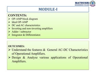
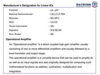
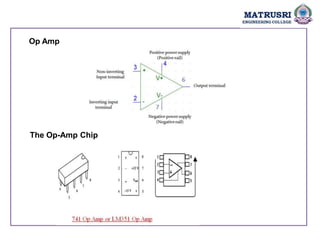
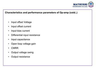
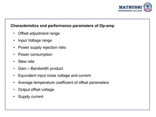
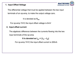
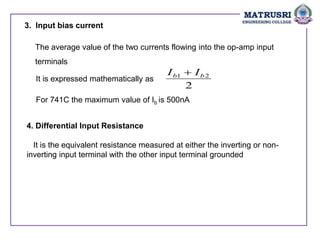
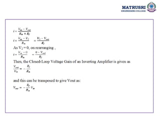
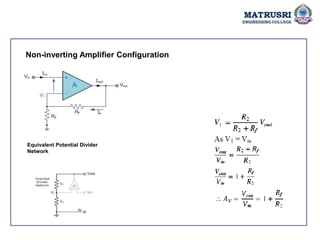
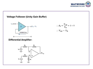
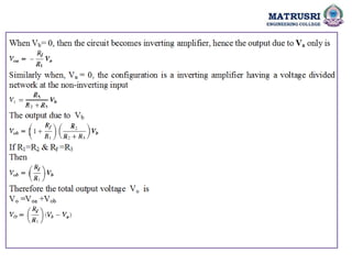
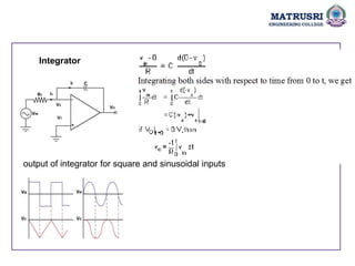
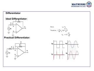
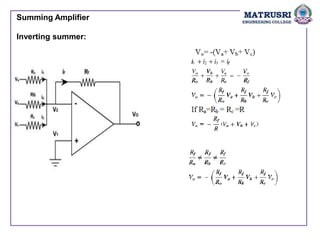
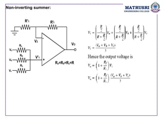
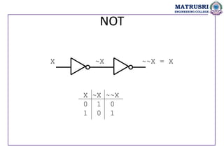
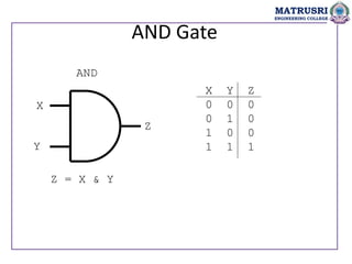
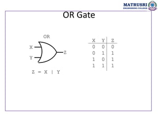
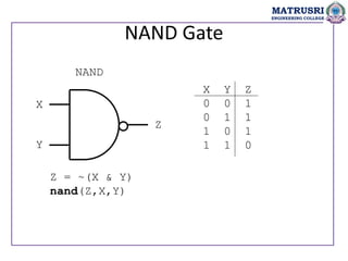
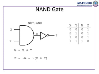
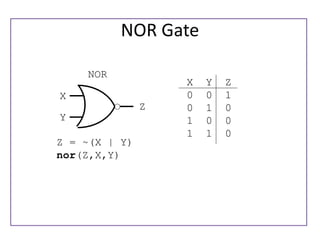
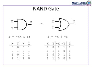
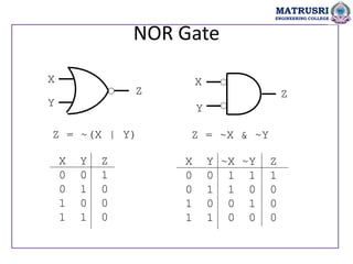
MATRUSRI ENGINEERING COLLEGE
DEPARTMENT OF INFORMATION TECHNOLOGY
SUBJECT NAME: BASIC ELECTRONICS
FACULTY NAME: K Praveen
MATRUSRI
ENGINEERING COLLEGE
BASIC ELECTRONICS
COURSE OBJECTIVES:
To understand the characteristics of diodes and transistor configurations.
2.To understand the design concepts of biasing of BJT and FET.
3.To understand the design concepts of feedback amplifiers and
oscillators.
4. To study the design concepts of OP Amp and data converters
characteristics of FETs, MOSFETs and study IC fabrication techniques.
MATRUSRI
ENGINEERING COLLEGE
BASIC ELECTRONICS
MATRUSRI
ENGINEERING COLLEGE
COURSE OUTCOMES:
On successful completion of this course, the students will be able to:
1.Study and analyse the rectifier and regulator circuits.
2.Study and analyse the performance of BJTs, FETs on the basis of their
operation and working.
3.Ability to analyse and design oscillator circuits.
4.Ability to analyse different logic gates and multivibrator circuits.
5.Ability to analyse different data acquisition systems.
UNIT-IV
MATRUSRI
ENGINEERING COLLEGE
Operational Amplifier: OP-AMP block diagram, Ideal OP-AMP , DC and
Ac characteristics, inverting and non-inverting amplifiers, adder /
subtractor , Integrator, Differentiator.
Logic Gate circuits: Introduction to digital systems-AND, NAND, NOR,
XOR gates, Binary half adder, full adder
OUTCOMES:
 Understand the features & General AC-DC Characteristics of
Operational Amplifiers.
 Design & Analyse various applications of Operational Amplifiers.
 Understand & Realise Digital systems-AND, NAND, NOR, XOR
gates, Binary half adder, full adder
MATRUSRI
ENGINEERING COLLEGE
OUTCOMES:
 Understand the features & General AC-DC Characteristics
of Operational Amplifiers.
 Design & Analyse various applications of Operational
Amplifiers.
MODULE-I
MATRUSRI
ENGINEERING COLLEGE
CONTENTS:
 OP-AMP block diagram
 Ideal OP-AMP
 DC and AC characteristics
 Inverting and non-inverting amplifiers
 Adder / subtractor
 Integrator & Differentiator.
Operational Amplifier:
• What is an Integrated Circuit?
• Where do you use an Integrated Circuit?
• Why do you prefer an Integrated Circuit to the circuits made by
interconnecting discrete components?
Def: The “Integrated Circuit “ or IC is a miniature, low
cost electronic circuit consisting of active and passive
components that are irreparably joined together on a
single crystal chip of silicon.
In 1958 Jack Kilby of Texas Instruments invented first IC
• Communication
• Control
• Instrumentation
• Computer
• Electronics
Applications of an Integrated Circuit
• Small size
• Low cost
• Less weight
• Low supply voltages
• Low power consumption
• Highly reliable
• Matched devices
• Fast speed
Advantages:
Classification
• Digital ICs
• Linear ICs
Pn junction
isolation
Hybrid circuits
Integrated circuits
Dielectric
isolation
Monolithic circuits
Bipolar Uni polar
MOSFET JFET
Classification of ICs
Thick
&Thin film
Chip size and Complexity
• Invention of Transistor (Ge)- 1947
• Development of Silicon- 1955-1959
• Silicon Planar Technology- 1959
• First ICs, SSI (3- 30gates/chip)- 1960
• MSI ( 30-300 gates/chip)- 1965-1970
• LSI ( 300-3000 gates/chip)-1970-1975
• VLSI (More than 3k gates/chip) - 1975
• ULSI (more than one million active devices are integrated on single
chip)
SSI MSI LSI VLSI ULSI
< 100 active
devices
100-1000
active
devices
1000-
100000
active
devices
>100000
active
devices
Over 1
million
active
devices
Integrated
resistors,
diodes &
BJT’s
BJT’s and
Enhanced
MOSFETS
MOSFETS 8bit, 16bit
Microproces
sors
Pentium
Microproces
sors
IC Package types
• Metal can Package
• Dual-in-line
• Flat Pack
Metal can Packages:
• The metal sealing plane is at the bottom over which the chip is bounded
• It is also called transistor pack
Dual-in-line Package
The chip is mounted inside a plastic or ceramic case
The 8 pin Dip is called MiniDIP and also available with 12, 14, 16, 20pins
Flat pack
The chip is enclosed in a rectangular ceramic case
Selection of IC Package
Type Criteria
Metal can
package
1. Heat dissipation is important
2. For high power applications like
power amplifiers, voltage regulators
etc.
DIP 1. For experimental or bread boarding
purposes as easy to mount
2. If bending or soldering of the leads is
not required
3. Suitable for printed circuit boards as
lead spacing is more
Flat pack 1. More reliability is required
2. Light in weight
3. Suited for airborne applications
Factors affecting selection of IC package
Temperature Ranges
1. Military temperature range : -55o C to +125o C (-55o C to +85o C)
2. Industrial temperature range : -20o C to +85o C (-40o C to +85o C )
3. Commercial temperature range: 0o C to +70o C (0o C to +75o C )
• Relative cost
• Reliability
• Weight of the package
• Ease of fabrication
• Power to be dissipated
• Need of external heat sink
Manufacturer’s Designation for Linear ICs
Fairchild - µA, µAF
National Semiconductor - LM,LH,LF,TBA
Motorola - MC,MFC
RCA - CA,CD
Texas Instruments - SN
Signetics - N/S,NE/SE
Burr- Brown - BB
Operational Amplifier
An “Operational amplifier” is a direct coupled high-gain amplifier usually
consisting of one or more differential amplifiers and usually followed by a
level translator and output stage.
The operational amplifier is a versatile device that can be used to amplify dc
as well as ac input signals and was originally designed for computing such
mathematical functions as addition, subtraction, multiplication and
integration.
Op Amp
The Op-Amp Chip
Single-Ended Input
Differential Amplifier
Characteristics and performance parameters of Op-amp (cotd..)
• Input offset Voltage
• Input offset current
• Input bias current
• Differential input resistance
• Input capacitance
• Open loop voltage gain
• CMRR
• Output voltage swing
• Output resistance
• Offset adjustment range
• Input Voltage range
• Power supply rejection ratio
• Power consumption
• Slew rate
• Gain – Bandwidth product
• Equivalent input noise voltage and current
• Average temperature coefficient of offset parameters
• Output offset voltage
• Supply current
Characteristics and performance parameters of Op-amp
1. Input Offset Voltage
The differential voltage that must be applied between the two input
terminals of an op-amp, to make the output voltage zero.
It is denoted as Vios
For op-amp 741C the input offset voltage is 6mV
2. Input offset current
The algebraic difference between the currents flowing into the two
input terminals of the op-amp
It is denoted as Iios = | Ib1 – Ib2|
For op-amp 741C the input offset current is 200nA
3. Input bias current
The average value of the two currents flowing into the op-amp input
terminals
It is expressed mathematically as
2
2
1 b
b I
I 
For 741C the maximum value of Ib is 500nA
4. Differential Input Resistance
It is the equivalent resistance measured at either the inverting or non-
inverting input terminal with the other input terminal grounded
5. Input capacitance
It is the equivalent capacitance measured at either the inverting or non-
inverting input terminal with the other input terminal grounded.
It is denoted as Ci
For 741C it is of the 1-4 pF
6. Open loop Voltage gain
It is the ratio of output voltage to the differential input voltage, when op-amp
is in open loop configuration, without any feedback. It is also called as large
signal voltage gain.
It is denoted as AOL AOL=Vo / Vd
For 741C it is typically 200,000
7. CMRR
It is the ratio of differential voltage gain Ad to common mode voltage gain Ac
CMRR = Ad / Ac
Ad is open loop voltage gain AOL and Ac = VOC / Vc
For op-amp 741C CMRR is 90 dB
8. Output Voltage swing
The op-amp output voltage gets saturated at +Vcc and –VEE and it cannot
produce output voltage more than +Vcc and –VEE. Practically voltages +Vsat
and –Vsat are slightly less than +Vcc and –VEE .
For op-amp 741C the saturation voltages are + 13V for supply voltages +
15V
9. Output Resistance
It is the equivalent resistance measured between the output terminal of the
op-amp and ground
It is denoted as Ro
For op-amp 741 it is 75Ω
10. Offset voltage adjustment range
The range for which input offset voltage can be adjusted using the
potentiometer so as to reduce output to zero
For op-amp 741C it is + 15mV
11. Input Voltage range
It is the range of common mode voltages which can be applied for which
op-amp functions properly and given offset specifications apply for the op-
amp
For + 15V supply voltages, the input voltage range is + 13V
12. Power supply rejection ratio
PSRR is defined as the ratio of the change in input offset voltage due to the
change in supply voltage producing it, keeping the other power supply voltage
constant. It is also called as power supply sensitivity (PSV)
PSRR= (Δvios / ΔVcc)|constant VEE
PSRR= (Δvios / ΔVEE)|constant Vcc
The typical value of PSRR for op-amp 741C is 30µV/V
13. Power Consumption
It is the amount of quiescent power to be consumed by op-amp with zero
input voltage, for its proper functioning
It is denoted as Pc
For 741C it is 85mW
14. Slew rate
Slew rate = S = dVo / dt |max
It is specified by the op-amp in unity gain condition. The slew rate is caused
due to limited charging rate of the compensation capacitor and current limiting
and saturation of the internal stages of op-amp, when a high frequency large
amplitude signal is applied.
It is given by dVc /dt = I/C
For large charging rate, the capacitor should be small or the current should be
large. S = Imax / C
For 741 IC the charging current is 15 µA and the internal capacitor is 30 pF.
S= 0.5V/ µsec
Slew rate equation
15. Gain – Bandwidth product
It is the bandwidth of op-amp when voltage gain is unity (1). It is denoted as
GB.
The GB is also called unity gain bandwidth (UGB) or closed loop bandwidth
It is about 1MHz for op-amp 741C
16. Equivalent Input Noise Voltage and Current
The noise is expressed as a power density
Thus equivalent noise voltage is expressed as V2 /Hz while the equivalent
noise current is expressed as A2 /Hz
17. Average temperature coefficient of offset parameters
The average rate of change of input offset voltage per unit change in
temperature is called average temperature coefficient of input offset
voltage or input offset voltage drift
It is measured in µV/oC. For 741 C it is 0.5 µV/oC
The average rate of change of input offset current per unit change in
temperature is called average temperature coefficient of input offset
current or input offset current drift
It is measured in nA/oC or pA/oC . For 741 C it is 12 pA/oC
18. Output offset voltage ( Voos )
The output offset voltage is the dc voltage present at the output
terminals when both the input terminals are grounded.
It is denoted as Voos
19. Supply current
It is drawn by the op-amp from the power supply
For op-amp 741C it is 2.8mA
Op amp equivalent circuit
Block diagram of op amp
The Ideal Operational Amplifier
• Open loop voltage gain AOL = ∞
• Input Impedance Ri = ∞
• Output Impedance Ro = 0
• Bandwidth BW = ∞
• Zero offset (Vo = 0 when V1 = V2 = 0) Vios = 0
• CMRR ρ = ∞
• Slew rate S = ∞
• No effect of temperature
• Power supply rejection ratio PSRR = 0
Ideal Op-amp
1.An ideal op-amp draws no current at both the input terminals I.e. I1 = I2 =
0. Thus its input impedance is infinite. Any source can drive it and there
is no loading on the driver stage
2.The gain of an ideal op-amp is infinite, hence the differential input Vd =
V1 – V2 is essentially zero for the finite output voltage Vo
3. The output voltage Vo is independent of the current drawn from the
output terminals. Thus its output impedance is zero and hence output can
drive an infinite number of other circuits
Op-amp Characteristics
DC Characteristics
• Input bias current
• Input offset current
• Input offset voltage
• Thermal drift
Ideal Voltage transfer curve
AC Characteristics
• Slew rate
• Frequency response
Practical voltage transfer curve
1. If Vd is greater than corresponding to b, the output attains +Vsat
2. If Vd is less than corresponding to a, the output attains –Vsat
3. Thus range a-b is input range for which output varies linearily
with the input. But AOL is very high, practically this range is very
small
Transient Response Rise time
When the output of the op-amp is suddenly changing like pulse type,
then the rise time of the response depends on the cut-off frequency fH
of the op-amp. Such a rise time is called cut-off frequency limited rise
time or transient response rise time ( tr )
H
r
f
t
35
.
0

Op-amp Characteristics
DC Characteristics
• Input bias current
• Input offset current
• Input offset voltage
• Thermal drift
AC Characteristics
• Slew rate
• Frequency response
Thermal Drift
The op-amp parameters input offset voltage Vios and input offset current Iios are
not constants but vary with the factors
1. Temperature
2. Supply Voltage changes
3. Time
Thermal Voltage Drift
It is defined as the average rate of change of input offset voltage per unit
change in temperature. It is also called as input offset voltage drift
Input offset voltage drift =
T
Vios


∆Vios = change in input offset voltage
∆T = Change in temperature
It is expressed in μV/0 c. The drift is not constant and it is not uniform over
specified operating temperature range
Input bias current drift
It is defined as the average rate of change of input bias current per unit
change in temperature
Thermal drift in input bias current =
T
Ib


It is measured in nA/oC or pA/oc. These parameters vary randomly
with temperature. i.e. they may be positive in one temperature range
and negative in another
Input Offset current drift
It is defined as the average rate of change of input offset current per unit
change in temperature
Thermal drift in input offset current =
T
Iios


AC Characteristics
Frequency Response
• Ideally, an op-amp should have an infinite bandwidth but practically
op-amp gain decreases at higher frequencies. Such a gain reduction
with respect to frequency is called as roll off.
• The plot showing the variations in magnitude and phase angle of the
gain due to the change in frequency is called frequency response of
the op-amp
The Differential Amplifier:
V1 = Vin1 and V2 = Vin2.
Vo = Ad (Vin1- Vin2 ) , where, Ad is
the open loop gain.
The Inverting Amplifier:
V1 = 0 and V2 = Vin
Vo = - Ad Vin
Open Loop mode:
The non-inverting amplifier
V1 = +Vin , V2 = 0 Vo = +Ad Vin
Closed Loop mode:
Inverting Amplifier Configuration
Non-inverting Amplifier Configuration
Equivalent Potential Divider
Network
Voltage Follower (Unity Gain Buffer)
Differential Amplifier:
Integrator
output of integrator for square and sinusoidal inputs
Differentiator
Ideal Differentiator:
Practical Differentiator:
Summing Amplifier
Inverting summer:
Non-inverting summer:
Subtractor:
Adder and Subtractor:
MATRUSRI
ENGINEERING COLLEGE
OUTCOMES:
 Understand & Realise Digital systems-AND, NAND, NOR, XOR
gates.
 Understand & Realise, Binary half adder & full adder
MODULE-II
MATRUSRI
ENGINEERING COLLEGE
CONTENTS:
 Introduction to digital systems
 AND, NAND, NOR, XOR gates
 Binary half adder
 full adder
NOT Gate -- Inverter
X Y
0
1
1
0
X Y
Y
NOT
X Y
Y = ~X
NOT
MATRUSRI
ENGINEERING COLLEGE
NOT
X ~X ~~X = X
X ~X ~~X
0 1 0
1 0 1
MATRUSRI
ENGINEERING COLLEGE
AND Gate
AND
X
Y
Z
Z = X & Y
X Y Z
0 0 0
0 1 0
1 0 0
1 1 1
MATRUSRI
ENGINEERING COLLEGE
OR Gate
OR
X
Y
Z
Z = X | Y
X Y Z
0 0 0
0 1 1
1 0 1
1 1 1
MATRUSRI
ENGINEERING COLLEGE
NAND Gate
NAND
X
Y
Z
X Y Z
0 0 1
0 1 1
1 0 1
1 1 0
Z = ~(X & Y)
nand(Z,X,Y)
MATRUSRI
ENGINEERING COLLEGE
NAND Gate
NOT-AND
X
Y
Z
W = X & Y
Z = ~W = ~(X & Y)
X Y W Z
0 0 0 1
0 1 0 1
1 0 0 1
1 1 1 0
W
MATRUSRI
ENGINEERING COLLEGE
NOR Gate
NOR
X
Y
Z
X Y Z
0 0 1
0 1 0
1 0 0
1 1 0
Z = ~(X | Y)
nor(Z,X,Y)
NOR Gate
NOT-OR
X
Y
W = X | Y
Z = ~W = ~(X | Y)
X Y W Z
0 0 0 1
0 1 1 0
1 0 1 0
1 1 1 0
Z
W
MATRUSRI
ENGINEERING COLLEGE
NAND Gate
X
Y
X
Y
Z Z
Z = ~(X & Y) Z = ~X | ~Y
=
X Y W Z
0 0 0 1
0 1 0 1
1 0 0 1
1 1 1 0
X Y ~X ~Y Z
0 0 1 1 1
0 1 1 0 1
1 0 0 1 1
1 1 0 0 0
MATRUSRI
ENGINEERING COLLEGE
NOR Gate
X
Y
Z
Z = ~(X | Y)
X Y Z
0 0 1
0 1 0
1 0 0
1 1 0
X
Y
Z
Z = ~X & ~Y
X Y ~X ~Y Z
0 0 1 1 1
0 1 1 0 0
1 0 0 1 0
1 1 0 0 0
MATRUSRI
ENGINEERING COLLEGE
Exclusive-OR Gate
X Y Z
XOR
X
Y
Z 0 0 0
0 1 1
1 0 1
1 1 0
Z = X ^ Y
xor(Z,X,Y)
MATRUSRI
ENGINEERING COLLEGE
Exclusive-NOR Gate
X Y Z
XNOR
X
Y
Z 0 0 1
0 1 0
1 0 0
1 1 1
Z = ~(X ^ Y)
Z = X ~^ Y
xnor(Z,X,Y)
MATRUSRI
ENGINEERING COLLEGE
MATRUSRI
ENGINEERING COLLEGE
MATRUSRI
ENGINEERING COLLEGE
MATRUSRI
ENGINEERING COLLEGE
MATRUSRI
ENGINEERING COLLEGE
MATRUSRI
ENGINEERING COLLEGE
Short Answer Questions
1. Why NAND and NOR gates are called universal gates?
2. List the ideal characteristics of an OP-AMP?
3. Realize the basic logic gates using NAND gates?
4. Distinguish between combinational and sequential circuits.
5. What is an op-amp? List the building blocks of op-amp.
6. Define the terms slew rate and CMRR.
7. How a half adder can be converted into full adder?
8. What is the importance of logic gates? Draw the truth
tables for basic gates?
9. What is an instrumentation amplifier?
10. Distinguish between differentiator and integrator.
MATRUSRI
ENGINEERING COLLEGE
Long Answer Questions
1. Draw the op-amp as non-inverting amplifier and derive the
equation for its gain?
2. Draw the OP-AMP summing amplifier circuit and obtain an
expression for the output voltage for four inputs.
3. Realize half adder and full adder using NAND gates.
4. Draw the functional block diagram of an op-amp and
explain function of each block.
5. How the OP-AMP acts as integrator and differentiator &
derive its required equations?

Basic Electronic UNIT-IV PPT

  • 1.
    MATRUSRI ENGINEERING COLLEGE DEPARTMENTOF INFORMATION TECHNOLOGY SUBJECT NAME: BASIC ELECTRONICS FACULTY NAME: K Praveen MATRUSRI ENGINEERING COLLEGE
  • 2.
    BASIC ELECTRONICS COURSE OBJECTIVES: Tounderstand the characteristics of diodes and transistor configurations. 2.To understand the design concepts of biasing of BJT and FET. 3.To understand the design concepts of feedback amplifiers and oscillators. 4. To study the design concepts of OP Amp and data converters characteristics of FETs, MOSFETs and study IC fabrication techniques. MATRUSRI ENGINEERING COLLEGE
  • 3.
    BASIC ELECTRONICS MATRUSRI ENGINEERING COLLEGE COURSEOUTCOMES: On successful completion of this course, the students will be able to: 1.Study and analyse the rectifier and regulator circuits. 2.Study and analyse the performance of BJTs, FETs on the basis of their operation and working. 3.Ability to analyse and design oscillator circuits. 4.Ability to analyse different logic gates and multivibrator circuits. 5.Ability to analyse different data acquisition systems.
  • 4.
    UNIT-IV MATRUSRI ENGINEERING COLLEGE Operational Amplifier:OP-AMP block diagram, Ideal OP-AMP , DC and Ac characteristics, inverting and non-inverting amplifiers, adder / subtractor , Integrator, Differentiator. Logic Gate circuits: Introduction to digital systems-AND, NAND, NOR, XOR gates, Binary half adder, full adder OUTCOMES:  Understand the features & General AC-DC Characteristics of Operational Amplifiers.  Design & Analyse various applications of Operational Amplifiers.  Understand & Realise Digital systems-AND, NAND, NOR, XOR gates, Binary half adder, full adder
  • 5.
    MATRUSRI ENGINEERING COLLEGE OUTCOMES:  Understandthe features & General AC-DC Characteristics of Operational Amplifiers.  Design & Analyse various applications of Operational Amplifiers. MODULE-I MATRUSRI ENGINEERING COLLEGE CONTENTS:  OP-AMP block diagram  Ideal OP-AMP  DC and AC characteristics  Inverting and non-inverting amplifiers  Adder / subtractor  Integrator & Differentiator.
  • 6.
    Operational Amplifier: • Whatis an Integrated Circuit? • Where do you use an Integrated Circuit? • Why do you prefer an Integrated Circuit to the circuits made by interconnecting discrete components?
  • 7.
    Def: The “IntegratedCircuit “ or IC is a miniature, low cost electronic circuit consisting of active and passive components that are irreparably joined together on a single crystal chip of silicon. In 1958 Jack Kilby of Texas Instruments invented first IC
  • 8.
    • Communication • Control •Instrumentation • Computer • Electronics Applications of an Integrated Circuit
  • 9.
    • Small size •Low cost • Less weight • Low supply voltages • Low power consumption • Highly reliable • Matched devices • Fast speed Advantages:
  • 10.
    Classification • Digital ICs •Linear ICs Pn junction isolation Hybrid circuits Integrated circuits Dielectric isolation Monolithic circuits Bipolar Uni polar MOSFET JFET Classification of ICs Thick &Thin film
  • 11.
    Chip size andComplexity • Invention of Transistor (Ge)- 1947 • Development of Silicon- 1955-1959 • Silicon Planar Technology- 1959 • First ICs, SSI (3- 30gates/chip)- 1960 • MSI ( 30-300 gates/chip)- 1965-1970 • LSI ( 300-3000 gates/chip)-1970-1975 • VLSI (More than 3k gates/chip) - 1975 • ULSI (more than one million active devices are integrated on single chip)
  • 12.
    SSI MSI LSIVLSI ULSI < 100 active devices 100-1000 active devices 1000- 100000 active devices >100000 active devices Over 1 million active devices Integrated resistors, diodes & BJT’s BJT’s and Enhanced MOSFETS MOSFETS 8bit, 16bit Microproces sors Pentium Microproces sors
  • 13.
    IC Package types •Metal can Package • Dual-in-line • Flat Pack Metal can Packages: • The metal sealing plane is at the bottom over which the chip is bounded • It is also called transistor pack
  • 14.
    Dual-in-line Package The chipis mounted inside a plastic or ceramic case The 8 pin Dip is called MiniDIP and also available with 12, 14, 16, 20pins Flat pack The chip is enclosed in a rectangular ceramic case
  • 15.
    Selection of ICPackage Type Criteria Metal can package 1. Heat dissipation is important 2. For high power applications like power amplifiers, voltage regulators etc. DIP 1. For experimental or bread boarding purposes as easy to mount 2. If bending or soldering of the leads is not required 3. Suitable for printed circuit boards as lead spacing is more Flat pack 1. More reliability is required 2. Light in weight 3. Suited for airborne applications
  • 16.
    Factors affecting selectionof IC package Temperature Ranges 1. Military temperature range : -55o C to +125o C (-55o C to +85o C) 2. Industrial temperature range : -20o C to +85o C (-40o C to +85o C ) 3. Commercial temperature range: 0o C to +70o C (0o C to +75o C ) • Relative cost • Reliability • Weight of the package • Ease of fabrication • Power to be dissipated • Need of external heat sink
  • 17.
    Manufacturer’s Designation forLinear ICs Fairchild - µA, µAF National Semiconductor - LM,LH,LF,TBA Motorola - MC,MFC RCA - CA,CD Texas Instruments - SN Signetics - N/S,NE/SE Burr- Brown - BB Operational Amplifier An “Operational amplifier” is a direct coupled high-gain amplifier usually consisting of one or more differential amplifiers and usually followed by a level translator and output stage. The operational amplifier is a versatile device that can be used to amplify dc as well as ac input signals and was originally designed for computing such mathematical functions as addition, subtraction, multiplication and integration.
  • 18.
  • 19.
  • 20.
  • 21.
    Characteristics and performanceparameters of Op-amp (cotd..) • Input offset Voltage • Input offset current • Input bias current • Differential input resistance • Input capacitance • Open loop voltage gain • CMRR • Output voltage swing • Output resistance
  • 22.
    • Offset adjustmentrange • Input Voltage range • Power supply rejection ratio • Power consumption • Slew rate • Gain – Bandwidth product • Equivalent input noise voltage and current • Average temperature coefficient of offset parameters • Output offset voltage • Supply current Characteristics and performance parameters of Op-amp
  • 23.
    1. Input OffsetVoltage The differential voltage that must be applied between the two input terminals of an op-amp, to make the output voltage zero. It is denoted as Vios For op-amp 741C the input offset voltage is 6mV 2. Input offset current The algebraic difference between the currents flowing into the two input terminals of the op-amp It is denoted as Iios = | Ib1 – Ib2| For op-amp 741C the input offset current is 200nA
  • 24.
    3. Input biascurrent The average value of the two currents flowing into the op-amp input terminals It is expressed mathematically as 2 2 1 b b I I  For 741C the maximum value of Ib is 500nA 4. Differential Input Resistance It is the equivalent resistance measured at either the inverting or non- inverting input terminal with the other input terminal grounded
  • 25.
    5. Input capacitance Itis the equivalent capacitance measured at either the inverting or non- inverting input terminal with the other input terminal grounded. It is denoted as Ci For 741C it is of the 1-4 pF 6. Open loop Voltage gain It is the ratio of output voltage to the differential input voltage, when op-amp is in open loop configuration, without any feedback. It is also called as large signal voltage gain. It is denoted as AOL AOL=Vo / Vd For 741C it is typically 200,000
  • 26.
    7. CMRR It isthe ratio of differential voltage gain Ad to common mode voltage gain Ac CMRR = Ad / Ac Ad is open loop voltage gain AOL and Ac = VOC / Vc For op-amp 741C CMRR is 90 dB 8. Output Voltage swing The op-amp output voltage gets saturated at +Vcc and –VEE and it cannot produce output voltage more than +Vcc and –VEE. Practically voltages +Vsat and –Vsat are slightly less than +Vcc and –VEE . For op-amp 741C the saturation voltages are + 13V for supply voltages + 15V
  • 27.
    9. Output Resistance Itis the equivalent resistance measured between the output terminal of the op-amp and ground It is denoted as Ro For op-amp 741 it is 75Ω 10. Offset voltage adjustment range The range for which input offset voltage can be adjusted using the potentiometer so as to reduce output to zero For op-amp 741C it is + 15mV
  • 28.
    11. Input Voltagerange It is the range of common mode voltages which can be applied for which op-amp functions properly and given offset specifications apply for the op- amp For + 15V supply voltages, the input voltage range is + 13V 12. Power supply rejection ratio PSRR is defined as the ratio of the change in input offset voltage due to the change in supply voltage producing it, keeping the other power supply voltage constant. It is also called as power supply sensitivity (PSV) PSRR= (Δvios / ΔVcc)|constant VEE PSRR= (Δvios / ΔVEE)|constant Vcc The typical value of PSRR for op-amp 741C is 30µV/V
  • 29.
    13. Power Consumption Itis the amount of quiescent power to be consumed by op-amp with zero input voltage, for its proper functioning It is denoted as Pc For 741C it is 85mW 14. Slew rate Slew rate = S = dVo / dt |max It is specified by the op-amp in unity gain condition. The slew rate is caused due to limited charging rate of the compensation capacitor and current limiting and saturation of the internal stages of op-amp, when a high frequency large amplitude signal is applied. It is given by dVc /dt = I/C For large charging rate, the capacitor should be small or the current should be large. S = Imax / C For 741 IC the charging current is 15 µA and the internal capacitor is 30 pF. S= 0.5V/ µsec
  • 30.
  • 31.
    15. Gain –Bandwidth product It is the bandwidth of op-amp when voltage gain is unity (1). It is denoted as GB. The GB is also called unity gain bandwidth (UGB) or closed loop bandwidth It is about 1MHz for op-amp 741C 16. Equivalent Input Noise Voltage and Current The noise is expressed as a power density Thus equivalent noise voltage is expressed as V2 /Hz while the equivalent noise current is expressed as A2 /Hz
  • 32.
    17. Average temperaturecoefficient of offset parameters The average rate of change of input offset voltage per unit change in temperature is called average temperature coefficient of input offset voltage or input offset voltage drift It is measured in µV/oC. For 741 C it is 0.5 µV/oC The average rate of change of input offset current per unit change in temperature is called average temperature coefficient of input offset current or input offset current drift It is measured in nA/oC or pA/oC . For 741 C it is 12 pA/oC
  • 33.
    18. Output offsetvoltage ( Voos ) The output offset voltage is the dc voltage present at the output terminals when both the input terminals are grounded. It is denoted as Voos 19. Supply current It is drawn by the op-amp from the power supply For op-amp 741C it is 2.8mA Op amp equivalent circuit
  • 34.
  • 35.
    The Ideal OperationalAmplifier • Open loop voltage gain AOL = ∞ • Input Impedance Ri = ∞ • Output Impedance Ro = 0 • Bandwidth BW = ∞ • Zero offset (Vo = 0 when V1 = V2 = 0) Vios = 0 • CMRR ρ = ∞ • Slew rate S = ∞ • No effect of temperature • Power supply rejection ratio PSRR = 0
  • 36.
    Ideal Op-amp 1.An idealop-amp draws no current at both the input terminals I.e. I1 = I2 = 0. Thus its input impedance is infinite. Any source can drive it and there is no loading on the driver stage 2.The gain of an ideal op-amp is infinite, hence the differential input Vd = V1 – V2 is essentially zero for the finite output voltage Vo 3. The output voltage Vo is independent of the current drawn from the output terminals. Thus its output impedance is zero and hence output can drive an infinite number of other circuits
  • 37.
    Op-amp Characteristics DC Characteristics •Input bias current • Input offset current • Input offset voltage • Thermal drift Ideal Voltage transfer curve AC Characteristics • Slew rate • Frequency response
  • 38.
    Practical voltage transfercurve 1. If Vd is greater than corresponding to b, the output attains +Vsat 2. If Vd is less than corresponding to a, the output attains –Vsat 3. Thus range a-b is input range for which output varies linearily with the input. But AOL is very high, practically this range is very small Transient Response Rise time When the output of the op-amp is suddenly changing like pulse type, then the rise time of the response depends on the cut-off frequency fH of the op-amp. Such a rise time is called cut-off frequency limited rise time or transient response rise time ( tr ) H r f t 35 . 0 
  • 39.
    Op-amp Characteristics DC Characteristics •Input bias current • Input offset current • Input offset voltage • Thermal drift AC Characteristics • Slew rate • Frequency response
  • 40.
    Thermal Drift The op-ampparameters input offset voltage Vios and input offset current Iios are not constants but vary with the factors 1. Temperature 2. Supply Voltage changes 3. Time Thermal Voltage Drift It is defined as the average rate of change of input offset voltage per unit change in temperature. It is also called as input offset voltage drift Input offset voltage drift = T Vios   ∆Vios = change in input offset voltage ∆T = Change in temperature It is expressed in μV/0 c. The drift is not constant and it is not uniform over specified operating temperature range
  • 41.
    Input bias currentdrift It is defined as the average rate of change of input bias current per unit change in temperature Thermal drift in input bias current = T Ib   It is measured in nA/oC or pA/oc. These parameters vary randomly with temperature. i.e. they may be positive in one temperature range and negative in another Input Offset current drift It is defined as the average rate of change of input offset current per unit change in temperature Thermal drift in input offset current = T Iios  
  • 42.
    AC Characteristics Frequency Response •Ideally, an op-amp should have an infinite bandwidth but practically op-amp gain decreases at higher frequencies. Such a gain reduction with respect to frequency is called as roll off. • The plot showing the variations in magnitude and phase angle of the gain due to the change in frequency is called frequency response of the op-amp
  • 43.
    The Differential Amplifier: V1= Vin1 and V2 = Vin2. Vo = Ad (Vin1- Vin2 ) , where, Ad is the open loop gain. The Inverting Amplifier: V1 = 0 and V2 = Vin Vo = - Ad Vin Open Loop mode:
  • 44.
    The non-inverting amplifier V1= +Vin , V2 = 0 Vo = +Ad Vin Closed Loop mode: Inverting Amplifier Configuration
  • 46.
  • 47.
    Voltage Follower (UnityGain Buffer) Differential Amplifier:
  • 49.
    Integrator output of integratorfor square and sinusoidal inputs
  • 50.
  • 51.
  • 52.
  • 53.
  • 54.
  • 55.
    MATRUSRI ENGINEERING COLLEGE OUTCOMES:  Understand& Realise Digital systems-AND, NAND, NOR, XOR gates.  Understand & Realise, Binary half adder & full adder MODULE-II MATRUSRI ENGINEERING COLLEGE CONTENTS:  Introduction to digital systems  AND, NAND, NOR, XOR gates  Binary half adder  full adder
  • 56.
    NOT Gate --Inverter X Y 0 1 1 0 X Y Y NOT X Y Y = ~X NOT MATRUSRI ENGINEERING COLLEGE
  • 57.
    NOT X ~X ~~X= X X ~X ~~X 0 1 0 1 0 1 MATRUSRI ENGINEERING COLLEGE
  • 58.
    AND Gate AND X Y Z Z =X & Y X Y Z 0 0 0 0 1 0 1 0 0 1 1 1 MATRUSRI ENGINEERING COLLEGE
  • 59.
    OR Gate OR X Y Z Z =X | Y X Y Z 0 0 0 0 1 1 1 0 1 1 1 1 MATRUSRI ENGINEERING COLLEGE
  • 60.
    NAND Gate NAND X Y Z X YZ 0 0 1 0 1 1 1 0 1 1 1 0 Z = ~(X & Y) nand(Z,X,Y) MATRUSRI ENGINEERING COLLEGE
  • 61.
    NAND Gate NOT-AND X Y Z W =X & Y Z = ~W = ~(X & Y) X Y W Z 0 0 0 1 0 1 0 1 1 0 0 1 1 1 1 0 W MATRUSRI ENGINEERING COLLEGE
  • 62.
    NOR Gate NOR X Y Z X YZ 0 0 1 0 1 0 1 0 0 1 1 0 Z = ~(X | Y) nor(Z,X,Y)
  • 63.
    NOR Gate NOT-OR X Y W =X | Y Z = ~W = ~(X | Y) X Y W Z 0 0 0 1 0 1 1 0 1 0 1 0 1 1 1 0 Z W MATRUSRI ENGINEERING COLLEGE
  • 64.
    NAND Gate X Y X Y Z Z Z= ~(X & Y) Z = ~X | ~Y = X Y W Z 0 0 0 1 0 1 0 1 1 0 0 1 1 1 1 0 X Y ~X ~Y Z 0 0 1 1 1 0 1 1 0 1 1 0 0 1 1 1 1 0 0 0 MATRUSRI ENGINEERING COLLEGE
  • 65.
    NOR Gate X Y Z Z =~(X | Y) X Y Z 0 0 1 0 1 0 1 0 0 1 1 0 X Y Z Z = ~X & ~Y X Y ~X ~Y Z 0 0 1 1 1 0 1 1 0 0 1 0 0 1 0 1 1 0 0 0 MATRUSRI ENGINEERING COLLEGE
  • 66.
    Exclusive-OR Gate X YZ XOR X Y Z 0 0 0 0 1 1 1 0 1 1 1 0 Z = X ^ Y xor(Z,X,Y) MATRUSRI ENGINEERING COLLEGE
  • 67.
    Exclusive-NOR Gate X YZ XNOR X Y Z 0 0 1 0 1 0 1 0 0 1 1 1 Z = ~(X ^ Y) Z = X ~^ Y xnor(Z,X,Y) MATRUSRI ENGINEERING COLLEGE
  • 68.
  • 69.
  • 70.
  • 71.
  • 72.
    MATRUSRI ENGINEERING COLLEGE Short AnswerQuestions 1. Why NAND and NOR gates are called universal gates? 2. List the ideal characteristics of an OP-AMP? 3. Realize the basic logic gates using NAND gates? 4. Distinguish between combinational and sequential circuits. 5. What is an op-amp? List the building blocks of op-amp. 6. Define the terms slew rate and CMRR. 7. How a half adder can be converted into full adder? 8. What is the importance of logic gates? Draw the truth tables for basic gates? 9. What is an instrumentation amplifier? 10. Distinguish between differentiator and integrator.
  • 73.
    MATRUSRI ENGINEERING COLLEGE Long AnswerQuestions 1. Draw the op-amp as non-inverting amplifier and derive the equation for its gain? 2. Draw the OP-AMP summing amplifier circuit and obtain an expression for the output voltage for four inputs. 3. Realize half adder and full adder using NAND gates. 4. Draw the functional block diagram of an op-amp and explain function of each block. 5. How the OP-AMP acts as integrator and differentiator & derive its required equations?