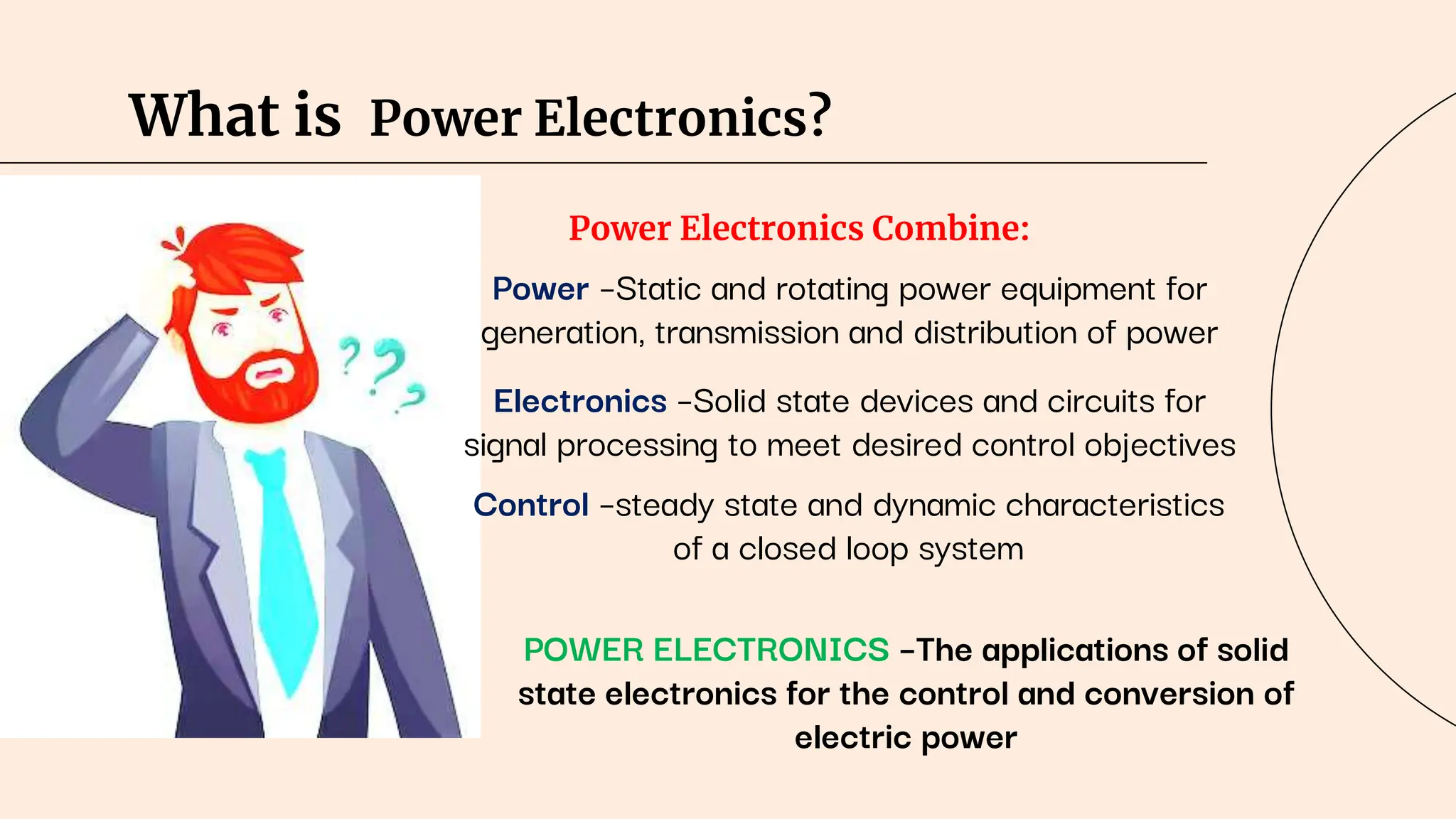
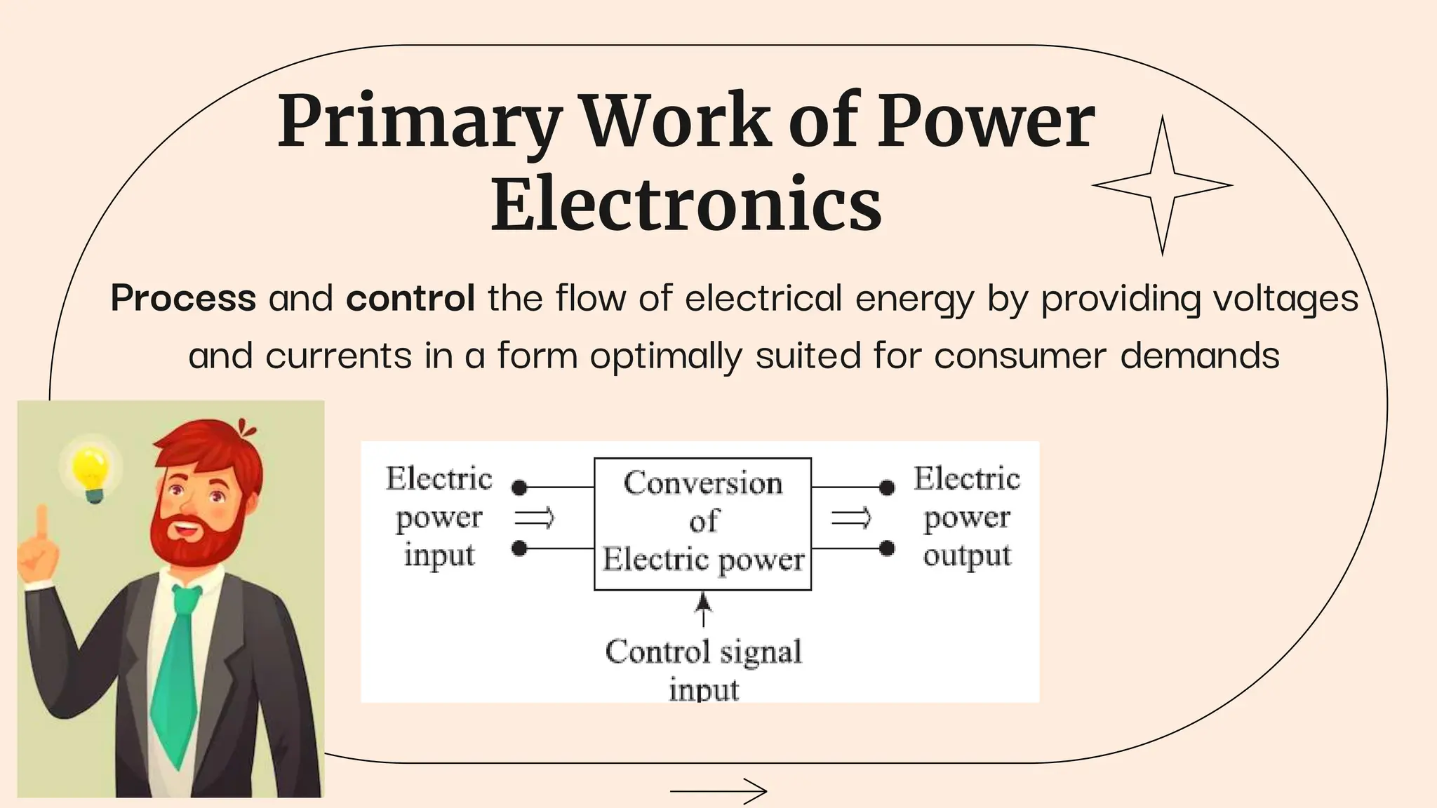
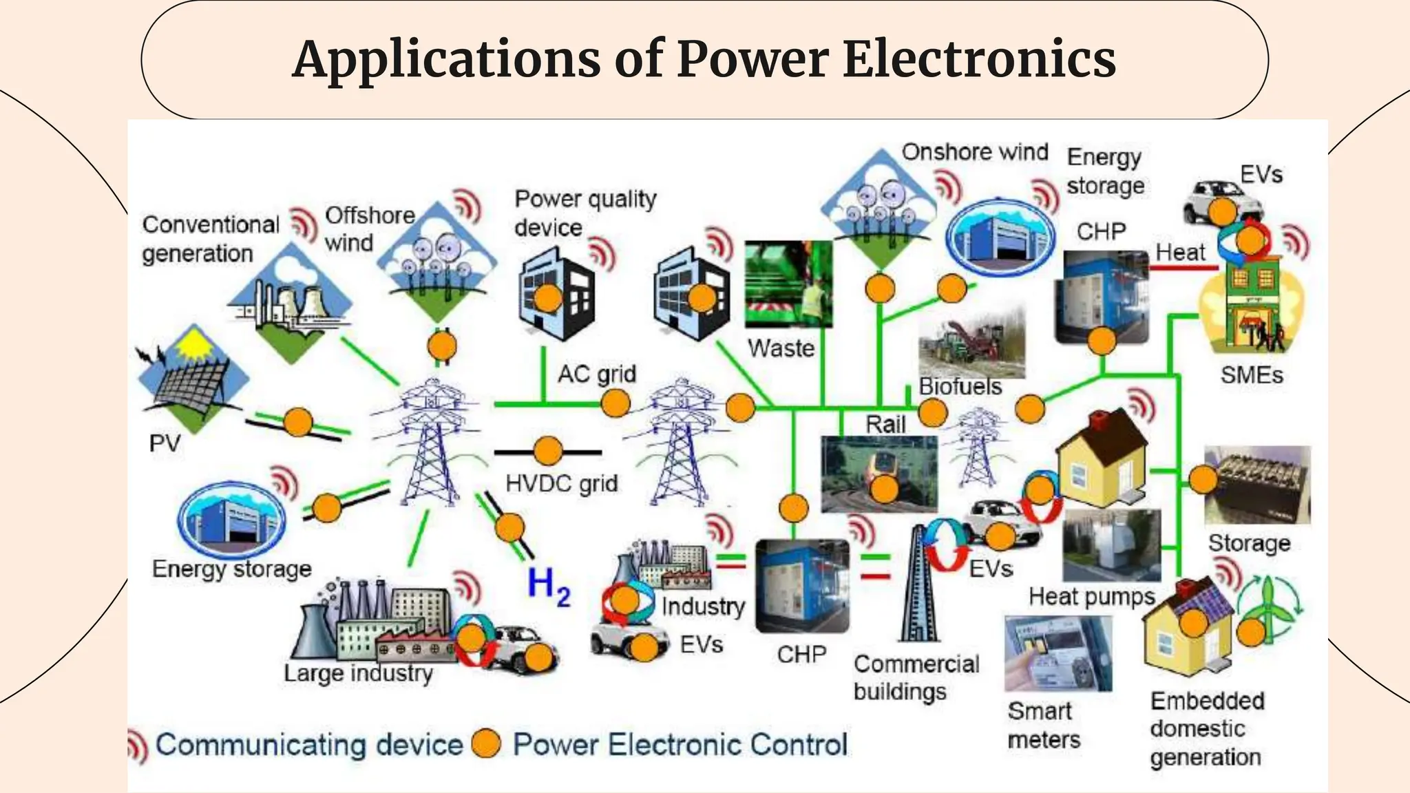
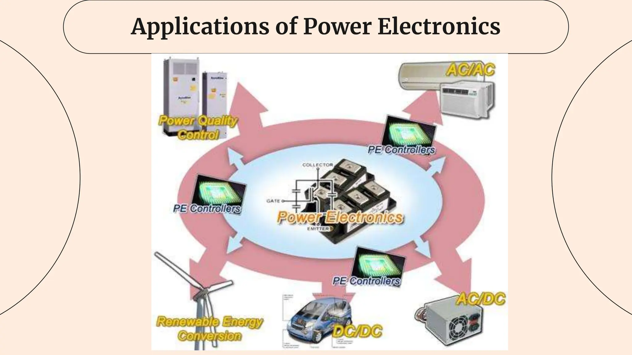
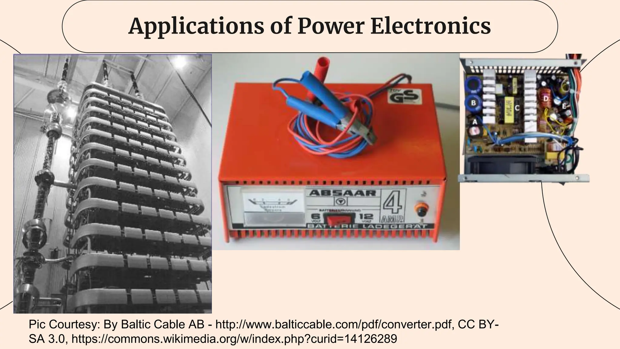
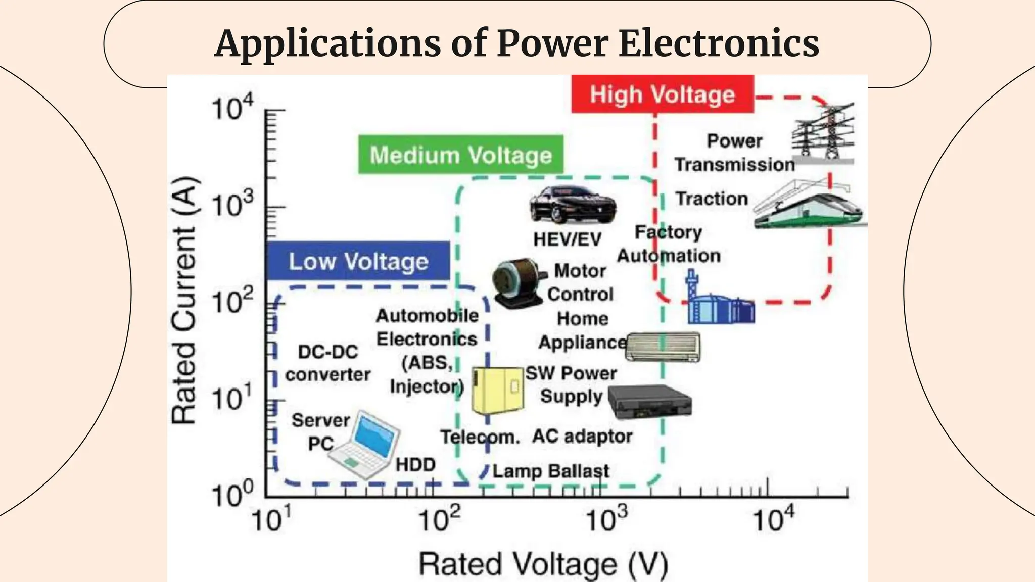
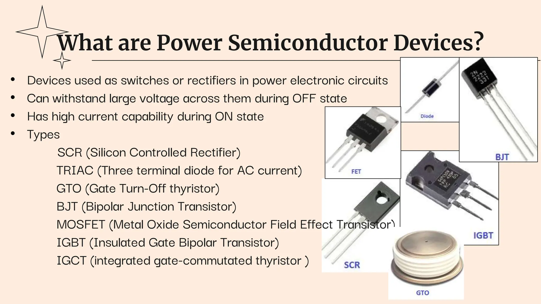
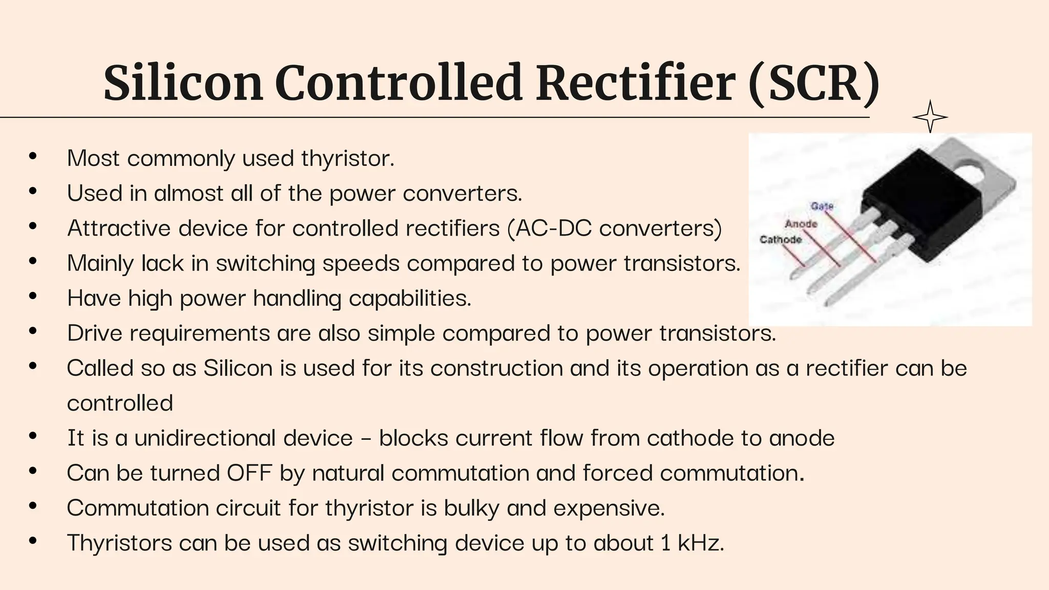
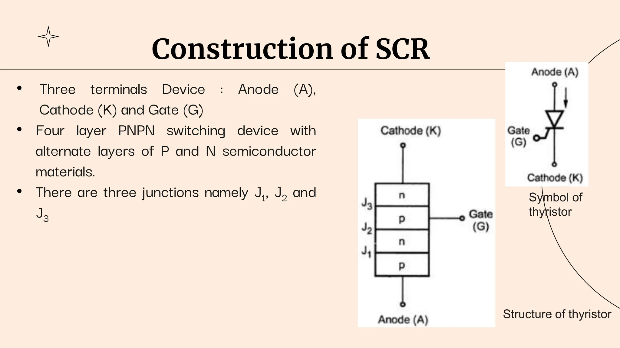
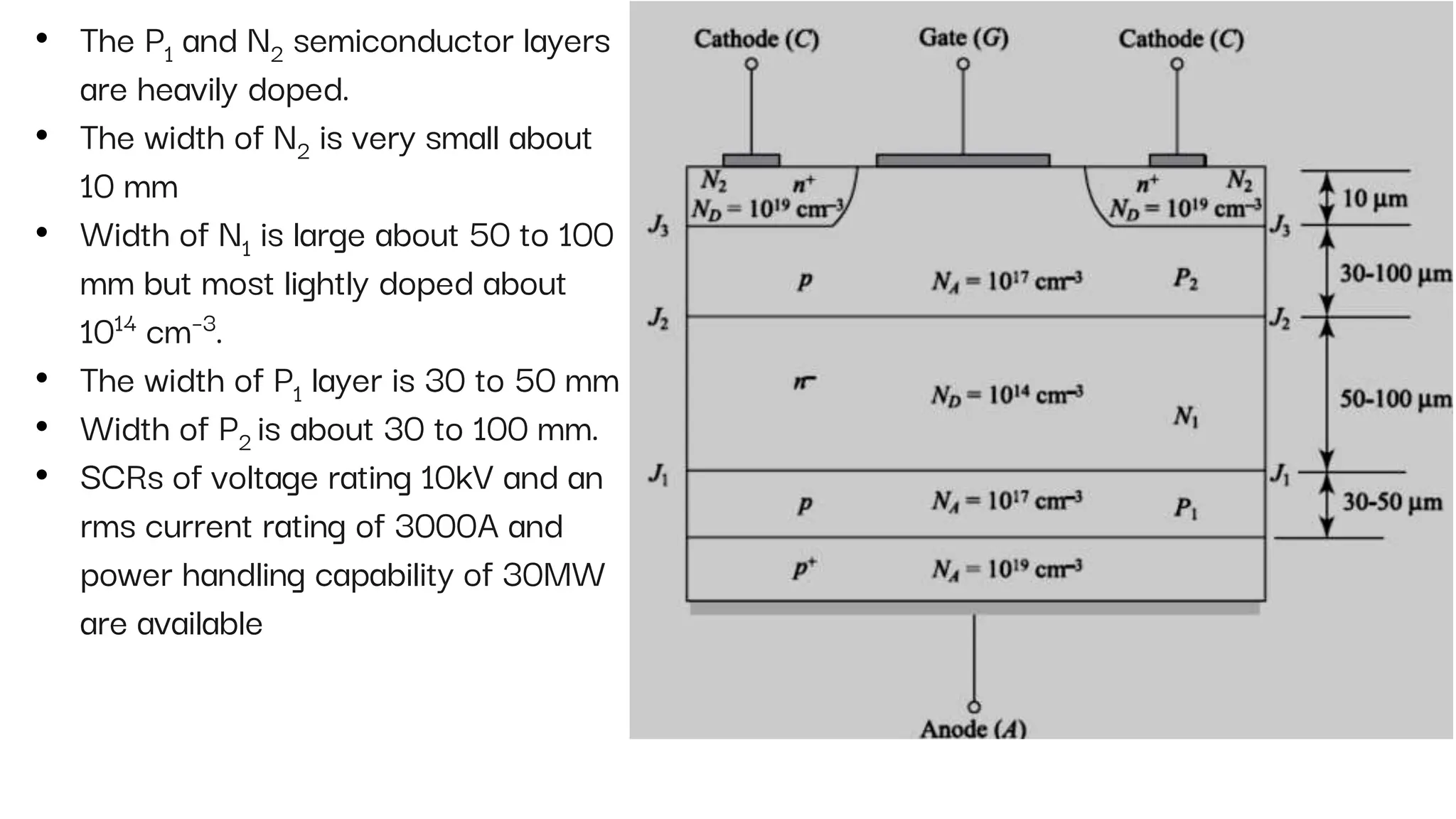
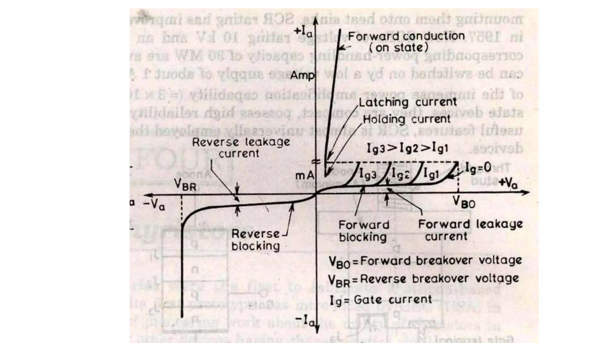
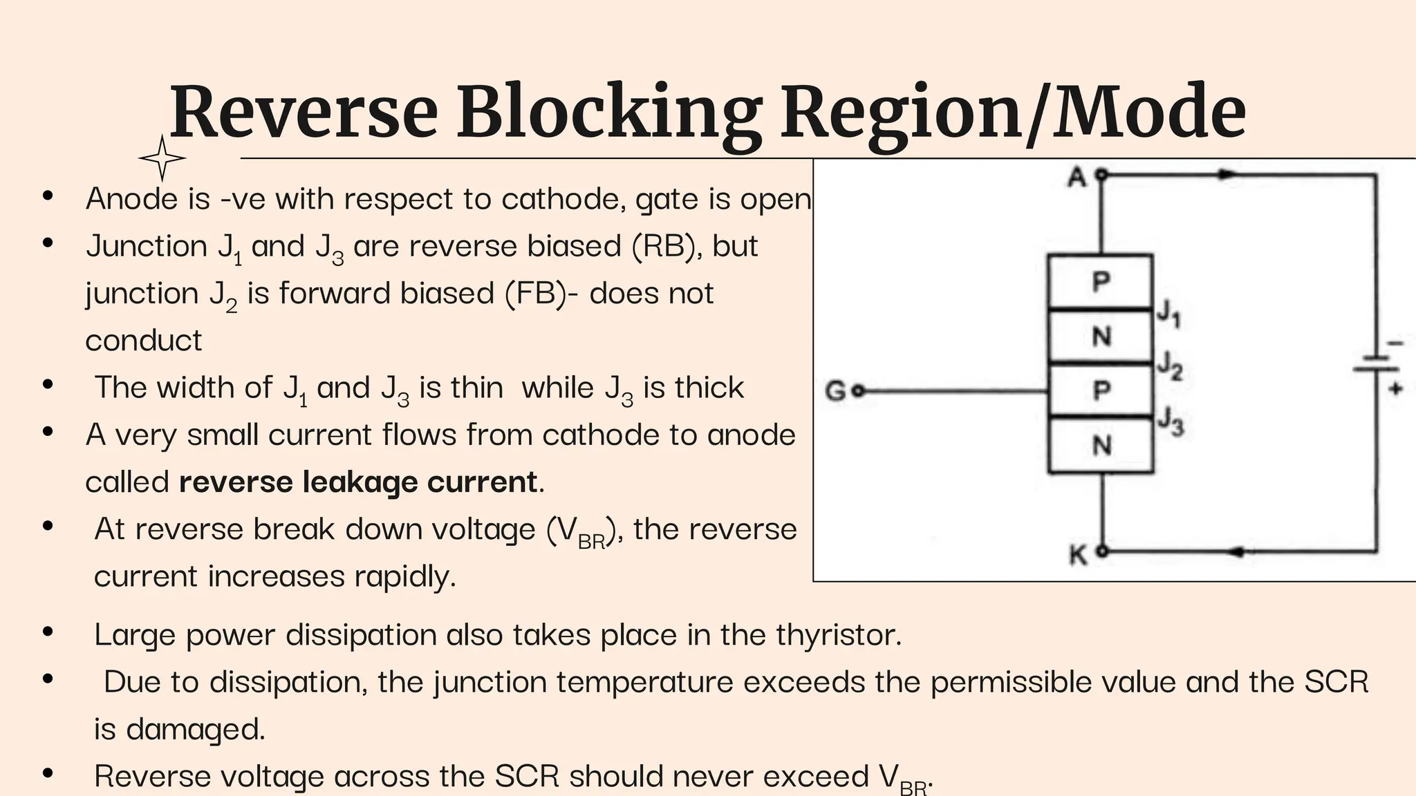
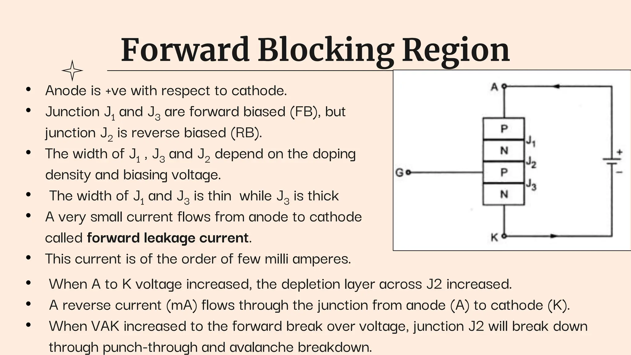
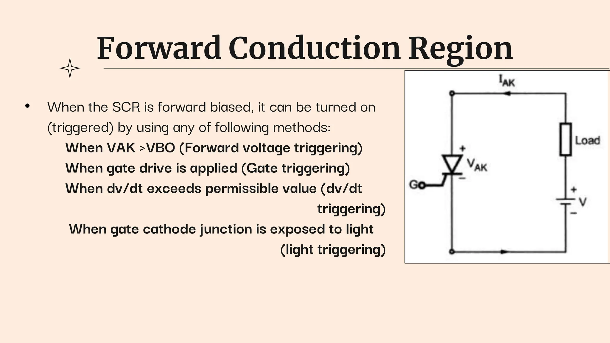
SlideShare a Scribd company logo
1 of 71
Download to read offline
Power Electronics
Power Semi- Conductor Devices
D.Poornima,
Assistant Professor (Sr.Gr),
Department of EEE,
Sri Ramakrishna Institute of Technology, Coimbatore
What is Power Electronics?
Power Electronics Combine:
Power –Static and rotating power equipment for
generation, transmission and distribution of power
Electronics –Solid state devices and circuits for
signal processing to meet desired control objectives
Control –steady state and dynamic characteristics
of a closed loop system
POWER ELECTRONICS –The applications of solid
state electronics for the control and conversion of
electric power
Primary Work of Power
Electronics
Process and control the flow of electrical energy by providing voltages
and currents in a form optimally suited for consumer demands
Applications of Power Electronics
Pic Courtesy: By Baltic Cable AB - http://www.balticcable.com/pdf/converter.pdf, CC BY-
SA 3.0, https://commons.wikimedia.org/w/index.php?curid=14126289
Applications of Power Electronics
What are Power Semiconductor Devices?
• Devices used as switches or rectifiers in power electronic circuits
• Can withstand large voltage across them during OFF state
• Has high current capability during ON state
• Types
SCR (Silicon Controlled Rectifier)
TRIAC (Three terminal diode for AC current)
GTO (Gate Turn-Off thyristor)
BJT (Bipolar Junction Transistor)
MOSFET (Metal Oxide Semiconductor Field Effect Transistor)
IGBT (Insulated Gate Bipolar Transistor)
IGCT (integrated gate-commutated thyristor )
Silicon Controlled Rectifier (SCR)
• Most commonly used thyristor.
• Used in almost all of the power converters.
• Attractive device for controlled rectifiers (AC-DC converters)
• Mainly lack in switching speeds compared to power transistors.
• Have high power handling capabilities.
• Drive requirements are also simple compared to power transistors.
• Called so as Silicon is used for its construction and its operation as a rectifier can be
controlled
• It is a unidirectional device – blocks current flow from cathode to anode
• Can be turned OFF by natural commutation and forced commutation.
• Commutation circuit for thyristor is bulky and expensive.
• Thyristors can be used as switching device up to about 1 kHz.
Construction of SCR
• Three terminals Device : Anode (A),
Cathode (K) and Gate (G)
• Four layer PNPN switching device with
alternate layers of P and N semiconductor
materials.
• There are three junctions namely J1, J2 and
J3
Symbol of
thyristor
Structure of thyristor
• The P1 and N2 semiconductor layers
are heavily doped.
• The width of N2 is very small about
10 mm
• Width of N1 is large about 50 to 100
mm but most lightly doped about
1014 cm–3.
• The width of P1 layer is 30 to 50 mm
• Width of P2 is about 30 to 100 mm.
• SCRs of voltage rating 10kV and an
rms current rating of 3000A and
power handling capability of 30MW
are available
SCR Working/VI Characteristics
• The working of the SCR can be discussed into three modes :
Reverse blocking mode
Forward blocking mode
Forward conduction mode.
• Fig. shows the V-I characteristics of the SCR.
• The characteristics shown in this are called static characteristics.
• The anode to cathode current IAK is plotted with respect to anode to cathode
voltage VAK.
• The voltage VBO is the forward break over voltage.
• VBR is the reverse break-down voltage.
• Ig1, Ig2, Ig3 are the gate currents applied to the SCR.
Reverse Blocking Region/Mode
• Anode is -ve with respect to cathode, gate is open
• Junction J1 and J3 are reverse biased (RB), but
junction J2 is forward biased (FB)- does not
conduct
• The width of J1 and J3 is thin while J3 is thick
• A very small current flows from cathode to anode
called reverse leakage current.
• At reverse break down voltage (VBR), the reverse
current increases rapidly.
• Large power dissipation also takes place in the thyristor.
• Due to dissipation, the junction temperature exceeds the permissible value and the SCR
is damaged.
• Reverse voltage across the SCR should never exceed V .
Forward Blocking Region
• Anode is +ve with respect to cathode.
• Junction J1 and J3 are forward biased (FB), but
junction J2 is reverse biased (RB).
• The width of J1 , J3 and J2 depend on the doping
density and biasing voltage.
• The width of J1 and J3 is thin while J3 is thick
• A very small current flows from anode to cathode
called forward leakage current.
• This current is of the order of few milli amperes.
• When A to K voltage increased, the depletion layer across J2 increased.
• A reverse current (mA) flows through the junction from anode (A) to cathode (K).
• When VAK increased to the forward break over voltage, junction J2 will break down
through punch-through and avalanche breakdown.
Forward Conduction Region
• When the SCR is forward biased, it can be turned on
(triggered) by using any of following methods:
When VAK >VBO (Forward voltage triggering)
When gate drive is applied (Gate triggering)
When dv/dt exceeds permissible value (dv/dt
triggering)
When gate cathode junction is exposed to light
(light triggering)
Forward Conduction Region (1)
When VAK >VBO
• When VAK >VBO (forward break-over voltage), the SCR is
driven in forward conduction even if gate is open.
• Junction J2 is reverse biased during forward blocking
mode ,When VAK exceeds VBO, the avalanche break-
down of junction J2 takes place.
• Anode to cathode voltage falls to very small value (2V).
• The dotted line in VI graph indicates switching of SCR
from forward blocking state (i.e. OFF) to forward
conduction state (i.e. ON).
• Heavy anode to cathode current flows and is only limited by the load.
IAK = V/load
Forward Conduction Region (2)
When gate drive is applied
• A +ve gate to cathode signal is applied whenever
the SCR is to be driven into forward conduction
mode (ON state).
• Also called gate triggering of the SCR.
• During forward blocking mode when gate signal is
applied, current flows from gate to cathode.
• This current adds to the forward leakage current.
• Avalanche break-down of junction J2 takes place
Thus SCR is driven into forward conduction mode
(ON state) even if VAK < VBO.
• VI characteristics of SCR shows the characteristic by centre (-.-.-.-.) lines.
Forward Conduction Region(2.1)
When gate drive is applied
• when gate drive current is increased, the SCR
turns-on at lower and lower values of anode to
cathode voltages less than VBO.
• Most convenient way of triggering the SCR.
• Once the thyristor goes into forward conduction
mode, the gate has no control over the conduction
of thyristor.
• The current IAK is only limited by the load, i.e.,
IAK = V/load
Forward Conduction Region(3)
When dv/dt exceeds permissible value
• dv/dt is the rate of change of anode to cathode voltage
with respect to time.
• In forward blocking state, an equivalent internal capacitor
is formed inside the SCR from anode to gate and gate to
cathode.
• Whenever the voltage applied across the SCR changes
rapidly, a transient current flows through the SCR due to
the internal capacitance.
• This current adds to the forward leakage current.
• And hence the SCR turns on even if VAK < VBO or gate drive is not applied.
Forward Conduction Region(3.1)
When dv/dt exceeds permissible value
• The dv/dt turn-on makes false triggering (unwanted) of
the SCR.
• Never used for triggering.
• Every SCR has dv/dt rating expressed in volts per
microseconds (V/μs).
• The voltage variations across the SCR must be kept
less than permissible value of dv/dt to avoid false
triggering.
• A small resistance is connected between gate and
cathode to avoid false triggering of SCR due to dv/dt.
• This resistance acts as a external path for leakage
current generated by the internal capacitor.
Forward Conduction Region(4)
When a gate cathode junction is exposed to light
• When the gate cathode junction is exposed to a beam of light, the current
flows in the junction due to photons of light.
• This current acts as a gate drive to the SCR and it is driven into conduction.
• This type of triggering is normally used in light activated SCRs (LASCR).
Important terms of SCR
Latching Current (IL)
• Latching current is the minimum
forward current that flows through
the SCR to keep it in forward
conduction mode (i.e. ON state) at
the time of triggering.
• If the current through the SCR is
less than latching current, then the
SCR goes back into forward
blocking state as soon as gate drive
is removed. .
Important terms of SCR
HOLDING CURRENT (IH)
• Consider that the SCR is in forward
conduction state (i.e. ON state).
• The SCR goes into forward blocking
state when current through it falls
below holding current
• i.e., IAK < IH; SCR turns-off.
• Holding current is the minimum
forward current that flows through
the SCR to keep it in forward
conduction mode during turn off.
• The holding current of the SCRs is
of the order of 8 to 10 milli amperes.
TWO TRANSISTOR MODEL OF SCR
• Middle two layers are split into two separate parts
• Two transistors are formed.
• Transistor T1 is pnp, whereas T2 is npn.
• Base of T1 is connected to collector of T2.
• Base of T2 is connected to collector of T1.
• Transistors are in common base configuration.
• When the SCR is forward biased and gate is open, various currents
flow
• Anode to cathode current is ID.
TWO TRANSISTOR MODEL OF SCR
• The collector current, emitter current and leakage currents of T1 are related as
• ICO is the reverse leakage current of the reverse biased junction J2.
• And α1 is the common base current gain of T1, and α2 is common base current gain of
T2.
TWO TRANSISTOR MODEL OF SCR
• When forward voltage is small, (α1 + α2) is very small and less than 1.
• Forward blocking current is also small.
• As forward voltage applied across the SCR increases, the values of α1 and α2 also
increase.
• When (α1 + α2) tends unity, then ID approaches infinity and the SCR goes into forward
conduction (ON-state) mode.
• The current through the SCR is only limited by the external load.
• Once the SCR goes into conduction, the two transistor model is no more applicable.
• The internal regeneration (Turning ON) takes place in the SCR due to avalanche
breakdown of reverse biased junction J2.
• When the current through the SCR falls below holding current, the forward blocking
state is regained.
• Then α1 and α2 of transistors are also reduced to small values.
TWO TRANSISTOR MODEL OF SCR
• When gate current Ig is applied, then equation (1) becomes
• ID is increased due to gate drive (Ig).
• ID flows through junction J2 and its avalanche break-down occurs at lower forward
voltage.
• With the gate drive, the SCR is turned on at voltages less than VBO.
• Gate becomes convenient way of triggering the SCR.
• Once the SCR is turned-on, the gate has no control over its conduction.
TRIAC
Introduction
• SCR is a unidirectional device
• In some applications, particularly in ac circuit, the
bidirectional current flow is required.
• Two thyristors are connected back to back or two anti-
parallel thyristors can be integrated into a single chip
• This device is called a TRIAC (triode ac switch)
• Bidirectional thyristor
• Extensively used for ac controller circuits.
• Name is derived by combining the capital letters from the
words TRIode and AC.
• Has three terminals - MT1, MT2 and gate G.
• MT1 is the reference point to measure voltages and currents
at gate terminal and MT2.
• The gate G is present near MT1
Construction
• It consists of three terminals
namely, main terminal 1 (MT1),
main terminal 2 (MT2), and
gate terminal G
• The cross hatched strip shows
that G is connected to N3 as
well as P2
• MT1 is connected to P2 and N2
• MT2 is connected to P1 and N4
TRIAC Working / VI Characteristics
• Operation of TRAIC resembles thyristor.
• When the voltage is applied, it will not conduct unless the voltage does not
exceed the break over voltage VBO or a gate pulse is applied.
• Can be turned on by applying a +ve or –ve voltage to the gate w.r.t. terminal MT1
• MT1 is taken as the point for measuring the voltage and current at the gate and
MT2 terminals
• Depending on the gate pulse and biasing condition, TRIAC conducts in four
different operating modes
 Mode 1: MT2 positive and positive gate current
 Mode 2: MT2 positive and gate current
 Negative
 Mode 3: MT2 negative, positive gate current
 Mode 4: MT2 negative and negative gate current
Mode 1:MT2 positive and positive gate current
• When MT2 is +ve w.r.t MT1, junctions J3 , J1 are FB and J2 is RB.
• When the gate terminal is +ve w.r.t MT1, the gate current is +ve. flows
from gate to MT1 through J1 (P2 N2)
• This device will turn on just like an SCR, but the gate current
• requirement is greater
• Due to contacts of gate and MT1 on P2 layer, some gate current flows
from the gate to MT1 through the P2 N2 (J1)
• P2 layer is flooded by electrons due to gate current and loses its
identity as P layer
• These electrons diffuse the junction J2 and collected at N1
• Reverse Bias junction N1P2 (J2) break downs
Mode 1:MT2 positive and positive gate current
• Then the structure operates as P1N1P2N2
• Under this condition, the TRIAC operates in first quadrant.
• There are two transistors and this makes TRIAC very sensitive
Mode 2:MT2 positive and negative gate current
• When MT2 is +ve and gate terminal is -ve w.r.t MT1
• Gate current flows through P2-N3 (J1)
• P2 layer is flooded by electrons due to gate current and loses its
identity as P layer
• These electrons diffuse the junction J2 and collected at N1
• Reverse Bias junction N1P2 (J2) break downs
• P1N1P2N3 structure start to conduct.
Mode 2:MT2 positive and negative gate current
• As the Ig rises, potential of P2N3 junction
rises towards the anode potential of MT1.
• As the right hand portion of P2 is
clamped at the potential of MT1, a
potential gradient exists across P2, its
left-hand region being at higher potential
than its right hand region.
• A current is established in layer P2 from
left to right which forward biased P2N2
junction and finally P1N1P2N2 structure
starts to conduct.
• The turn-ON process of Mode 2 is less
sensitive compared Mode1.
Mode 3:MT2 negative and positive gate current
• When MT2 is -ve w.r.t MT1, the device will be turn on by applying a +ve
gate voltage across gate and MT1.
• The device operates in third quadrant when it is turned ON.
• J4 is FB , electrons are injected into the P2 layer, loses its identity
Mode 3:MT2 negative and positive gate current
• The main structure P2N1P1N4 with N2 acting as a remote gate conducts.
• The gate current forward biases P2N2 junction.
• Layer N2 injects electrons into P2 layer
• The electrons from N2 are collected by P2N1 junction
• The holes are injected from P2, diffuse through N1 and reach at P1.
• A positive space charge builds up in the P1 region and more electrons from
N4 diffuse into P1 to neutralise the positive space charge region.
• These electrons reach at junction J2.
• They generate a negative space charge in the N1 region.
• Then more holes are injected from P2 into N1 and the regenerative process
continues until the P2N1P1N4 completely turned ON.
Mode 4:MT2 negative and negative gate current
• In this mode, N3 acts as a remote
gate.
• P2N3 (J1) junction is FB and
electrons are injected from N3 to
P2
• These electrons are collected by
P2N1 cause an increase of current
across P1N1.
• Structure P2N1P1N4 turns ON by
the regenerative action and the
device turns ON
Applications
• Since there are two conducting paths from MT2 to MT1 and MT1 to MT2
and the semiconductor layers interact with each other in the structure of
TRIAC, the voltage, current and frequency ratings are much less than
thyristors.
• Presently TRIACs are available with voltage rating 1200 V and current
rating 300 A.
• TRIACs are extensively used in lamp dimmers, heat control and speed
control of single phase ac motors.
VI Characteristics of TRIAC
• TRIAC can conduct in both the
directions
• It operates in the first and third
quadrant
• In I quadrant, MT2 is +ve with respect
to MT1 and in III quadrant, MT1 is +ve
with respect to MT2.
• When no gate pulse is applied, the
TRIAC can block the both half cycles of
the ac applied voltage
• Peak voltage across MT1 and MT2 is
always less than break over voltage in
both directions.
Gate Turn-Off Transistor
(GTO)
Introduction • GTO is just like a conventional thyristor but the turn-
OFF feature is incorporated within the device
• When +ve gate current applied in between gate and
cathode - device will be turned ON
• When -ve gate current is applied to gate-cathode-will
be turned OFF.
• Due to self-turned OFF capability, GTO is most
suitable device for inverters and choppers.
• Compact and cheap as no forced commutation
circuitry is needed
• But the -ve gate current requirement to turn off a GTO
is quite a large percentage of forward current.
Your Footer Here 45
Structure of GTO
• GTO is almost similar to SCR.
• But there are significant differences like:
• Gate and cathodes are highly
interdigitated
• There are n+ regions at regular intervals
in the p+ anode layer.
• This n+ layer makes direct contact with
n- layer.
• This is called anode short.
• This speeds up the turn-off mechanism
of GTO.
Your Footer Here 46
Working of GTO
During TURN ON,
• When the GTO is forward biased and the applied
forward voltage VAK is less than the forward breakover
voltage VBRF, GTO operates in off condition and the
device is said to be in the forward blocking mode.
• To turn ON the device, a gate current is injected through
gate terminal
• When a positive gate current is given, holes are injected
into the P region (cathode region)
Your Footer Here 47
Working of GTO
During TURN ON,
• This results in the emission of electrons from the
cathode towards the anode terminal
• This in turn induces hole injection from the anode
terminal into the base region.
• This will continue till the GTO turns on
Your Footer Here 48
Working of GTO
During TURN OFF,
• A reverse bias is applied at the gate by making the gate
-ve w.r.t cathode.
• A part of the holes from the P base layer is extracted
through the gate which suppress the injection of
electrons from the cathode.
• In response to this, more hole current is extracted
through the gate results more suppression of electrons
from the cathode.
• Eventually, the voltage drop across the
p base junction causes to reverse bias
the gate cathode junction
• GTO is turned OFF.
Your Footer Here 49
BIPOLAR JUNCTION TRANSISTOR
Introduction
• A Bipolar Junction Transistor (also known as a BJT or BJT Transistor) is a three-
terminal semiconductor device
• It is a current controlled device.
• The three terminals of the BJT are the base, the collector and the emitter.
• Called bipolar as it uses both electrons and holes as charge carriers.
• It can be used as a switch in digital electronics or as an amplifier
in analog electronics.
• Nowadays, field-effect transistors are widely used in electronics applications but still,
BJTs are quite extensively used
• There are two types of BJTs –
– NPN transistors
– PNP transistors
Structure of BJT
• n-p-n power transistor is a four layer n+ p n– n+ structure.
• Three terminals such as collector (C), base (B) and emitter (E).
• Base is used as an input terminal,
collector is used as output terminal.
• In common emitter configuration,
emitter is common between input and
output terminals.
• The width of emitter, n+ layer is
about 10 µm and doping intensity
is NA = 1019 cm–3.
• Base thickness or width of p layer
is about 5 to 20 mm and the
doping density is NA = 1016 cm–3.
Structure of BJT
• The width of n– layer or collector drift region is about 50mm to 200mm
• Doping density is minimum in drift
region and its value is about
NA = 1014 cm–3.
• The width of n+ collector region is
maximum and it is about 250 mm.
• The doping density of N + type
semiconductor layer is NA = 1019cm–3
• The base thickness is as small as
possible to provide good amplification
• But due to this, breakdown voltage
capability of BJT is reduced.
• So, base thickness is made more than
logic level transistors to increase
breakdown voltage capability.
WORKING OF BJT
• When no battery is connected between the transistor terminals, it is said to be in
unbiased state or open-circuit state
• The process of applying dc voltages across the different terminals of the transistor
is called Biasing
• For normal operation, emitter-base junction is always forward biased and
collector-base junction is reverse biased
• Forward bias at EB junction reduces the barrier
potential-narrows the depletion region
• CB junction produces a wide depletion region due to
reverse bias
• This produces a very narrow effective base width Wb
•
WORKING OF BJT……
• Electrons are injected into the emitter region by the emitter bias supply VEB
• This makes the electron concentration in emitter junction very large
• Some of these electrons combine with the holes in the P-type base (1-5%)
• Electron concentration in collector junction is small
• Since base width is less, the gradient of electron concentration is very large in base
• This causes the diffusion of electrons from emitter to collector
• For each electron combined in the base region,
an electron leaves the region via base terminal and
causes a small base current
• The emitter current is equal to the base and collector current.
IE =IC + IB
•The ratio between dc collector and dc emitter current is known as dc alpha or (𝛼DC).
αDC = IC/IE
• Value of αDC is from 0.95 to 0.99 or larger but it remains always less than one.
• The dc current gain of transistor is the ratio between dc collector and dc base current,
denoted as (βDC).
(βDC)= IC /IB
WORKING OF BJT……
Metal Oxide Semiconductor Field Effect
Transistor(MOSFET)
INTRODUCTION
• MOSFET is a three terminal (source, gate and drain) device and drain
current in it is also controlled by gate bias.
• Voltage-controlled device.
• Unipolar device as current through it depends upon the majority
carriers.
• Gate terminal is the control terminal, where the gate current is low.
• Gate circuit impedance is very large which permits it to be driven
directly from the microelectronics circuit.
• Applicable for low-power high-frequency converters.
• Two types
• n-channel enhancement type
• p-channel enhancement type
• On P-substrate two heavily doped n+ regions are diffused
• An insulating layer of silicon dioxide (SiO2)is grown on the surface.
• This insulating layer is etched in order to embed metallic sources and drain
terminals.
• n+ regions make contact with the source and drain terminal as shown.
• A layer of metal is also deposited on SiO2 so as to form the gate of MOSFET.
• GATE circuit decides the state of MOSFET.
• When the gate circuit is open the current
through the MOSFET (drain to source) is zero.
• Because one n+-p reverse biased.
• The Load is connected between the drain and
source.
Structure of MOSFET
OPERATIONOFDE-MOSFET(Gateismade+ve)
• DE-MOSFETcanbeoperatedwith eithera+veora -vegate.
• When gate is +ve with respect to the source it operates in the enhancement—or E-mode and when the gate is
negative with respectto the source,itoperates indepletion-mode.
• When the drain is made +ve with respect to source, a drain current will flow, even with zero gate potential and the
MOSFETissaidto beoperating inE-mode.
• Inthis mode,gate attracts thenegativechargecarriersfromthe P-
substrate to theN-channel
• Itreducesthechannelresistanceandincreasesthedrain-current.
• Themore+vethegateis made,themoredraincurrentflows.
Insulated Gate Bipolar Transistor
(IGBT)
Introduction • The IGBT is the combination of BJT and MOSFET.
• Insulated Gate refers to the input part of MOSFET
having very high input impedance.
• It does not draw any input current rather it operates
on the voltage at its gate terminal.
• “Bipolar” refers the current flow is due to both types
of charge carriers.
• Can handle very large currents and voltages using
small voltage signals.
• This hybrid combination makes the IGBT a voltage-
controlled device.
Your Footer Here 62
Structure of IGBT
• Four-layer PNPN device having three PN junctions.
• It has three terminals Gate (G), Collector(C) and Emitter (E).
• Gate terminal as it is the input part,
taken from MOSFET while the collector
and emitter as they are the output,
taken from the BJT.
• Emitter and gate are metal electrodes.
• Emitter is directly attached to the N+
region while the gate is insulated using a
silicon dioxide layer.
Your Footer Here 63
Structure of IGBT
• The base P+ layer inject holes into N-layer
• It is called injector layer.
• The N- layer is called the drift region.
• Its thickness is proportional to voltage blocking capacity.
• The P layer above is known as the body of IGBT.
• The N- layer is designed to have a path for current flow between E and
C through the junction using the channel that is created under the
influence of the voltage at the gate electrode.
Your Footer Here 64
Working
• Collector (C) and emitter (E) terminals are used for the conduction
• Gate (G) is used for controlling the IGBT.
• Working is based on the biasing between Gate-Emitter terminals and Collector-
Emitter terminals.
• Collector is kept at a positive voltage than the emitter.
• Junction J1 is FB and J2 becomes RB and there is no voltage at the gate.
• Due to reverse J2, the IGBT remains switched off, no current will flow between
collector and emitter.
Your Footer Here 65
Working
• Applying a +ve gate voltage VG, -ve charges will accumulate right beneath the SiO2-
layer due to capacitance.
• Increasing the VG increases the number of charges - eventually form a layer when
the VG exceeds the threshold voltage, in the upper P-region.
• This layer form N-channel that shorts N- drift region and N+ region.
• The electrons from the emitter flow from N+ region into N- drift region.
• While the holes from the collector are injected from the P+ region into the N- drift
region.
• Due to the excess of both electrons and holes in the drift region, its conductivity
increases and starts the conduction of current.
• Hence the IGBT switches ON.
Your Footer Here 66
Integrated Gate-Commutated
Thyristor (IGCT)
Introduction
• Is a power semiconductor electronic device, used for switching electric current in industrial
equipment.
• It is related to the gate turn-off (GTO) thyristor.
• Fully controllable power switch - it can be turned both on and off by its
control terminal (the gate).
• Lower conduction losses as compared to GTO thyristors.
• Withstands higher rates of voltage rise(dv/dt) - snubber circuits are not required for most
of the applications.
• Much faster turn-off times compared to the GTO’s - operate at higher frequencies—up to
several kHz for very short periods of time.
• High switching losses - operating frequency limited up to 500 Hz.
Construction
• It is made of the integration of the gate unit with
the Gate Commutated Thyristor (GCT) wafer
device.
• The close integration ensures fast commutation
• The structure is very similar to a GTO
• The main differences are
reduction in cell size,
much more substantial gate
connection
• Lower inductance in the gate drive circuit and
drive circuit connection due to
large contact area
short distance
Construction
• The very high gate currents and fast dI/dt rise of
the gate current mean that regular wires can not
be used to connect the gate drive to the IGCT.
• The drive circuit PCB is integrated into the
package of the device.
• The drive circuit surrounds the device and a large
circular conductor attaching to the edge of the
IGCT is used.
• The large contact area and short distance reduce
both the inductance and resistance of the
connection.
CREDITS: This presentation template was created by Slidesgo, including icons
by Flaticon, infographics & images by Freepik
Thanks!

More Related Content

Similar to Power Electronics- Power Semiconductor devices.pptx

PE4MSc_Ch1_SC_devices.pptx
PE4MSc_Ch1_SC_devices.pptxPE4MSc_Ch1_SC_devices.pptx
PE4MSc_Ch1_SC_devices.pptxAddisuMengesha2
 
Silicon controlled rectifier ( SCR )
Silicon controlled rectifier ( SCR )Silicon controlled rectifier ( SCR )
Silicon controlled rectifier ( SCR )DikshaTripathi20
 
62-power-semiconductor-devices.ppt
62-power-semiconductor-devices.ppt62-power-semiconductor-devices.ppt
62-power-semiconductor-devices.pptMdSazibMollik
 
62-power-semiconductor-devices.pptx
62-power-semiconductor-devices.pptx62-power-semiconductor-devices.pptx
62-power-semiconductor-devices.pptxyogeshkute7
 
62-power-semiconductor-devices.ppt
62-power-semiconductor-devices.ppt62-power-semiconductor-devices.ppt
62-power-semiconductor-devices.pptssuser7598a2
 
62-power-semiconductor-devices (1).ppt
62-power-semiconductor-devices (1).ppt62-power-semiconductor-devices (1).ppt
62-power-semiconductor-devices (1).pptGodspower Bruno, GMNSE
 
62-power-semiconductor-devices.pptx
62-power-semiconductor-devices.pptx62-power-semiconductor-devices.pptx
62-power-semiconductor-devices.pptxyogeshkute
 
Silicon Controlled Rectifier
Silicon Controlled Rectifier Silicon Controlled Rectifier
Silicon Controlled Rectifier Nikhil Kumar
 
NEW THYRISTOR.ppt
NEW THYRISTOR.pptNEW THYRISTOR.ppt
NEW THYRISTOR.pptyogeshkute7
 
Power semiconductor devices ppt new converted
Power semiconductor devices ppt new convertedPower semiconductor devices ppt new converted
Power semiconductor devices ppt new convertedPallavi Choudekar
 
SCR unit II.pptx
SCR unit II.pptxSCR unit II.pptx
SCR unit II.pptxyogeshkute
 
l2-power semiconductor devices and charactoristics.ppt
l2-power semiconductor devices and charactoristics.pptl2-power semiconductor devices and charactoristics.ppt
l2-power semiconductor devices and charactoristics.pptantexnebyu
 
Power Electronics
Power ElectronicsPower Electronics
Power ElectronicsMirza Baig
 

Similar to Power Electronics- Power Semiconductor devices.pptx (20)

Thyristor
Thyristor Thyristor
Thyristor
 
PE4MSc_Ch1_SC_devices.pptx
PE4MSc_Ch1_SC_devices.pptxPE4MSc_Ch1_SC_devices.pptx
PE4MSc_Ch1_SC_devices.pptx
 
Lecture slides_power electronics daniel hart Ch1.pdf
Lecture slides_power electronics daniel hart Ch1.pdfLecture slides_power electronics daniel hart Ch1.pdf
Lecture slides_power electronics daniel hart Ch1.pdf
 
Silicon controlled rectifier ( SCR )
Silicon controlled rectifier ( SCR )Silicon controlled rectifier ( SCR )
Silicon controlled rectifier ( SCR )
 
POWER ELECTRONICS
POWER ELECTRONICSPOWER ELECTRONICS
POWER ELECTRONICS
 
62-power-semiconductor-devices.ppt
62-power-semiconductor-devices.ppt62-power-semiconductor-devices.ppt
62-power-semiconductor-devices.ppt
 
62-power-semiconductor-devices.ppt
62-power-semiconductor-devices.ppt62-power-semiconductor-devices.ppt
62-power-semiconductor-devices.ppt
 
62-power-semiconductor-devices.pptx
62-power-semiconductor-devices.pptx62-power-semiconductor-devices.pptx
62-power-semiconductor-devices.pptx
 
62-power-semiconductor-devices.ppt
62-power-semiconductor-devices.ppt62-power-semiconductor-devices.ppt
62-power-semiconductor-devices.ppt
 
62-power-semiconductor-devices (1).ppt
62-power-semiconductor-devices (1).ppt62-power-semiconductor-devices (1).ppt
62-power-semiconductor-devices (1).ppt
 
62-power-semiconductor-devices.pptx
62-power-semiconductor-devices.pptx62-power-semiconductor-devices.pptx
62-power-semiconductor-devices.pptx
 
Silicon Controlled Rectifier
Silicon Controlled Rectifier Silicon Controlled Rectifier
Silicon Controlled Rectifier
 
NEW THYRISTOR.ppt
NEW THYRISTOR.pptNEW THYRISTOR.ppt
NEW THYRISTOR.ppt
 
IGBT
IGBTIGBT
IGBT
 
Power semiconductor devices ppt new converted
Power semiconductor devices ppt new convertedPower semiconductor devices ppt new converted
Power semiconductor devices ppt new converted
 
SCR unit II.pptx
SCR unit II.pptxSCR unit II.pptx
SCR unit II.pptx
 
Power Electronics
Power ElectronicsPower Electronics
Power Electronics
 
Thyristors.pptx
Thyristors.pptxThyristors.pptx
Thyristors.pptx
 
l2-power semiconductor devices and charactoristics.ppt
l2-power semiconductor devices and charactoristics.pptl2-power semiconductor devices and charactoristics.ppt
l2-power semiconductor devices and charactoristics.ppt
 
Power Electronics
Power ElectronicsPower Electronics
Power Electronics
 

More from Poornima D

Power Electronics - Phase Controlled Converters.pptx
Power Electronics - Phase Controlled Converters.pptxPower Electronics - Phase Controlled Converters.pptx
Power Electronics - Phase Controlled Converters.pptxPoornima D
 
Power Electronics- More about Devices.pptx
Power Electronics- More about Devices.pptxPower Electronics- More about Devices.pptx
Power Electronics- More about Devices.pptxPoornima D
 
UEEC010 - Uncontrolled rectifiers.pptx
UEEC010 - Uncontrolled rectifiers.pptxUEEC010 - Uncontrolled rectifiers.pptx
UEEC010 - Uncontrolled rectifiers.pptxPoornima D
 
Power Electronics introduction
Power Electronics introductionPower Electronics introduction
Power Electronics introductionPoornima D
 
Medical instrumentation- cardiac arrhythmia, pacemaker, defibrillator
Medical instrumentation- cardiac arrhythmia, pacemaker, defibrillatorMedical instrumentation- cardiac arrhythmia, pacemaker, defibrillator
Medical instrumentation- cardiac arrhythmia, pacemaker, defibrillatorPoornima D
 
medical instrumentation- blood flow rate and plethysmograph
medical instrumentation- blood flow rate and plethysmographmedical instrumentation- blood flow rate and plethysmograph
medical instrumentation- blood flow rate and plethysmographPoornima D
 
Medical instrumentation- patient monitoring systems
Medical instrumentation- patient monitoring systems Medical instrumentation- patient monitoring systems
Medical instrumentation- patient monitoring systems Poornima D
 
Medical Instrumentation- body parameters measurement
Medical Instrumentation- body parameters measurementMedical Instrumentation- body parameters measurement
Medical Instrumentation- body parameters measurementPoornima D
 
Medical Instrumentation- EMG,ERG,EOG,PCG
Medical Instrumentation- EMG,ERG,EOG,PCGMedical Instrumentation- EMG,ERG,EOG,PCG
Medical Instrumentation- EMG,ERG,EOG,PCGPoornima D
 
Medical Instrumentation- Biosignals, ECG
Medical Instrumentation- Biosignals, ECGMedical Instrumentation- Biosignals, ECG
Medical Instrumentation- Biosignals, ECGPoornima D
 
Medical Instrumentation- EEG
Medical Instrumentation- EEGMedical Instrumentation- EEG
Medical Instrumentation- EEGPoornima D
 
Biomedical Instrumentation introduction, Bioamplifiers
Biomedical Instrumentation introduction, BioamplifiersBiomedical Instrumentation introduction, Bioamplifiers
Biomedical Instrumentation introduction, BioamplifiersPoornima D
 

More from Poornima D (12)

Power Electronics - Phase Controlled Converters.pptx
Power Electronics - Phase Controlled Converters.pptxPower Electronics - Phase Controlled Converters.pptx
Power Electronics - Phase Controlled Converters.pptx
 
Power Electronics- More about Devices.pptx
Power Electronics- More about Devices.pptxPower Electronics- More about Devices.pptx
Power Electronics- More about Devices.pptx
 
UEEC010 - Uncontrolled rectifiers.pptx
UEEC010 - Uncontrolled rectifiers.pptxUEEC010 - Uncontrolled rectifiers.pptx
UEEC010 - Uncontrolled rectifiers.pptx
 
Power Electronics introduction
Power Electronics introductionPower Electronics introduction
Power Electronics introduction
 
Medical instrumentation- cardiac arrhythmia, pacemaker, defibrillator
Medical instrumentation- cardiac arrhythmia, pacemaker, defibrillatorMedical instrumentation- cardiac arrhythmia, pacemaker, defibrillator
Medical instrumentation- cardiac arrhythmia, pacemaker, defibrillator
 
medical instrumentation- blood flow rate and plethysmograph
medical instrumentation- blood flow rate and plethysmographmedical instrumentation- blood flow rate and plethysmograph
medical instrumentation- blood flow rate and plethysmograph
 
Medical instrumentation- patient monitoring systems
Medical instrumentation- patient monitoring systems Medical instrumentation- patient monitoring systems
Medical instrumentation- patient monitoring systems
 
Medical Instrumentation- body parameters measurement
Medical Instrumentation- body parameters measurementMedical Instrumentation- body parameters measurement
Medical Instrumentation- body parameters measurement
 
Medical Instrumentation- EMG,ERG,EOG,PCG
Medical Instrumentation- EMG,ERG,EOG,PCGMedical Instrumentation- EMG,ERG,EOG,PCG
Medical Instrumentation- EMG,ERG,EOG,PCG
 
Medical Instrumentation- Biosignals, ECG
Medical Instrumentation- Biosignals, ECGMedical Instrumentation- Biosignals, ECG
Medical Instrumentation- Biosignals, ECG
 
Medical Instrumentation- EEG
Medical Instrumentation- EEGMedical Instrumentation- EEG
Medical Instrumentation- EEG
 
Biomedical Instrumentation introduction, Bioamplifiers
Biomedical Instrumentation introduction, BioamplifiersBiomedical Instrumentation introduction, Bioamplifiers
Biomedical Instrumentation introduction, Bioamplifiers
 

Recently uploaded

Gurgaon ✡️9711147426✨Call In girls Gurgaon Sector 51 escort service
Gurgaon ✡️9711147426✨Call In girls Gurgaon Sector 51 escort serviceGurgaon ✡️9711147426✨Call In girls Gurgaon Sector 51 escort service
Gurgaon ✡️9711147426✨Call In girls Gurgaon Sector 51 escort servicejennyeacort
 
Past, Present and Future of Generative AI
Past, Present and Future of Generative AIPast, Present and Future of Generative AI
Past, Present and Future of Generative AIabhishek36461
 
Oxy acetylene welding presentation note.
Oxy acetylene welding presentation note.Oxy acetylene welding presentation note.
Oxy acetylene welding presentation note.eptoze12
 
Gfe Mayur Vihar Call Girls Service WhatsApp -> 9999965857 Available 24x7 ^ De...
Gfe Mayur Vihar Call Girls Service WhatsApp -> 9999965857 Available 24x7 ^ De...Gfe Mayur Vihar Call Girls Service WhatsApp -> 9999965857 Available 24x7 ^ De...
Gfe Mayur Vihar Call Girls Service WhatsApp -> 9999965857 Available 24x7 ^ De...srsj9000
 
GDSC ASEB Gen AI study jams presentation
GDSC ASEB Gen AI study jams presentationGDSC ASEB Gen AI study jams presentation
GDSC ASEB Gen AI study jams presentationGDSCAESB
 
Microscopic Analysis of Ceramic Materials.pptx
Microscopic Analysis of Ceramic Materials.pptxMicroscopic Analysis of Ceramic Materials.pptx
Microscopic Analysis of Ceramic Materials.pptxpurnimasatapathy1234
 
Internship report on mechanical engineering
Internship report on mechanical engineeringInternship report on mechanical engineering
Internship report on mechanical engineeringmalavadedarshan25
 
SPICE PARK APR2024 ( 6,793 SPICE Models )
SPICE PARK APR2024 ( 6,793 SPICE Models )SPICE PARK APR2024 ( 6,793 SPICE Models )
SPICE PARK APR2024 ( 6,793 SPICE Models )Tsuyoshi Horigome
 
CCS355 Neural Network & Deep Learning Unit II Notes with Question bank .pdf
CCS355 Neural Network & Deep Learning Unit II Notes with Question bank .pdfCCS355 Neural Network & Deep Learning Unit II Notes with Question bank .pdf
CCS355 Neural Network & Deep Learning Unit II Notes with Question bank .pdfAsst.prof M.Gokilavani
 
Heart Disease Prediction using machine learning.pptx
Heart Disease Prediction using machine learning.pptxHeart Disease Prediction using machine learning.pptx
Heart Disease Prediction using machine learning.pptxPoojaBan
 
Call Us ≽ 8377877756 ≼ Call Girls In Shastri Nagar (Delhi)
Call Us ≽ 8377877756 ≼ Call Girls In Shastri Nagar (Delhi)Call Us ≽ 8377877756 ≼ Call Girls In Shastri Nagar (Delhi)
Call Us ≽ 8377877756 ≼ Call Girls In Shastri Nagar (Delhi)dollysharma2066
 
Study on Air-Water & Water-Water Heat Exchange in a Finned Tube Exchanger
Study on Air-Water & Water-Water Heat Exchange in a Finned Tube ExchangerStudy on Air-Water & Water-Water Heat Exchange in a Finned Tube Exchanger
Study on Air-Water & Water-Water Heat Exchange in a Finned Tube ExchangerAnamika Sarkar
 
complete construction, environmental and economics information of biomass com...
complete construction, environmental and economics information of biomass com...complete construction, environmental and economics information of biomass com...
complete construction, environmental and economics information of biomass com...asadnawaz62
 
chaitra-1.pptx fake news detection using machine learning
chaitra-1.pptx  fake news detection using machine learningchaitra-1.pptx  fake news detection using machine learning
chaitra-1.pptx fake news detection using machine learningmisbanausheenparvam
 
Artificial-Intelligence-in-Electronics (K).pptx
Artificial-Intelligence-in-Electronics (K).pptxArtificial-Intelligence-in-Electronics (K).pptx
Artificial-Intelligence-in-Electronics (K).pptxbritheesh05
 
INFLUENCE OF NANOSILICA ON THE PROPERTIES OF CONCRETE
INFLUENCE OF NANOSILICA ON THE PROPERTIES OF CONCRETEINFLUENCE OF NANOSILICA ON THE PROPERTIES OF CONCRETE
INFLUENCE OF NANOSILICA ON THE PROPERTIES OF CONCRETEroselinkalist12
 
CCS355 Neural Network & Deep Learning UNIT III notes and Question bank .pdf
CCS355 Neural Network & Deep Learning UNIT III notes and Question bank .pdfCCS355 Neural Network & Deep Learning UNIT III notes and Question bank .pdf
CCS355 Neural Network & Deep Learning UNIT III notes and Question bank .pdfAsst.prof M.Gokilavani
 
IVE Industry Focused Event - Defence Sector 2024
IVE Industry Focused Event - Defence Sector 2024IVE Industry Focused Event - Defence Sector 2024
IVE Industry Focused Event - Defence Sector 2024Mark Billinghurst
 

Recently uploaded (20)

Gurgaon ✡️9711147426✨Call In girls Gurgaon Sector 51 escort service
Gurgaon ✡️9711147426✨Call In girls Gurgaon Sector 51 escort serviceGurgaon ✡️9711147426✨Call In girls Gurgaon Sector 51 escort service
Gurgaon ✡️9711147426✨Call In girls Gurgaon Sector 51 escort service
 
Past, Present and Future of Generative AI
Past, Present and Future of Generative AIPast, Present and Future of Generative AI
Past, Present and Future of Generative AI
 
Oxy acetylene welding presentation note.
Oxy acetylene welding presentation note.Oxy acetylene welding presentation note.
Oxy acetylene welding presentation note.
 
Gfe Mayur Vihar Call Girls Service WhatsApp -> 9999965857 Available 24x7 ^ De...
Gfe Mayur Vihar Call Girls Service WhatsApp -> 9999965857 Available 24x7 ^ De...Gfe Mayur Vihar Call Girls Service WhatsApp -> 9999965857 Available 24x7 ^ De...
Gfe Mayur Vihar Call Girls Service WhatsApp -> 9999965857 Available 24x7 ^ De...
 
GDSC ASEB Gen AI study jams presentation
GDSC ASEB Gen AI study jams presentationGDSC ASEB Gen AI study jams presentation
GDSC ASEB Gen AI study jams presentation
 
Microscopic Analysis of Ceramic Materials.pptx
Microscopic Analysis of Ceramic Materials.pptxMicroscopic Analysis of Ceramic Materials.pptx
Microscopic Analysis of Ceramic Materials.pptx
 
Internship report on mechanical engineering
Internship report on mechanical engineeringInternship report on mechanical engineering
Internship report on mechanical engineering
 
young call girls in Green Park🔝 9953056974 🔝 escort Service
young call girls in Green Park🔝 9953056974 🔝 escort Serviceyoung call girls in Green Park🔝 9953056974 🔝 escort Service
young call girls in Green Park🔝 9953056974 🔝 escort Service
 
POWER SYSTEMS-1 Complete notes examples
POWER SYSTEMS-1 Complete notes  examplesPOWER SYSTEMS-1 Complete notes  examples
POWER SYSTEMS-1 Complete notes examples
 
SPICE PARK APR2024 ( 6,793 SPICE Models )
SPICE PARK APR2024 ( 6,793 SPICE Models )SPICE PARK APR2024 ( 6,793 SPICE Models )
SPICE PARK APR2024 ( 6,793 SPICE Models )
 
CCS355 Neural Network & Deep Learning Unit II Notes with Question bank .pdf
CCS355 Neural Network & Deep Learning Unit II Notes with Question bank .pdfCCS355 Neural Network & Deep Learning Unit II Notes with Question bank .pdf
CCS355 Neural Network & Deep Learning Unit II Notes with Question bank .pdf
 
Heart Disease Prediction using machine learning.pptx
Heart Disease Prediction using machine learning.pptxHeart Disease Prediction using machine learning.pptx
Heart Disease Prediction using machine learning.pptx
 
Call Us ≽ 8377877756 ≼ Call Girls In Shastri Nagar (Delhi)
Call Us ≽ 8377877756 ≼ Call Girls In Shastri Nagar (Delhi)Call Us ≽ 8377877756 ≼ Call Girls In Shastri Nagar (Delhi)
Call Us ≽ 8377877756 ≼ Call Girls In Shastri Nagar (Delhi)
 
Study on Air-Water & Water-Water Heat Exchange in a Finned Tube Exchanger
Study on Air-Water & Water-Water Heat Exchange in a Finned Tube ExchangerStudy on Air-Water & Water-Water Heat Exchange in a Finned Tube Exchanger
Study on Air-Water & Water-Water Heat Exchange in a Finned Tube Exchanger
 
complete construction, environmental and economics information of biomass com...
complete construction, environmental and economics information of biomass com...complete construction, environmental and economics information of biomass com...
complete construction, environmental and economics information of biomass com...
 
chaitra-1.pptx fake news detection using machine learning
chaitra-1.pptx  fake news detection using machine learningchaitra-1.pptx  fake news detection using machine learning
chaitra-1.pptx fake news detection using machine learning
 
Artificial-Intelligence-in-Electronics (K).pptx
Artificial-Intelligence-in-Electronics (K).pptxArtificial-Intelligence-in-Electronics (K).pptx
Artificial-Intelligence-in-Electronics (K).pptx
 
INFLUENCE OF NANOSILICA ON THE PROPERTIES OF CONCRETE
INFLUENCE OF NANOSILICA ON THE PROPERTIES OF CONCRETEINFLUENCE OF NANOSILICA ON THE PROPERTIES OF CONCRETE
INFLUENCE OF NANOSILICA ON THE PROPERTIES OF CONCRETE
 
CCS355 Neural Network & Deep Learning UNIT III notes and Question bank .pdf
CCS355 Neural Network & Deep Learning UNIT III notes and Question bank .pdfCCS355 Neural Network & Deep Learning UNIT III notes and Question bank .pdf
CCS355 Neural Network & Deep Learning UNIT III notes and Question bank .pdf
 
IVE Industry Focused Event - Defence Sector 2024
IVE Industry Focused Event - Defence Sector 2024IVE Industry Focused Event - Defence Sector 2024
IVE Industry Focused Event - Defence Sector 2024
 

Power Electronics- Power Semiconductor devices.pptx

  • 1. Power Electronics Power Semi- Conductor Devices D.Poornima, Assistant Professor (Sr.Gr), Department of EEE, Sri Ramakrishna Institute of Technology, Coimbatore
  • 2. What is Power Electronics? Power Electronics Combine: Power –Static and rotating power equipment for generation, transmission and distribution of power Electronics –Solid state devices and circuits for signal processing to meet desired control objectives Control –steady state and dynamic characteristics of a closed loop system POWER ELECTRONICS –The applications of solid state electronics for the control and conversion of electric power
  • 3. Primary Work of Power Electronics Process and control the flow of electrical energy by providing voltages and currents in a form optimally suited for consumer demands
  • 4. Applications of Power Electronics
  • 5. Applications of Power Electronics
  • 6. Applications of Power Electronics Pic Courtesy: By Baltic Cable AB - http://www.balticcable.com/pdf/converter.pdf, CC BY- SA 3.0, https://commons.wikimedia.org/w/index.php?curid=14126289
  • 7. Applications of Power Electronics
  • 8. What are Power Semiconductor Devices? • Devices used as switches or rectifiers in power electronic circuits • Can withstand large voltage across them during OFF state • Has high current capability during ON state • Types SCR (Silicon Controlled Rectifier) TRIAC (Three terminal diode for AC current) GTO (Gate Turn-Off thyristor) BJT (Bipolar Junction Transistor) MOSFET (Metal Oxide Semiconductor Field Effect Transistor) IGBT (Insulated Gate Bipolar Transistor) IGCT (integrated gate-commutated thyristor )
  • 9. Silicon Controlled Rectifier (SCR) • Most commonly used thyristor. • Used in almost all of the power converters. • Attractive device for controlled rectifiers (AC-DC converters) • Mainly lack in switching speeds compared to power transistors. • Have high power handling capabilities. • Drive requirements are also simple compared to power transistors. • Called so as Silicon is used for its construction and its operation as a rectifier can be controlled • It is a unidirectional device – blocks current flow from cathode to anode • Can be turned OFF by natural commutation and forced commutation. • Commutation circuit for thyristor is bulky and expensive. • Thyristors can be used as switching device up to about 1 kHz.
  • 10. Construction of SCR • Three terminals Device : Anode (A), Cathode (K) and Gate (G) • Four layer PNPN switching device with alternate layers of P and N semiconductor materials. • There are three junctions namely J1, J2 and J3 Symbol of thyristor Structure of thyristor
  • 11. • The P1 and N2 semiconductor layers are heavily doped. • The width of N2 is very small about 10 mm • Width of N1 is large about 50 to 100 mm but most lightly doped about 1014 cm–3. • The width of P1 layer is 30 to 50 mm • Width of P2 is about 30 to 100 mm. • SCRs of voltage rating 10kV and an rms current rating of 3000A and power handling capability of 30MW are available
  • 12. SCR Working/VI Characteristics • The working of the SCR can be discussed into three modes : Reverse blocking mode Forward blocking mode Forward conduction mode. • Fig. shows the V-I characteristics of the SCR. • The characteristics shown in this are called static characteristics. • The anode to cathode current IAK is plotted with respect to anode to cathode voltage VAK. • The voltage VBO is the forward break over voltage. • VBR is the reverse break-down voltage. • Ig1, Ig2, Ig3 are the gate currents applied to the SCR.
  • 13.
  • 14. Reverse Blocking Region/Mode • Anode is -ve with respect to cathode, gate is open • Junction J1 and J3 are reverse biased (RB), but junction J2 is forward biased (FB)- does not conduct • The width of J1 and J3 is thin while J3 is thick • A very small current flows from cathode to anode called reverse leakage current. • At reverse break down voltage (VBR), the reverse current increases rapidly. • Large power dissipation also takes place in the thyristor. • Due to dissipation, the junction temperature exceeds the permissible value and the SCR is damaged. • Reverse voltage across the SCR should never exceed V .
  • 15. Forward Blocking Region • Anode is +ve with respect to cathode. • Junction J1 and J3 are forward biased (FB), but junction J2 is reverse biased (RB). • The width of J1 , J3 and J2 depend on the doping density and biasing voltage. • The width of J1 and J3 is thin while J3 is thick • A very small current flows from anode to cathode called forward leakage current. • This current is of the order of few milli amperes. • When A to K voltage increased, the depletion layer across J2 increased. • A reverse current (mA) flows through the junction from anode (A) to cathode (K). • When VAK increased to the forward break over voltage, junction J2 will break down through punch-through and avalanche breakdown.
  • 16. Forward Conduction Region • When the SCR is forward biased, it can be turned on (triggered) by using any of following methods: When VAK >VBO (Forward voltage triggering) When gate drive is applied (Gate triggering) When dv/dt exceeds permissible value (dv/dt triggering) When gate cathode junction is exposed to light (light triggering)
  • 17. Forward Conduction Region (1) When VAK >VBO • When VAK >VBO (forward break-over voltage), the SCR is driven in forward conduction even if gate is open. • Junction J2 is reverse biased during forward blocking mode ,When VAK exceeds VBO, the avalanche break- down of junction J2 takes place. • Anode to cathode voltage falls to very small value (2V). • The dotted line in VI graph indicates switching of SCR from forward blocking state (i.e. OFF) to forward conduction state (i.e. ON). • Heavy anode to cathode current flows and is only limited by the load. IAK = V/load
  • 18. Forward Conduction Region (2) When gate drive is applied • A +ve gate to cathode signal is applied whenever the SCR is to be driven into forward conduction mode (ON state). • Also called gate triggering of the SCR. • During forward blocking mode when gate signal is applied, current flows from gate to cathode. • This current adds to the forward leakage current. • Avalanche break-down of junction J2 takes place Thus SCR is driven into forward conduction mode (ON state) even if VAK < VBO. • VI characteristics of SCR shows the characteristic by centre (-.-.-.-.) lines.
  • 19. Forward Conduction Region(2.1) When gate drive is applied • when gate drive current is increased, the SCR turns-on at lower and lower values of anode to cathode voltages less than VBO. • Most convenient way of triggering the SCR. • Once the thyristor goes into forward conduction mode, the gate has no control over the conduction of thyristor. • The current IAK is only limited by the load, i.e., IAK = V/load
  • 20.
  • 21. Forward Conduction Region(3) When dv/dt exceeds permissible value • dv/dt is the rate of change of anode to cathode voltage with respect to time. • In forward blocking state, an equivalent internal capacitor is formed inside the SCR from anode to gate and gate to cathode. • Whenever the voltage applied across the SCR changes rapidly, a transient current flows through the SCR due to the internal capacitance. • This current adds to the forward leakage current. • And hence the SCR turns on even if VAK < VBO or gate drive is not applied.
  • 22. Forward Conduction Region(3.1) When dv/dt exceeds permissible value • The dv/dt turn-on makes false triggering (unwanted) of the SCR. • Never used for triggering. • Every SCR has dv/dt rating expressed in volts per microseconds (V/μs). • The voltage variations across the SCR must be kept less than permissible value of dv/dt to avoid false triggering. • A small resistance is connected between gate and cathode to avoid false triggering of SCR due to dv/dt. • This resistance acts as a external path for leakage current generated by the internal capacitor.
  • 23. Forward Conduction Region(4) When a gate cathode junction is exposed to light • When the gate cathode junction is exposed to a beam of light, the current flows in the junction due to photons of light. • This current acts as a gate drive to the SCR and it is driven into conduction. • This type of triggering is normally used in light activated SCRs (LASCR).
  • 24. Important terms of SCR Latching Current (IL) • Latching current is the minimum forward current that flows through the SCR to keep it in forward conduction mode (i.e. ON state) at the time of triggering. • If the current through the SCR is less than latching current, then the SCR goes back into forward blocking state as soon as gate drive is removed. .
  • 25. Important terms of SCR HOLDING CURRENT (IH) • Consider that the SCR is in forward conduction state (i.e. ON state). • The SCR goes into forward blocking state when current through it falls below holding current • i.e., IAK < IH; SCR turns-off. • Holding current is the minimum forward current that flows through the SCR to keep it in forward conduction mode during turn off. • The holding current of the SCRs is of the order of 8 to 10 milli amperes.
  • 27. TWO TRANSISTOR MODEL OF SCR • Middle two layers are split into two separate parts • Two transistors are formed. • Transistor T1 is pnp, whereas T2 is npn. • Base of T1 is connected to collector of T2. • Base of T2 is connected to collector of T1. • Transistors are in common base configuration. • When the SCR is forward biased and gate is open, various currents flow • Anode to cathode current is ID.
  • 28. TWO TRANSISTOR MODEL OF SCR • The collector current, emitter current and leakage currents of T1 are related as • ICO is the reverse leakage current of the reverse biased junction J2. • And α1 is the common base current gain of T1, and α2 is common base current gain of T2.
  • 29. TWO TRANSISTOR MODEL OF SCR • When forward voltage is small, (α1 + α2) is very small and less than 1. • Forward blocking current is also small. • As forward voltage applied across the SCR increases, the values of α1 and α2 also increase. • When (α1 + α2) tends unity, then ID approaches infinity and the SCR goes into forward conduction (ON-state) mode. • The current through the SCR is only limited by the external load. • Once the SCR goes into conduction, the two transistor model is no more applicable. • The internal regeneration (Turning ON) takes place in the SCR due to avalanche breakdown of reverse biased junction J2. • When the current through the SCR falls below holding current, the forward blocking state is regained. • Then α1 and α2 of transistors are also reduced to small values.
  • 30. TWO TRANSISTOR MODEL OF SCR • When gate current Ig is applied, then equation (1) becomes • ID is increased due to gate drive (Ig). • ID flows through junction J2 and its avalanche break-down occurs at lower forward voltage. • With the gate drive, the SCR is turned on at voltages less than VBO. • Gate becomes convenient way of triggering the SCR. • Once the SCR is turned-on, the gate has no control over its conduction.
  • 31. TRIAC
  • 32. Introduction • SCR is a unidirectional device • In some applications, particularly in ac circuit, the bidirectional current flow is required. • Two thyristors are connected back to back or two anti- parallel thyristors can be integrated into a single chip • This device is called a TRIAC (triode ac switch) • Bidirectional thyristor • Extensively used for ac controller circuits. • Name is derived by combining the capital letters from the words TRIode and AC. • Has three terminals - MT1, MT2 and gate G. • MT1 is the reference point to measure voltages and currents at gate terminal and MT2. • The gate G is present near MT1
  • 33. Construction • It consists of three terminals namely, main terminal 1 (MT1), main terminal 2 (MT2), and gate terminal G • The cross hatched strip shows that G is connected to N3 as well as P2 • MT1 is connected to P2 and N2 • MT2 is connected to P1 and N4
  • 34. TRIAC Working / VI Characteristics • Operation of TRAIC resembles thyristor. • When the voltage is applied, it will not conduct unless the voltage does not exceed the break over voltage VBO or a gate pulse is applied. • Can be turned on by applying a +ve or –ve voltage to the gate w.r.t. terminal MT1 • MT1 is taken as the point for measuring the voltage and current at the gate and MT2 terminals • Depending on the gate pulse and biasing condition, TRIAC conducts in four different operating modes  Mode 1: MT2 positive and positive gate current  Mode 2: MT2 positive and gate current  Negative  Mode 3: MT2 negative, positive gate current  Mode 4: MT2 negative and negative gate current
  • 35. Mode 1:MT2 positive and positive gate current • When MT2 is +ve w.r.t MT1, junctions J3 , J1 are FB and J2 is RB. • When the gate terminal is +ve w.r.t MT1, the gate current is +ve. flows from gate to MT1 through J1 (P2 N2) • This device will turn on just like an SCR, but the gate current • requirement is greater • Due to contacts of gate and MT1 on P2 layer, some gate current flows from the gate to MT1 through the P2 N2 (J1) • P2 layer is flooded by electrons due to gate current and loses its identity as P layer • These electrons diffuse the junction J2 and collected at N1 • Reverse Bias junction N1P2 (J2) break downs
  • 36. Mode 1:MT2 positive and positive gate current • Then the structure operates as P1N1P2N2 • Under this condition, the TRIAC operates in first quadrant. • There are two transistors and this makes TRIAC very sensitive
  • 37. Mode 2:MT2 positive and negative gate current • When MT2 is +ve and gate terminal is -ve w.r.t MT1 • Gate current flows through P2-N3 (J1) • P2 layer is flooded by electrons due to gate current and loses its identity as P layer • These electrons diffuse the junction J2 and collected at N1 • Reverse Bias junction N1P2 (J2) break downs • P1N1P2N3 structure start to conduct.
  • 38. Mode 2:MT2 positive and negative gate current • As the Ig rises, potential of P2N3 junction rises towards the anode potential of MT1. • As the right hand portion of P2 is clamped at the potential of MT1, a potential gradient exists across P2, its left-hand region being at higher potential than its right hand region. • A current is established in layer P2 from left to right which forward biased P2N2 junction and finally P1N1P2N2 structure starts to conduct. • The turn-ON process of Mode 2 is less sensitive compared Mode1.
  • 39. Mode 3:MT2 negative and positive gate current • When MT2 is -ve w.r.t MT1, the device will be turn on by applying a +ve gate voltage across gate and MT1. • The device operates in third quadrant when it is turned ON. • J4 is FB , electrons are injected into the P2 layer, loses its identity
  • 40. Mode 3:MT2 negative and positive gate current • The main structure P2N1P1N4 with N2 acting as a remote gate conducts. • The gate current forward biases P2N2 junction. • Layer N2 injects electrons into P2 layer • The electrons from N2 are collected by P2N1 junction • The holes are injected from P2, diffuse through N1 and reach at P1. • A positive space charge builds up in the P1 region and more electrons from N4 diffuse into P1 to neutralise the positive space charge region. • These electrons reach at junction J2. • They generate a negative space charge in the N1 region. • Then more holes are injected from P2 into N1 and the regenerative process continues until the P2N1P1N4 completely turned ON.
  • 41. Mode 4:MT2 negative and negative gate current • In this mode, N3 acts as a remote gate. • P2N3 (J1) junction is FB and electrons are injected from N3 to P2 • These electrons are collected by P2N1 cause an increase of current across P1N1. • Structure P2N1P1N4 turns ON by the regenerative action and the device turns ON
  • 42. Applications • Since there are two conducting paths from MT2 to MT1 and MT1 to MT2 and the semiconductor layers interact with each other in the structure of TRIAC, the voltage, current and frequency ratings are much less than thyristors. • Presently TRIACs are available with voltage rating 1200 V and current rating 300 A. • TRIACs are extensively used in lamp dimmers, heat control and speed control of single phase ac motors.
  • 43. VI Characteristics of TRIAC • TRIAC can conduct in both the directions • It operates in the first and third quadrant • In I quadrant, MT2 is +ve with respect to MT1 and in III quadrant, MT1 is +ve with respect to MT2. • When no gate pulse is applied, the TRIAC can block the both half cycles of the ac applied voltage • Peak voltage across MT1 and MT2 is always less than break over voltage in both directions.
  • 45. Introduction • GTO is just like a conventional thyristor but the turn- OFF feature is incorporated within the device • When +ve gate current applied in between gate and cathode - device will be turned ON • When -ve gate current is applied to gate-cathode-will be turned OFF. • Due to self-turned OFF capability, GTO is most suitable device for inverters and choppers. • Compact and cheap as no forced commutation circuitry is needed • But the -ve gate current requirement to turn off a GTO is quite a large percentage of forward current. Your Footer Here 45
  • 46. Structure of GTO • GTO is almost similar to SCR. • But there are significant differences like: • Gate and cathodes are highly interdigitated • There are n+ regions at regular intervals in the p+ anode layer. • This n+ layer makes direct contact with n- layer. • This is called anode short. • This speeds up the turn-off mechanism of GTO. Your Footer Here 46
  • 47. Working of GTO During TURN ON, • When the GTO is forward biased and the applied forward voltage VAK is less than the forward breakover voltage VBRF, GTO operates in off condition and the device is said to be in the forward blocking mode. • To turn ON the device, a gate current is injected through gate terminal • When a positive gate current is given, holes are injected into the P region (cathode region) Your Footer Here 47
  • 48. Working of GTO During TURN ON, • This results in the emission of electrons from the cathode towards the anode terminal • This in turn induces hole injection from the anode terminal into the base region. • This will continue till the GTO turns on Your Footer Here 48
  • 49. Working of GTO During TURN OFF, • A reverse bias is applied at the gate by making the gate -ve w.r.t cathode. • A part of the holes from the P base layer is extracted through the gate which suppress the injection of electrons from the cathode. • In response to this, more hole current is extracted through the gate results more suppression of electrons from the cathode. • Eventually, the voltage drop across the p base junction causes to reverse bias the gate cathode junction • GTO is turned OFF. Your Footer Here 49
  • 51. Introduction • A Bipolar Junction Transistor (also known as a BJT or BJT Transistor) is a three- terminal semiconductor device • It is a current controlled device. • The three terminals of the BJT are the base, the collector and the emitter. • Called bipolar as it uses both electrons and holes as charge carriers. • It can be used as a switch in digital electronics or as an amplifier in analog electronics. • Nowadays, field-effect transistors are widely used in electronics applications but still, BJTs are quite extensively used • There are two types of BJTs – – NPN transistors – PNP transistors
  • 52. Structure of BJT • n-p-n power transistor is a four layer n+ p n– n+ structure. • Three terminals such as collector (C), base (B) and emitter (E). • Base is used as an input terminal, collector is used as output terminal. • In common emitter configuration, emitter is common between input and output terminals. • The width of emitter, n+ layer is about 10 µm and doping intensity is NA = 1019 cm–3. • Base thickness or width of p layer is about 5 to 20 mm and the doping density is NA = 1016 cm–3.
  • 53. Structure of BJT • The width of n– layer or collector drift region is about 50mm to 200mm • Doping density is minimum in drift region and its value is about NA = 1014 cm–3. • The width of n+ collector region is maximum and it is about 250 mm. • The doping density of N + type semiconductor layer is NA = 1019cm–3 • The base thickness is as small as possible to provide good amplification • But due to this, breakdown voltage capability of BJT is reduced. • So, base thickness is made more than logic level transistors to increase breakdown voltage capability.
  • 54. WORKING OF BJT • When no battery is connected between the transistor terminals, it is said to be in unbiased state or open-circuit state • The process of applying dc voltages across the different terminals of the transistor is called Biasing • For normal operation, emitter-base junction is always forward biased and collector-base junction is reverse biased • Forward bias at EB junction reduces the barrier potential-narrows the depletion region • CB junction produces a wide depletion region due to reverse bias • This produces a very narrow effective base width Wb •
  • 55. WORKING OF BJT…… • Electrons are injected into the emitter region by the emitter bias supply VEB • This makes the electron concentration in emitter junction very large • Some of these electrons combine with the holes in the P-type base (1-5%) • Electron concentration in collector junction is small • Since base width is less, the gradient of electron concentration is very large in base • This causes the diffusion of electrons from emitter to collector • For each electron combined in the base region, an electron leaves the region via base terminal and causes a small base current
  • 56. • The emitter current is equal to the base and collector current. IE =IC + IB •The ratio between dc collector and dc emitter current is known as dc alpha or (𝛼DC). αDC = IC/IE • Value of αDC is from 0.95 to 0.99 or larger but it remains always less than one. • The dc current gain of transistor is the ratio between dc collector and dc base current, denoted as (βDC). (βDC)= IC /IB WORKING OF BJT……
  • 57. Metal Oxide Semiconductor Field Effect Transistor(MOSFET)
  • 58. INTRODUCTION • MOSFET is a three terminal (source, gate and drain) device and drain current in it is also controlled by gate bias. • Voltage-controlled device. • Unipolar device as current through it depends upon the majority carriers. • Gate terminal is the control terminal, where the gate current is low. • Gate circuit impedance is very large which permits it to be driven directly from the microelectronics circuit. • Applicable for low-power high-frequency converters. • Two types • n-channel enhancement type • p-channel enhancement type
  • 59. • On P-substrate two heavily doped n+ regions are diffused • An insulating layer of silicon dioxide (SiO2)is grown on the surface. • This insulating layer is etched in order to embed metallic sources and drain terminals. • n+ regions make contact with the source and drain terminal as shown. • A layer of metal is also deposited on SiO2 so as to form the gate of MOSFET. • GATE circuit decides the state of MOSFET. • When the gate circuit is open the current through the MOSFET (drain to source) is zero. • Because one n+-p reverse biased. • The Load is connected between the drain and source. Structure of MOSFET
  • 60. OPERATIONOFDE-MOSFET(Gateismade+ve) • DE-MOSFETcanbeoperatedwith eithera+veora -vegate. • When gate is +ve with respect to the source it operates in the enhancement—or E-mode and when the gate is negative with respectto the source,itoperates indepletion-mode. • When the drain is made +ve with respect to source, a drain current will flow, even with zero gate potential and the MOSFETissaidto beoperating inE-mode. • Inthis mode,gate attracts thenegativechargecarriersfromthe P- substrate to theN-channel • Itreducesthechannelresistanceandincreasesthedrain-current. • Themore+vethegateis made,themoredraincurrentflows.
  • 61. Insulated Gate Bipolar Transistor (IGBT)
  • 62. Introduction • The IGBT is the combination of BJT and MOSFET. • Insulated Gate refers to the input part of MOSFET having very high input impedance. • It does not draw any input current rather it operates on the voltage at its gate terminal. • “Bipolar” refers the current flow is due to both types of charge carriers. • Can handle very large currents and voltages using small voltage signals. • This hybrid combination makes the IGBT a voltage- controlled device. Your Footer Here 62
  • 63. Structure of IGBT • Four-layer PNPN device having three PN junctions. • It has three terminals Gate (G), Collector(C) and Emitter (E). • Gate terminal as it is the input part, taken from MOSFET while the collector and emitter as they are the output, taken from the BJT. • Emitter and gate are metal electrodes. • Emitter is directly attached to the N+ region while the gate is insulated using a silicon dioxide layer. Your Footer Here 63
  • 64. Structure of IGBT • The base P+ layer inject holes into N-layer • It is called injector layer. • The N- layer is called the drift region. • Its thickness is proportional to voltage blocking capacity. • The P layer above is known as the body of IGBT. • The N- layer is designed to have a path for current flow between E and C through the junction using the channel that is created under the influence of the voltage at the gate electrode. Your Footer Here 64
  • 65. Working • Collector (C) and emitter (E) terminals are used for the conduction • Gate (G) is used for controlling the IGBT. • Working is based on the biasing between Gate-Emitter terminals and Collector- Emitter terminals. • Collector is kept at a positive voltage than the emitter. • Junction J1 is FB and J2 becomes RB and there is no voltage at the gate. • Due to reverse J2, the IGBT remains switched off, no current will flow between collector and emitter. Your Footer Here 65
  • 66. Working • Applying a +ve gate voltage VG, -ve charges will accumulate right beneath the SiO2- layer due to capacitance. • Increasing the VG increases the number of charges - eventually form a layer when the VG exceeds the threshold voltage, in the upper P-region. • This layer form N-channel that shorts N- drift region and N+ region. • The electrons from the emitter flow from N+ region into N- drift region. • While the holes from the collector are injected from the P+ region into the N- drift region. • Due to the excess of both electrons and holes in the drift region, its conductivity increases and starts the conduction of current. • Hence the IGBT switches ON. Your Footer Here 66
  • 68. Introduction • Is a power semiconductor electronic device, used for switching electric current in industrial equipment. • It is related to the gate turn-off (GTO) thyristor. • Fully controllable power switch - it can be turned both on and off by its control terminal (the gate). • Lower conduction losses as compared to GTO thyristors. • Withstands higher rates of voltage rise(dv/dt) - snubber circuits are not required for most of the applications. • Much faster turn-off times compared to the GTO’s - operate at higher frequencies—up to several kHz for very short periods of time. • High switching losses - operating frequency limited up to 500 Hz.
  • 69. Construction • It is made of the integration of the gate unit with the Gate Commutated Thyristor (GCT) wafer device. • The close integration ensures fast commutation • The structure is very similar to a GTO • The main differences are reduction in cell size, much more substantial gate connection • Lower inductance in the gate drive circuit and drive circuit connection due to large contact area short distance
  • 70. Construction • The very high gate currents and fast dI/dt rise of the gate current mean that regular wires can not be used to connect the gate drive to the IGCT. • The drive circuit PCB is integrated into the package of the device. • The drive circuit surrounds the device and a large circular conductor attaching to the edge of the IGCT is used. • The large contact area and short distance reduce both the inductance and resistance of the connection.
  • 71. CREDITS: This presentation template was created by Slidesgo, including icons by Flaticon, infographics & images by Freepik Thanks!

Editor's Notes

  1. © Copyright PresentationGo.com – The free PowerPoint library
  2. © Copyright PresentationGo.com – The free PowerPoint library
  3. © Copyright PresentationGo.com – The free PowerPoint library
  4. © Copyright PresentationGo.com – The free PowerPoint library
  5. © Copyright PresentationGo.com – The free PowerPoint library
  6. © Copyright PresentationGo.com – The free PowerPoint library
  7. © Copyright PresentationGo.com – The free PowerPoint library
  8. © Copyright PresentationGo.com – The free PowerPoint library
  9. © Copyright PresentationGo.com – The free PowerPoint library
  10. © Copyright PresentationGo.com – The free PowerPoint library
  11. © Copyright PresentationGo.com – The free PowerPoint library
  12. © Copyright PresentationGo.com – The free PowerPoint library