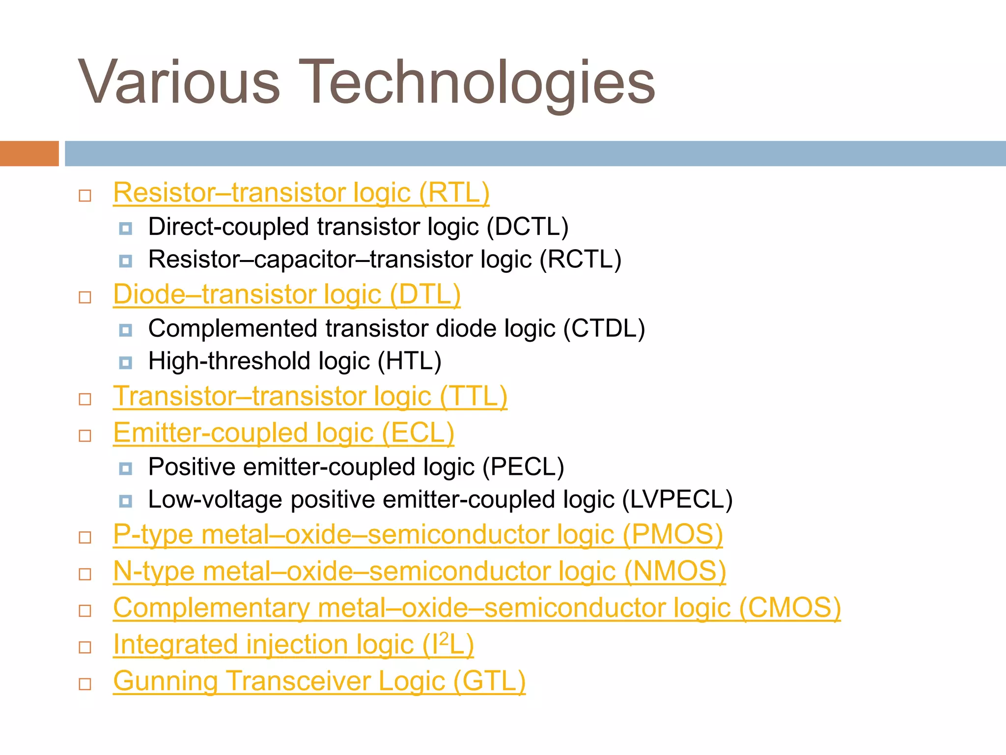
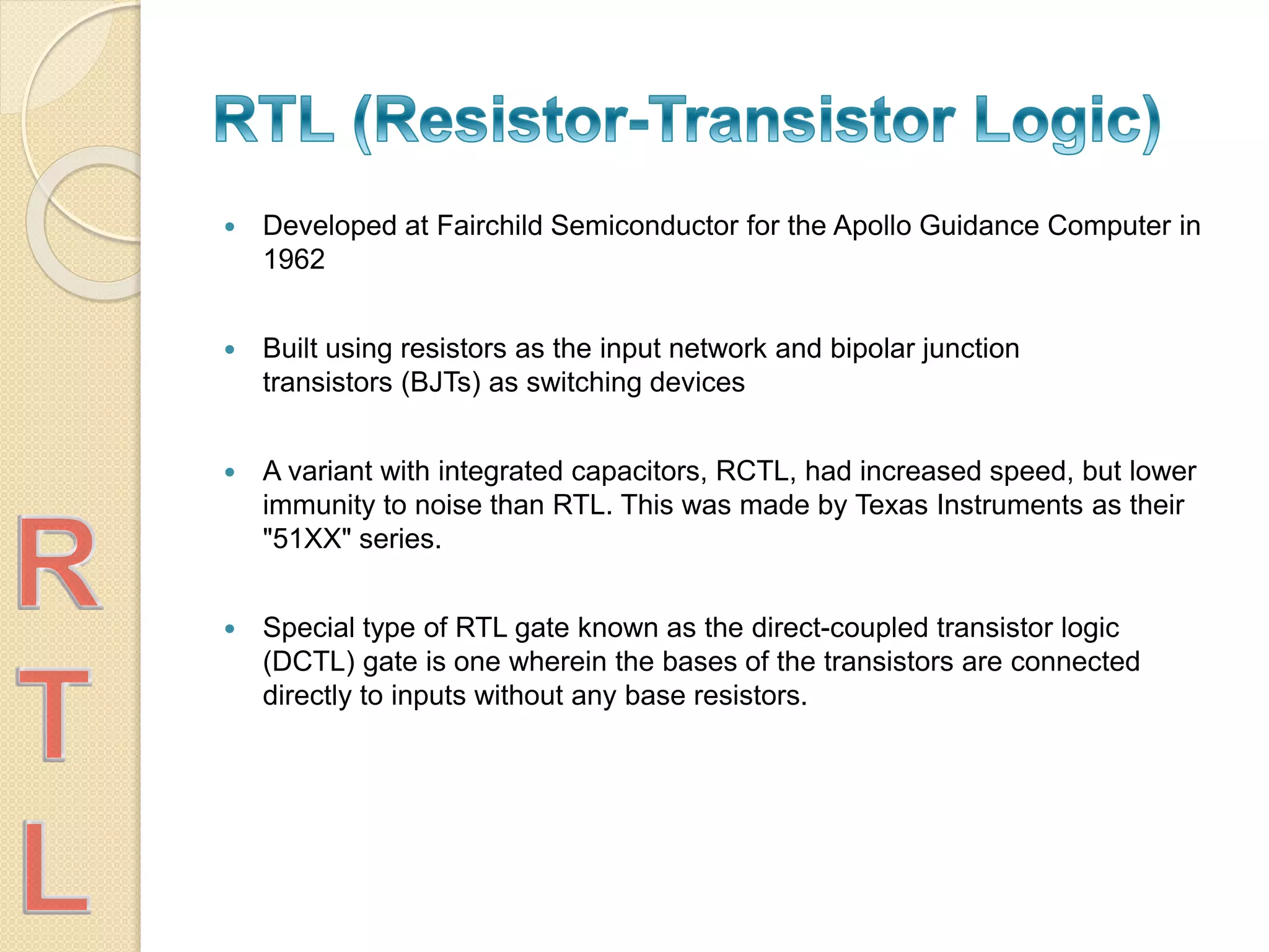
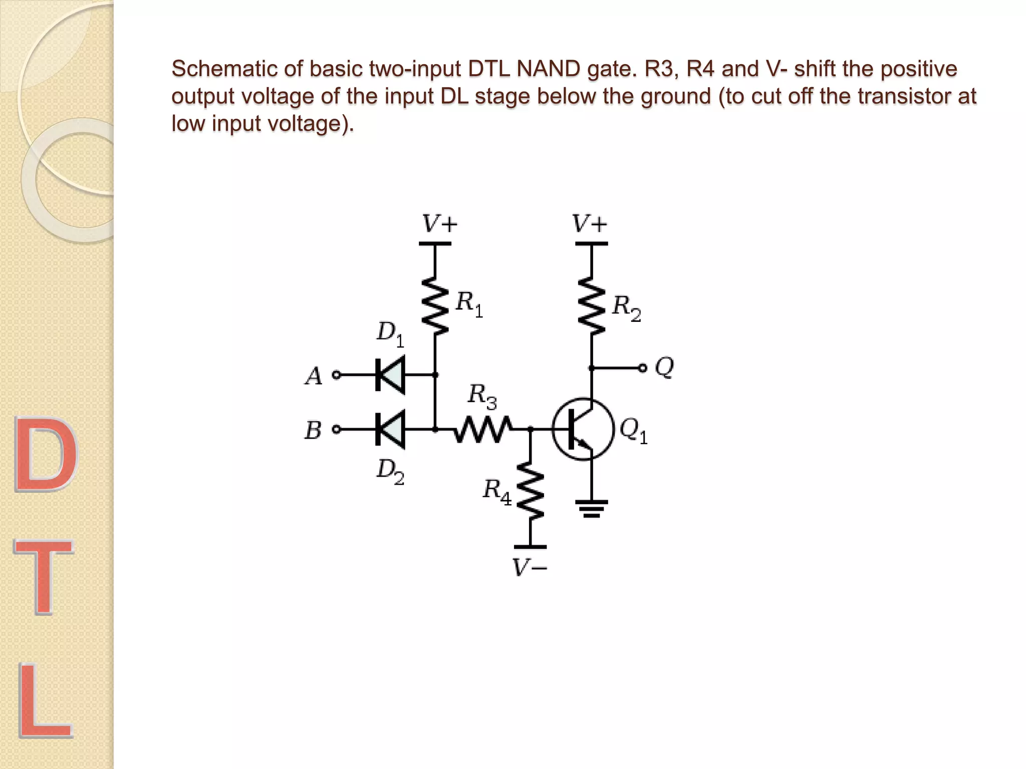
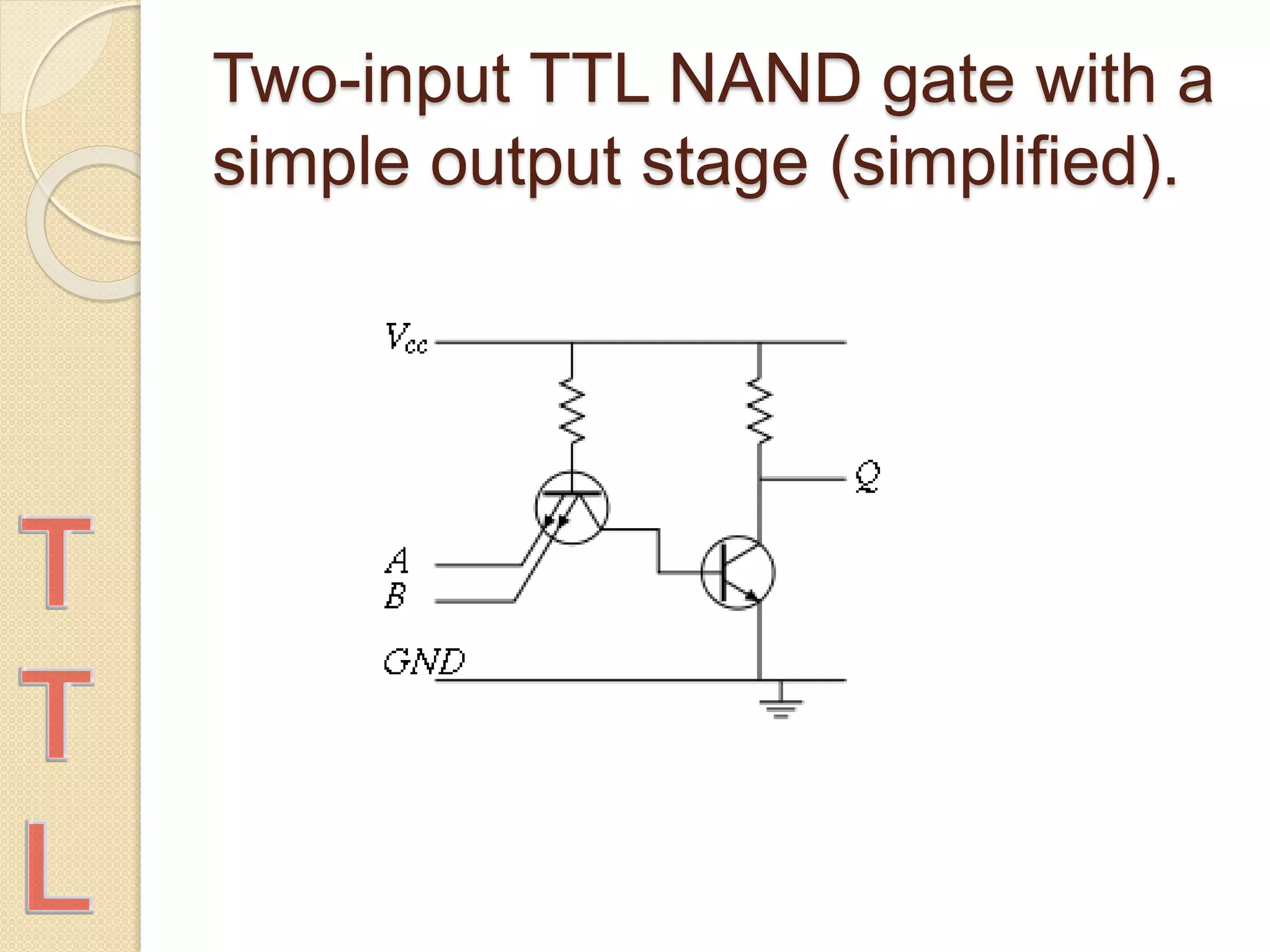
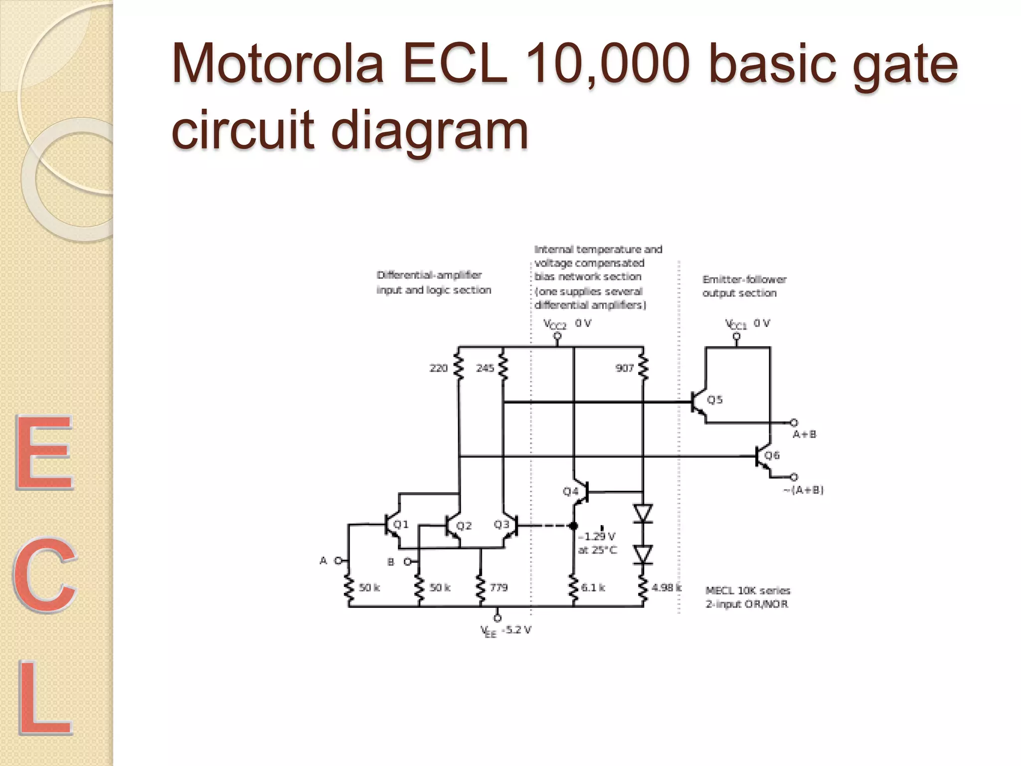
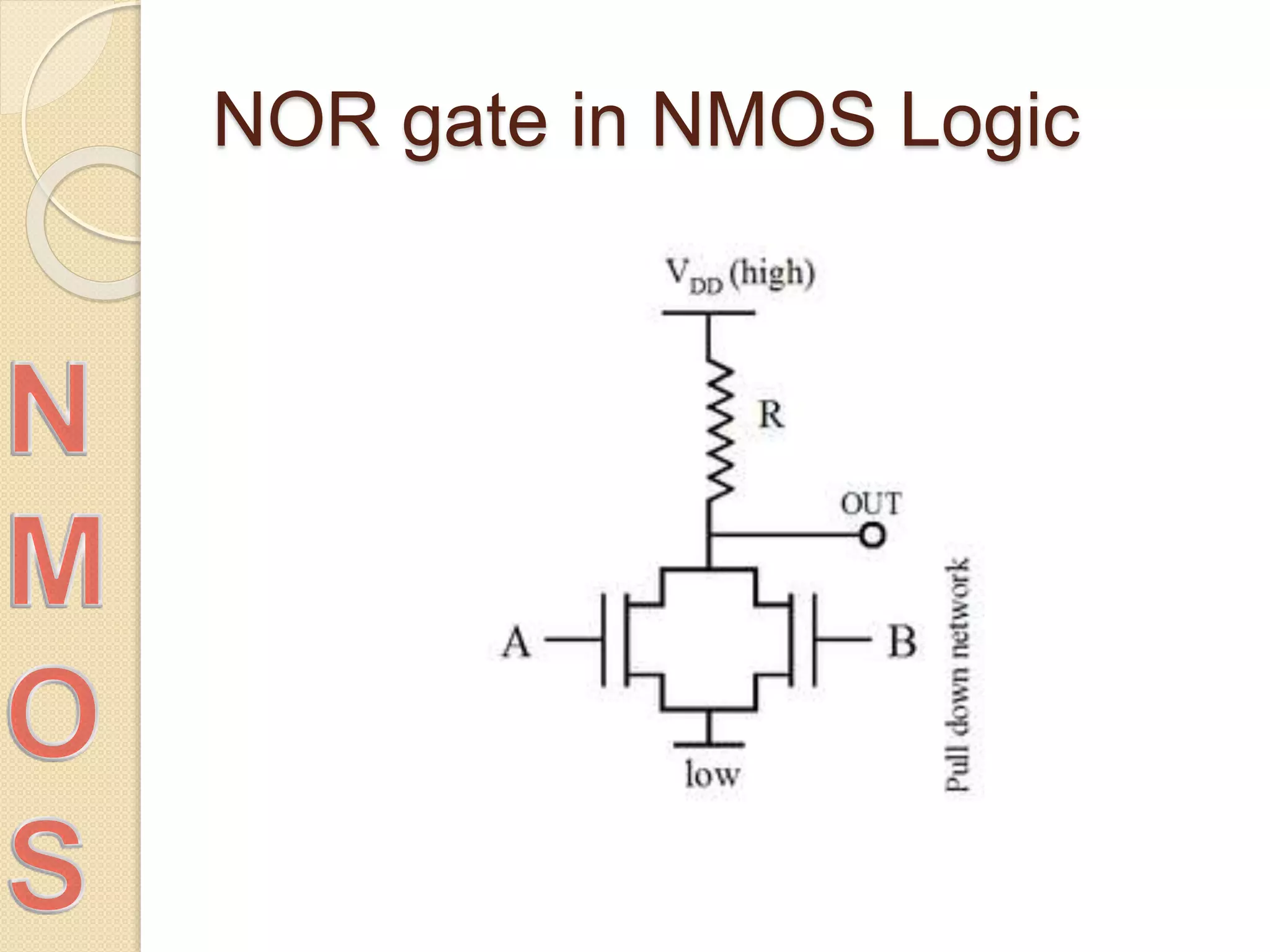
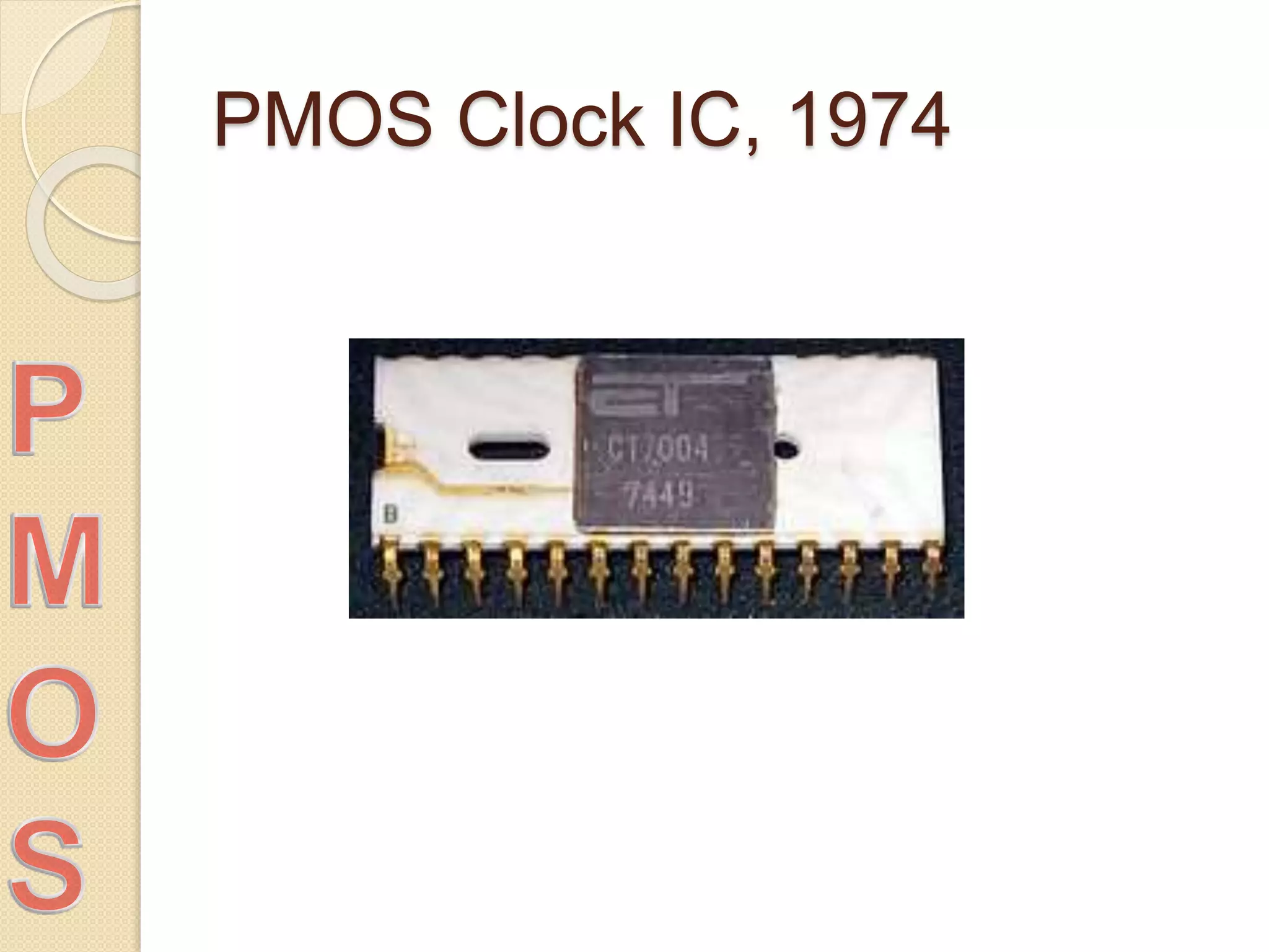
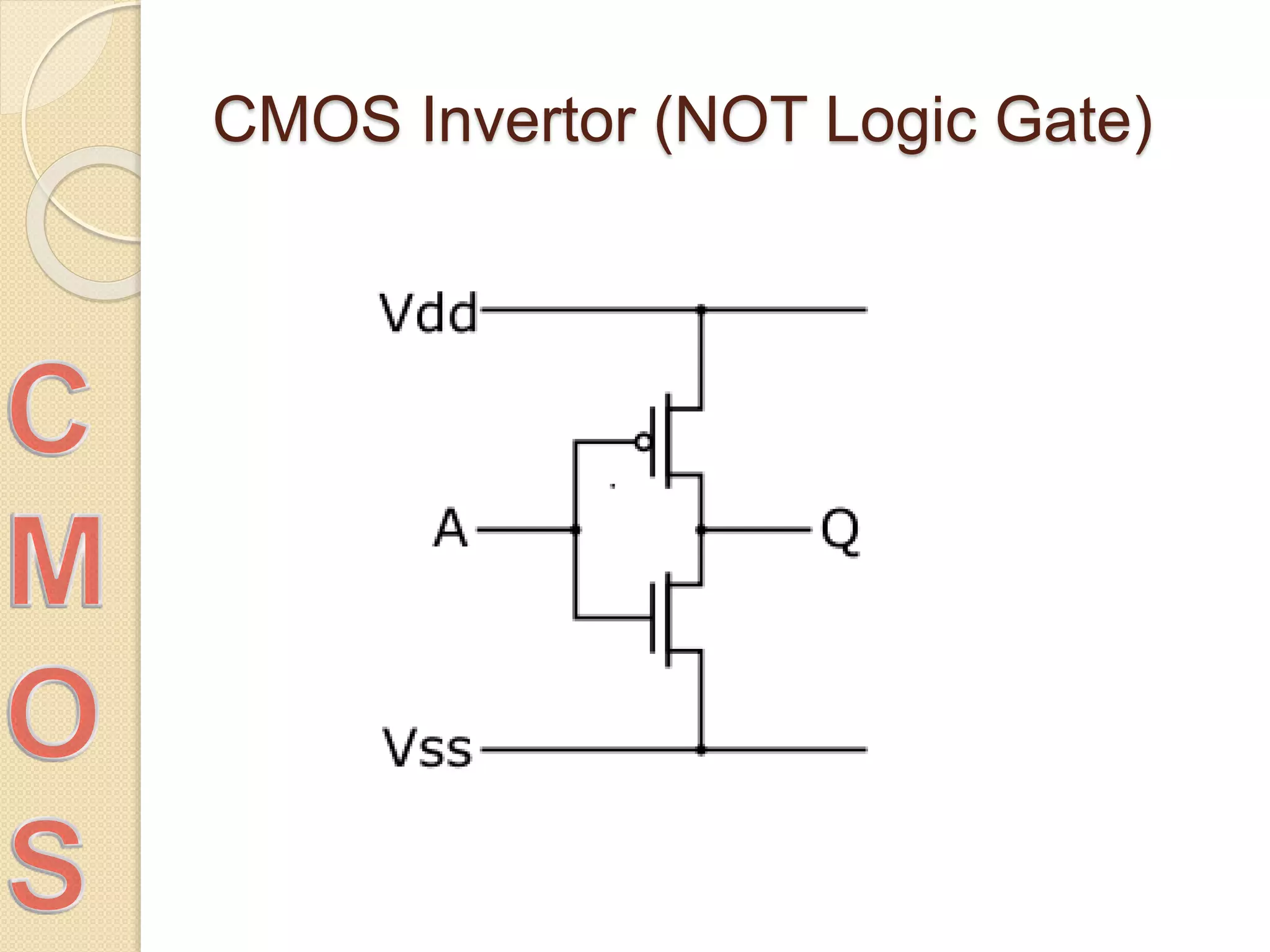
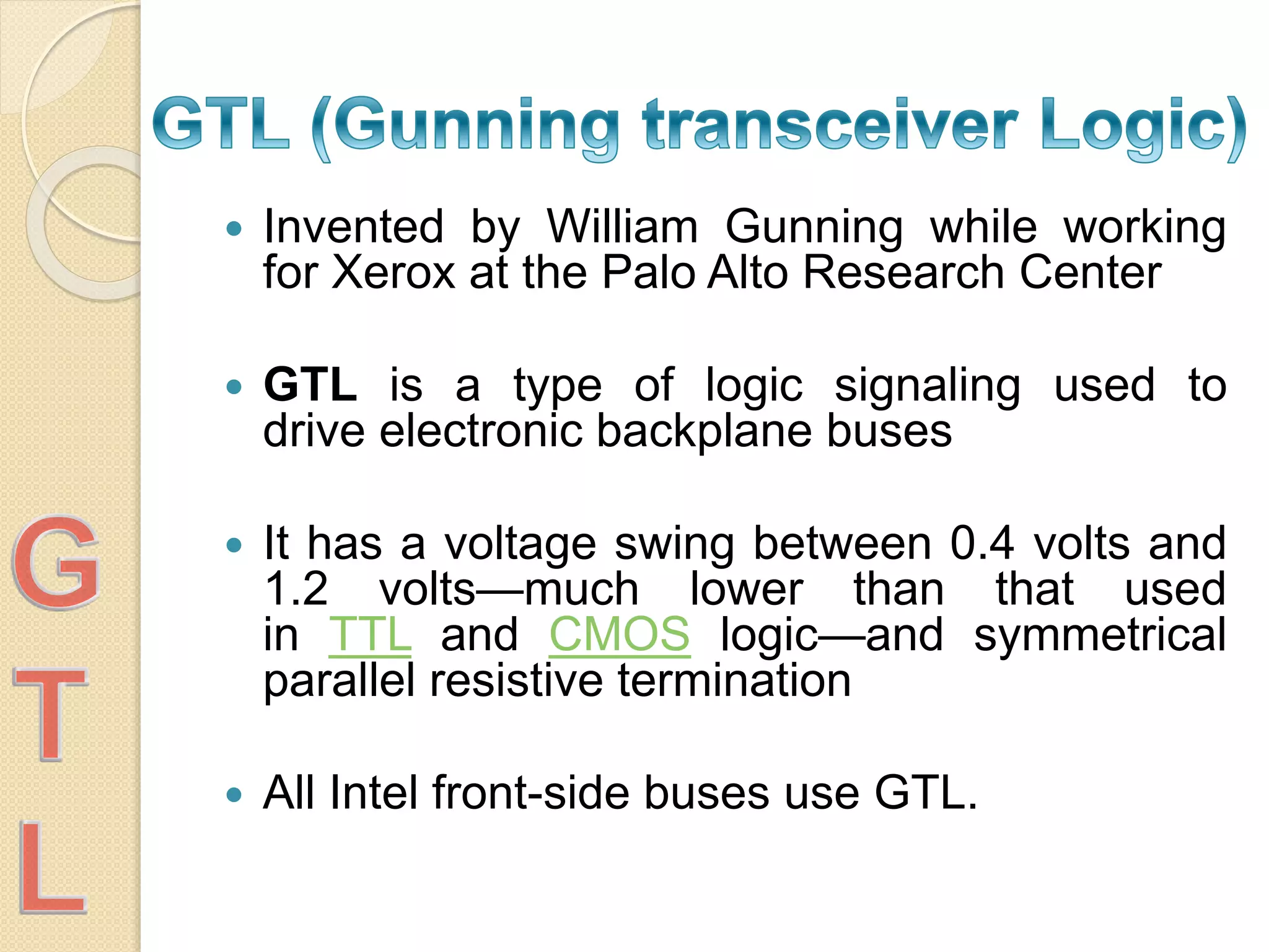
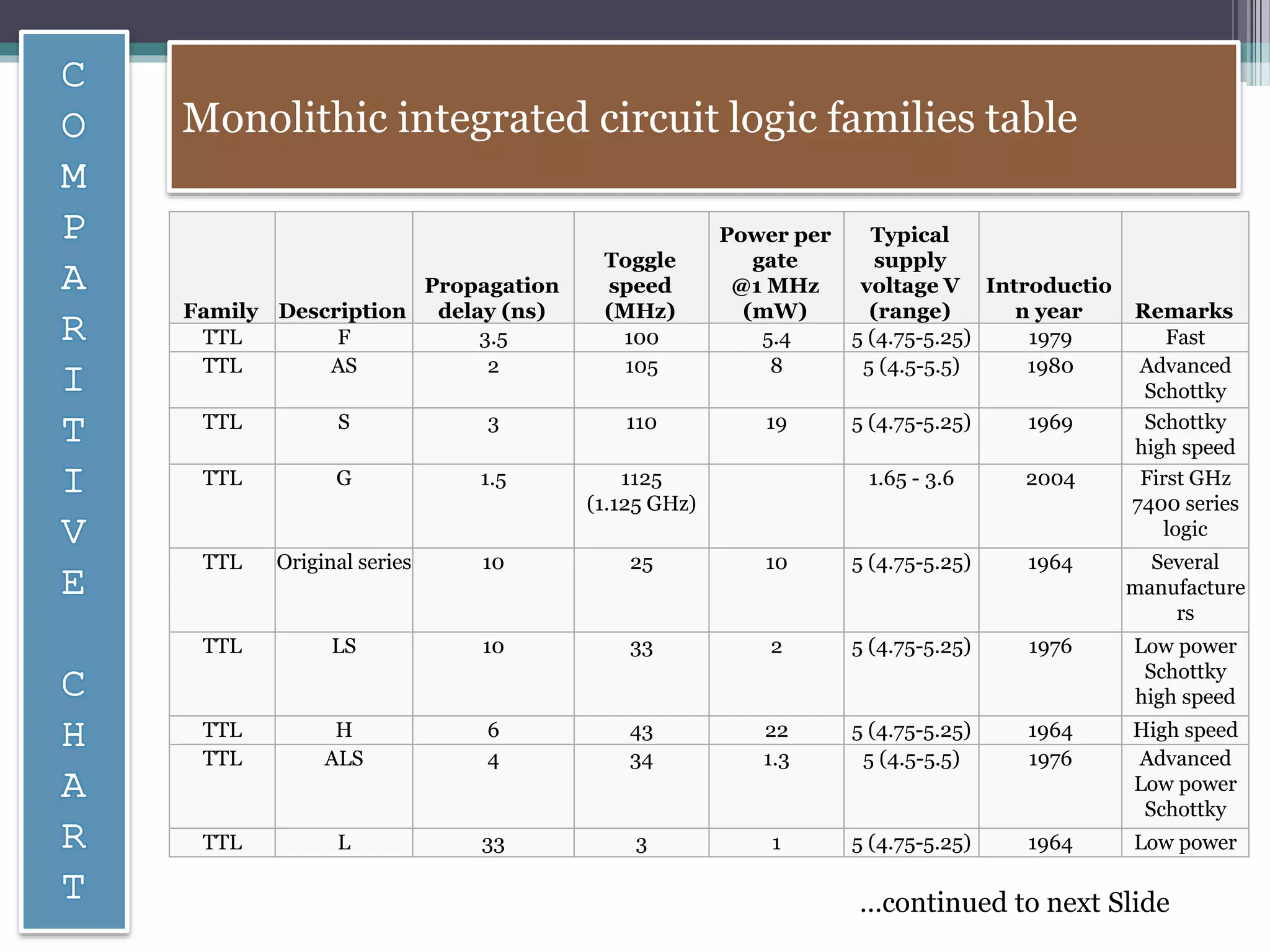
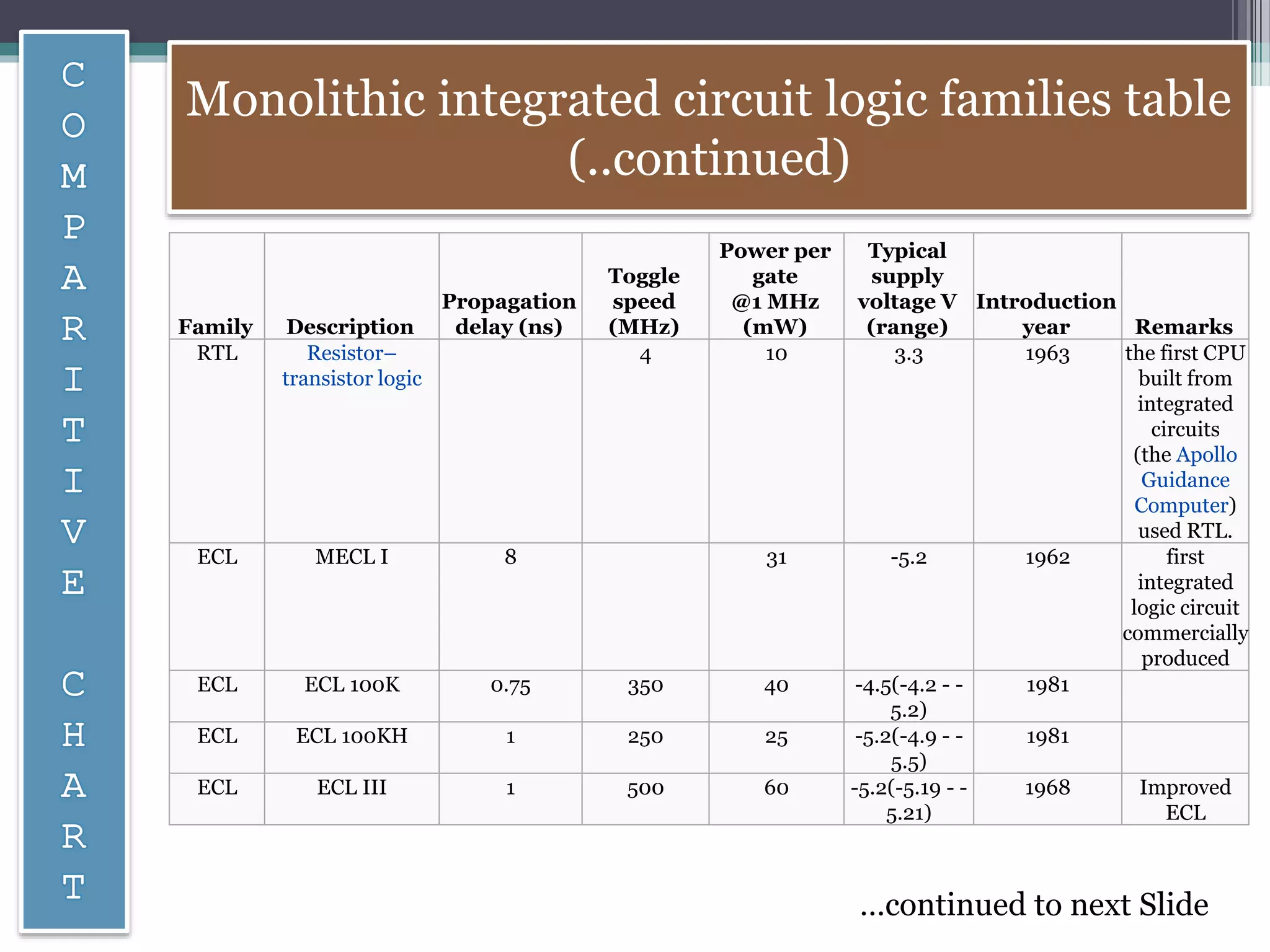
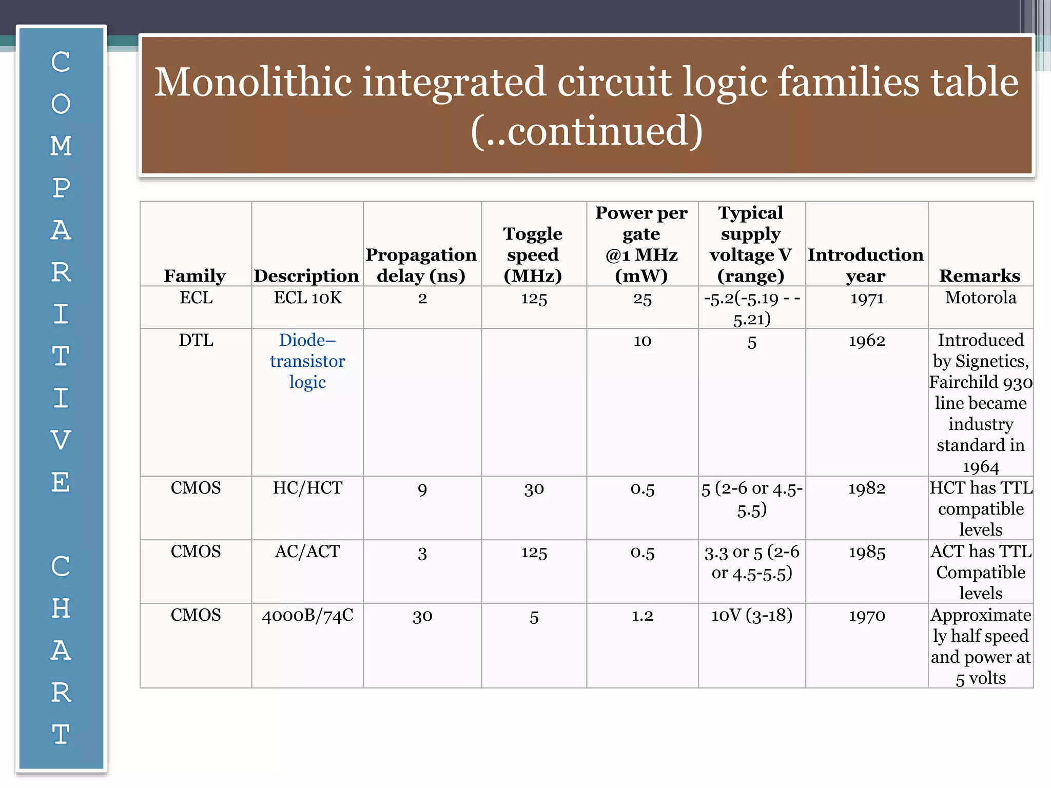
Logic Families
Electronics
Sandeep Kumar Singh
BCA IInd Semester
Introduction
 A logic family of monolithic digital integrated circuit devices is
a group of electronic logic gates constructed using one of
several different designs, usually with compatible logic
levels and power supply characteristics within a family
 A "logic family" may also refer to a set of techniques used to
implement logic within VLSI integrated circuits such as central
processors, memories, or other complex functions.
 Many logic families were produced as individual components,
each containing one or a few related basic logical functions,
which could be used as "building-blocks" to create systems or
as so-called "glue" to interconnect more complex integrated
circuits
Various Technologies
 Resistor–transistor logic (RTL)
 Direct-coupled transistor logic (DCTL)
 Resistor–capacitor–transistor logic (RCTL)
 Diode–transistor logic (DTL)
 Complemented transistor diode logic (CTDL)
 High-threshold logic (HTL)
 Transistor–transistor logic (TTL)
 Emitter-coupled logic (ECL)
 Positive emitter-coupled logic (PECL)
 Low-voltage positive emitter-coupled logic (LVPECL)
 P-type metal–oxide–semiconductor logic (PMOS)
 N-type metal–oxide–semiconductor logic (NMOS)
 Complementary metal–oxide–semiconductor logic (CMOS)
 Integrated injection logic (I2L)
 Gunning Transceiver Logic (GTL)
 Developed at Fairchild Semiconductor for the Apollo Guidance Computer in
1962
 Built using resistors as the input network and bipolar junction
transistors (BJTs) as switching devices
 A variant with integrated capacitors, RCTL, had increased speed, but lower
immunity to noise than RTL. This was made by Texas Instruments as their
"51XX" series.
 Special type of RTL gate known as the direct-coupled transistor logic
(DCTL) gate is one wherein the bases of the transistors are connected
directly to inputs without any base resistors.
Schematic of a one-transistor
RTL NOR gate
• Involved a minimum number of transistors (which was an important
consideration before integrated circuit technology as transistors were
the most expensive component to produce.)
• DCTL gates are more economical and simpler to fabricate onto
integrated circuits than RTL
• The obvious disadvantage of RTL is its high power dissipation when the
transistor is switched on
• Bulkiness
• Low speed
• Limited fan-out
• Poor noise margin
• DCTL gates suffer from a phenomenon known as current hogging.
• DTL was made by Fairchild and Westinghouse
• Technology for designing and fabricating digital circuits wherein logic
gates employ both diodes and transistors
• Diode logic goes back as far as ENIAC and was used in many
early vacuum tube computers
• Logic gating function (e.g., AND) is performed by a diode network and
the amplifying function is performed by a transistor (contrast this
with RTL and TTL)
• The DTL propagation delay is relatively large
Schematic of basic two-input DTL NAND gate. R3, R4 and V- shift the positive
output voltage of the input DL stage below the ground (to cut off the transistor at
low input voltage).
 Offers better noise margins than RTL
 Greater fan-outs than RTL
 The obvious disadvantage of RTL is
its high power dissipation when the
transistor is switched on
 low speed,specially in comparison to
TTL
 Built from bipolar junction transistors (BJT)
and resistors.
 It is called transistor–transistor logic because
both the logic gating function (e.g., AND) and
the amplifying function are performed by
transistors
 TTL is notable for being a widespread
integrated circuit (IC) family used in many
applications such as computers, industrial
controls, test equipment and instrumentation,
consumer electronics, synthesizers).
Two-input TTL NAND gate with a
simple output stage (simplified).
 TTL is less sensitive to damage
from electrostatic discharge than early CMOS
devices
 Compared to Contemporary ECL circuits, TTL
uses less power and has easier design rules.
 TTL is particularly well suited to bipolar
integrated circuits because additional inputs
to a gate merely required additional emitters
on a shared base region of the input
transistor
 TTL devices consume substantially more
power than equivalent CMOS devices at rest,
but power consumption does not increase
with clock speed as rapidly as for CMOS
devices
 Substantially slower than ECL
 Due to the output structure of TTL devices,
the output impedance is asymmetrical
between the high and low state, making them
unsuitable for driving transmission lines
 Based on the use of a multi-input differential amplifier to
amplify and combine the digital signals, and emitter
followers to adjust the dc voltage levels
 Achieves high speed by using an
overdriven BJT differential amplifier with single-ended
input whose emitter current is limited to avoid the
slow saturation region of transistor operation
 As the current is steered between two legs of an
emitter-coupled pair, ECL is sometimes called current-
steering logic (CSL),current-mode
logic (CML) or current-switch emitter-follower (CSEF)
logic
Motorola ECL 10,000 basic gate
circuit diagram
 Changes state quickly
 Low gate delay
 High Fan out
 Constant current draw of the differential
amplifiers minimizes delays and glitches
due to supply-line inductance and
capacitance
 Each gate continuously draws current,
which means it requires (and
dissipates) significantly more power
than those of other logic families,
especially when quiescent.
 ECL suffers from small noise margins,
which can be troublesome
 Uses n-type metal-oxide-semiconductor field
effect transistors (MOSFETs) to implement logic
gates and other digital circuits
 NMOS transistors have four modes of operation:
cut-off (or sub-threshold), triode, saturation
(sometimes called active), and velocity saturation
 Better (and the most common) way to make the
gates faster is to use depletion-mode transistors
instead of enhancement-mode transistors as
loads. This is called depletion-load NMOS logic
NOR gate in NMOS Logic
 Much faster than comparable PMOS
and CMOS circuits
 Easier to manufacture NMOS than
CMOS
 The major problem with NMOS (and
most other logic families) is that a DC
current must flow through a logic gate
even when the output is in a steady
state (low in the case of NMOS)
 Slow to transition from low to high
 The asymmetric input logic levels make
NMOS circuits somewhat susceptible to
noise
 Uses p-type metal oxide semiconductor
field effect transistors (MOSFETs) to
implement logic gates and other digital
circuits
 PMOS transistors have four modes of
operation: cut-off (or subthreshold),
triode, saturation (sometimes called
active), and velocity saturation
PMOS Clock IC, 1974
 PMOS logic is easy to design and
manufacture
 DC current flows through a PMOS logic gate when the
PUN(pull up network) is active, that is whenever the
output is high. This leads to static power dissipation
even when the circuit sits idle
 PMOS circuits are slow to transition from high to low
 Using a resistor of lower value will speed up the
process but also increases static power dissipation
 The asymmetric input logic levels make PMOS circuits
susceptible to noise
 CMOS circuits were invented by Frank Wanlass of Fairchild
Semiconductor in 1963, although the first CMOS I.C.'s were
not produced until 1968, this time at RCA
 Technology for designing and fabricating integrated circuits
that employ logic using both n- and p-channel MOSFET's
 CMOS is the other major technology utilized in manufacturing
digital IC's aside from TTL
 CMOS technology is also used for several analog circuits
such as image sensors(CMOS sensor), data converters, and
highly integrated transceivers for many types of
communication
CMOS Invertor (NOT Logic Gate)
 High noise immunity
 Low static power consumption
 Do not produce as much waste heat as other
forms of logic
 Allows a high density of logic functions on a
chip. It was primarily for this reason that
CMOS became the most used technology to
be implemented in VLSI chips
 CMOS circuits are quite vulnerable
to ESD damage. Because of this
issue, modern CMOS IC's are now
equipped with on-chip ESD protection
circuits, which reduce (but not totally
eliminate) risks of ESD damage
 Class of digital circuits built with multiple collector
bipolar junction transistors
 When introduced it had speed comparable to TTL yet
was almost as low power as CMOS, making it ideal for
use in VLSI (and larger) integrated circuits
 IIL is relatively simple to construct on an integrated
circuit
 Logic voltage levels are very close (High: 0.7V, Low:
0.2V), I2L has high noise immunity because it operates
by current instead of voltage. Sometimes also known as
Merged Transistor Logic
Integrated Injection Logic Circuit
 Invented by William Gunning while working
for Xerox at the Palo Alto Research Center
 GTL is a type of logic signaling used to
drive electronic backplane buses
 It has a voltage swing between 0.4 volts and
1.2 volts—much lower than that used
in TTL and CMOS logic—and symmetrical
parallel resistive termination
 All Intel front-side buses use GTL.
Monolithic integrated circuit logic families table
Family Description
Propagation
delay (ns)
Toggle
speed
(MHz)
Power per
gate
@1 MHz
(mW)
Typical
supply
voltage V
(range)
Introductio
n year Remarks
TTL F 3.5 100 5.4 5 (4.75-5.25) 1979 Fast
TTL AS 2 105 8 5 (4.5-5.5) 1980 Advanced
Schottky
TTL S 3 110 19 5 (4.75-5.25) 1969 Schottky
high speed
TTL G 1.5 1125
(1.125 GHz)
1.65 - 3.6 2004 First GHz
7400 series
logic
TTL Original series 10 25 10 5 (4.75-5.25) 1964 Several
manufacture
rs
TTL LS 10 33 2 5 (4.75-5.25) 1976 Low power
Schottky
high speed
TTL H 6 43 22 5 (4.75-5.25) 1964 High speed
TTL ALS 4 34 1.3 5 (4.5-5.5) 1976 Advanced
Low power
Schottky
TTL L 33 3 1 5 (4.75-5.25) 1964 Low power
…continued to next Slide
Family Description
Propagation
delay (ns)
Toggle
speed
(MHz)
Power per
gate
@1 MHz
(mW)
Typical
supply
voltage V
(range)
Introduction
year Remarks
RTL Resistor–
transistor logic
4 10 3.3 1963 the first CPU
built from
integrated
circuits
(the Apollo
Guidance
Computer)
used RTL.
ECL MECL I 8 31 -5.2 1962 first
integrated
logic circuit
commercially
produced
ECL ECL 100K 0.75 350 40 -4.5(-4.2 - -
5.2)
1981
ECL ECL 100KH 1 250 25 -5.2(-4.9 - -
5.5)
1981
ECL ECL III 1 500 60 -5.2(-5.19 - -
5.21)
1968 Improved
ECL
Monolithic integrated circuit logic families table
(..continued)
…continued to next Slide
Family Description
Propagation
delay (ns)
Toggle
speed
(MHz)
Power per
gate
@1 MHz
(mW)
Typical
supply
voltage V
(range)
Introduction
year Remarks
ECL ECL 10K 2 125 25 -5.2(-5.19 - -
5.21)
1971 Motorola
DTL Diode–
transistor
logic
10 5 1962 Introduced
by Signetics,
Fairchild 930
line became
industry
standard in
1964
CMOS HC/HCT 9 30 0.5 5 (2-6 or 4.5-
5.5)
1982 HCT has TTL
compatible
levels
CMOS AC/ACT 3 125 0.5 3.3 or 5 (2-6
or 4.5-5.5)
1985 ACT has TTL
Compatible
levels
CMOS 4000B/74C 30 5 1.2 10V (3-18) 1970 Approximate
ly half speed
and power at
5 volts
Monolithic integrated circuit logic families table
(..continued)
 Fan out - fan-out of a gate is the ability of its output to drive several
other gates. The more gates it can drive, the higher is its fan-out
 Gate Delay - Gate delay is the delay offered by a gate for the signal
appearing at its input, before it reaches the gate output
 Noise Margin - Undesirable voltage variations that are superimposed on
normal operating voltage levels are called noise. All gates are designed to
tolerate a certain amount of noise on their input and output ports. The
maximum noise voltage level that is tolerated by a gate is called noise
margin
 Propagation Delay - The time between the logic transition on an input
and the corresponding logic transition on the output of the logic gate
Basic Concepts
 Wikipedia, the free encyclopedia
 www.play-hookey.com/digital/electronics
 http://www.asic-world.com/digital/seq.html
 www.siliconfareast.com
Logic families

Logic families

  • 1.
  • 2.
    Introduction  A logicfamily of monolithic digital integrated circuit devices is a group of electronic logic gates constructed using one of several different designs, usually with compatible logic levels and power supply characteristics within a family  A "logic family" may also refer to a set of techniques used to implement logic within VLSI integrated circuits such as central processors, memories, or other complex functions.  Many logic families were produced as individual components, each containing one or a few related basic logical functions, which could be used as "building-blocks" to create systems or as so-called "glue" to interconnect more complex integrated circuits
  • 3.
    Various Technologies  Resistor–transistorlogic (RTL)  Direct-coupled transistor logic (DCTL)  Resistor–capacitor–transistor logic (RCTL)  Diode–transistor logic (DTL)  Complemented transistor diode logic (CTDL)  High-threshold logic (HTL)  Transistor–transistor logic (TTL)  Emitter-coupled logic (ECL)  Positive emitter-coupled logic (PECL)  Low-voltage positive emitter-coupled logic (LVPECL)  P-type metal–oxide–semiconductor logic (PMOS)  N-type metal–oxide–semiconductor logic (NMOS)  Complementary metal–oxide–semiconductor logic (CMOS)  Integrated injection logic (I2L)  Gunning Transceiver Logic (GTL)
  • 4.
     Developed atFairchild Semiconductor for the Apollo Guidance Computer in 1962  Built using resistors as the input network and bipolar junction transistors (BJTs) as switching devices  A variant with integrated capacitors, RCTL, had increased speed, but lower immunity to noise than RTL. This was made by Texas Instruments as their "51XX" series.  Special type of RTL gate known as the direct-coupled transistor logic (DCTL) gate is one wherein the bases of the transistors are connected directly to inputs without any base resistors.
  • 5.
    Schematic of aone-transistor RTL NOR gate
  • 6.
    • Involved aminimum number of transistors (which was an important consideration before integrated circuit technology as transistors were the most expensive component to produce.) • DCTL gates are more economical and simpler to fabricate onto integrated circuits than RTL
  • 7.
    • The obviousdisadvantage of RTL is its high power dissipation when the transistor is switched on • Bulkiness • Low speed • Limited fan-out • Poor noise margin • DCTL gates suffer from a phenomenon known as current hogging.
  • 8.
    • DTL wasmade by Fairchild and Westinghouse • Technology for designing and fabricating digital circuits wherein logic gates employ both diodes and transistors • Diode logic goes back as far as ENIAC and was used in many early vacuum tube computers • Logic gating function (e.g., AND) is performed by a diode network and the amplifying function is performed by a transistor (contrast this with RTL and TTL) • The DTL propagation delay is relatively large
  • 9.
    Schematic of basictwo-input DTL NAND gate. R3, R4 and V- shift the positive output voltage of the input DL stage below the ground (to cut off the transistor at low input voltage).
  • 10.
     Offers betternoise margins than RTL  Greater fan-outs than RTL
  • 11.
     The obviousdisadvantage of RTL is its high power dissipation when the transistor is switched on  low speed,specially in comparison to TTL
  • 12.
     Built frombipolar junction transistors (BJT) and resistors.  It is called transistor–transistor logic because both the logic gating function (e.g., AND) and the amplifying function are performed by transistors  TTL is notable for being a widespread integrated circuit (IC) family used in many applications such as computers, industrial controls, test equipment and instrumentation, consumer electronics, synthesizers).
  • 13.
    Two-input TTL NANDgate with a simple output stage (simplified).
  • 14.
     TTL isless sensitive to damage from electrostatic discharge than early CMOS devices  Compared to Contemporary ECL circuits, TTL uses less power and has easier design rules.  TTL is particularly well suited to bipolar integrated circuits because additional inputs to a gate merely required additional emitters on a shared base region of the input transistor
  • 15.
     TTL devicesconsume substantially more power than equivalent CMOS devices at rest, but power consumption does not increase with clock speed as rapidly as for CMOS devices  Substantially slower than ECL  Due to the output structure of TTL devices, the output impedance is asymmetrical between the high and low state, making them unsuitable for driving transmission lines
  • 16.
     Based onthe use of a multi-input differential amplifier to amplify and combine the digital signals, and emitter followers to adjust the dc voltage levels  Achieves high speed by using an overdriven BJT differential amplifier with single-ended input whose emitter current is limited to avoid the slow saturation region of transistor operation  As the current is steered between two legs of an emitter-coupled pair, ECL is sometimes called current- steering logic (CSL),current-mode logic (CML) or current-switch emitter-follower (CSEF) logic
  • 17.
    Motorola ECL 10,000basic gate circuit diagram
  • 18.
     Changes statequickly  Low gate delay  High Fan out  Constant current draw of the differential amplifiers minimizes delays and glitches due to supply-line inductance and capacitance
  • 19.
     Each gatecontinuously draws current, which means it requires (and dissipates) significantly more power than those of other logic families, especially when quiescent.  ECL suffers from small noise margins, which can be troublesome
  • 20.
     Uses n-typemetal-oxide-semiconductor field effect transistors (MOSFETs) to implement logic gates and other digital circuits  NMOS transistors have four modes of operation: cut-off (or sub-threshold), triode, saturation (sometimes called active), and velocity saturation  Better (and the most common) way to make the gates faster is to use depletion-mode transistors instead of enhancement-mode transistors as loads. This is called depletion-load NMOS logic
  • 21.
    NOR gate inNMOS Logic
  • 22.
     Much fasterthan comparable PMOS and CMOS circuits  Easier to manufacture NMOS than CMOS
  • 23.
     The majorproblem with NMOS (and most other logic families) is that a DC current must flow through a logic gate even when the output is in a steady state (low in the case of NMOS)  Slow to transition from low to high  The asymmetric input logic levels make NMOS circuits somewhat susceptible to noise
  • 24.
     Uses p-typemetal oxide semiconductor field effect transistors (MOSFETs) to implement logic gates and other digital circuits  PMOS transistors have four modes of operation: cut-off (or subthreshold), triode, saturation (sometimes called active), and velocity saturation
  • 25.
  • 26.
     PMOS logicis easy to design and manufacture
  • 27.
     DC currentflows through a PMOS logic gate when the PUN(pull up network) is active, that is whenever the output is high. This leads to static power dissipation even when the circuit sits idle  PMOS circuits are slow to transition from high to low  Using a resistor of lower value will speed up the process but also increases static power dissipation  The asymmetric input logic levels make PMOS circuits susceptible to noise
  • 28.
     CMOS circuitswere invented by Frank Wanlass of Fairchild Semiconductor in 1963, although the first CMOS I.C.'s were not produced until 1968, this time at RCA  Technology for designing and fabricating integrated circuits that employ logic using both n- and p-channel MOSFET's  CMOS is the other major technology utilized in manufacturing digital IC's aside from TTL  CMOS technology is also used for several analog circuits such as image sensors(CMOS sensor), data converters, and highly integrated transceivers for many types of communication
  • 29.
    CMOS Invertor (NOTLogic Gate)
  • 30.
     High noiseimmunity  Low static power consumption  Do not produce as much waste heat as other forms of logic  Allows a high density of logic functions on a chip. It was primarily for this reason that CMOS became the most used technology to be implemented in VLSI chips
  • 31.
     CMOS circuitsare quite vulnerable to ESD damage. Because of this issue, modern CMOS IC's are now equipped with on-chip ESD protection circuits, which reduce (but not totally eliminate) risks of ESD damage
  • 32.
     Class ofdigital circuits built with multiple collector bipolar junction transistors  When introduced it had speed comparable to TTL yet was almost as low power as CMOS, making it ideal for use in VLSI (and larger) integrated circuits  IIL is relatively simple to construct on an integrated circuit  Logic voltage levels are very close (High: 0.7V, Low: 0.2V), I2L has high noise immunity because it operates by current instead of voltage. Sometimes also known as Merged Transistor Logic
  • 33.
  • 34.
     Invented byWilliam Gunning while working for Xerox at the Palo Alto Research Center  GTL is a type of logic signaling used to drive electronic backplane buses  It has a voltage swing between 0.4 volts and 1.2 volts—much lower than that used in TTL and CMOS logic—and symmetrical parallel resistive termination  All Intel front-side buses use GTL.
  • 35.
    Monolithic integrated circuitlogic families table Family Description Propagation delay (ns) Toggle speed (MHz) Power per gate @1 MHz (mW) Typical supply voltage V (range) Introductio n year Remarks TTL F 3.5 100 5.4 5 (4.75-5.25) 1979 Fast TTL AS 2 105 8 5 (4.5-5.5) 1980 Advanced Schottky TTL S 3 110 19 5 (4.75-5.25) 1969 Schottky high speed TTL G 1.5 1125 (1.125 GHz) 1.65 - 3.6 2004 First GHz 7400 series logic TTL Original series 10 25 10 5 (4.75-5.25) 1964 Several manufacture rs TTL LS 10 33 2 5 (4.75-5.25) 1976 Low power Schottky high speed TTL H 6 43 22 5 (4.75-5.25) 1964 High speed TTL ALS 4 34 1.3 5 (4.5-5.5) 1976 Advanced Low power Schottky TTL L 33 3 1 5 (4.75-5.25) 1964 Low power …continued to next Slide
  • 36.
    Family Description Propagation delay (ns) Toggle speed (MHz) Powerper gate @1 MHz (mW) Typical supply voltage V (range) Introduction year Remarks RTL Resistor– transistor logic 4 10 3.3 1963 the first CPU built from integrated circuits (the Apollo Guidance Computer) used RTL. ECL MECL I 8 31 -5.2 1962 first integrated logic circuit commercially produced ECL ECL 100K 0.75 350 40 -4.5(-4.2 - - 5.2) 1981 ECL ECL 100KH 1 250 25 -5.2(-4.9 - - 5.5) 1981 ECL ECL III 1 500 60 -5.2(-5.19 - - 5.21) 1968 Improved ECL Monolithic integrated circuit logic families table (..continued) …continued to next Slide
  • 37.
    Family Description Propagation delay (ns) Toggle speed (MHz) Powerper gate @1 MHz (mW) Typical supply voltage V (range) Introduction year Remarks ECL ECL 10K 2 125 25 -5.2(-5.19 - - 5.21) 1971 Motorola DTL Diode– transistor logic 10 5 1962 Introduced by Signetics, Fairchild 930 line became industry standard in 1964 CMOS HC/HCT 9 30 0.5 5 (2-6 or 4.5- 5.5) 1982 HCT has TTL compatible levels CMOS AC/ACT 3 125 0.5 3.3 or 5 (2-6 or 4.5-5.5) 1985 ACT has TTL Compatible levels CMOS 4000B/74C 30 5 1.2 10V (3-18) 1970 Approximate ly half speed and power at 5 volts Monolithic integrated circuit logic families table (..continued)
  • 38.
     Fan out- fan-out of a gate is the ability of its output to drive several other gates. The more gates it can drive, the higher is its fan-out  Gate Delay - Gate delay is the delay offered by a gate for the signal appearing at its input, before it reaches the gate output  Noise Margin - Undesirable voltage variations that are superimposed on normal operating voltage levels are called noise. All gates are designed to tolerate a certain amount of noise on their input and output ports. The maximum noise voltage level that is tolerated by a gate is called noise margin  Propagation Delay - The time between the logic transition on an input and the corresponding logic transition on the output of the logic gate Basic Concepts
  • 39.
     Wikipedia, thefree encyclopedia  www.play-hookey.com/digital/electronics  http://www.asic-world.com/digital/seq.html  www.siliconfareast.com