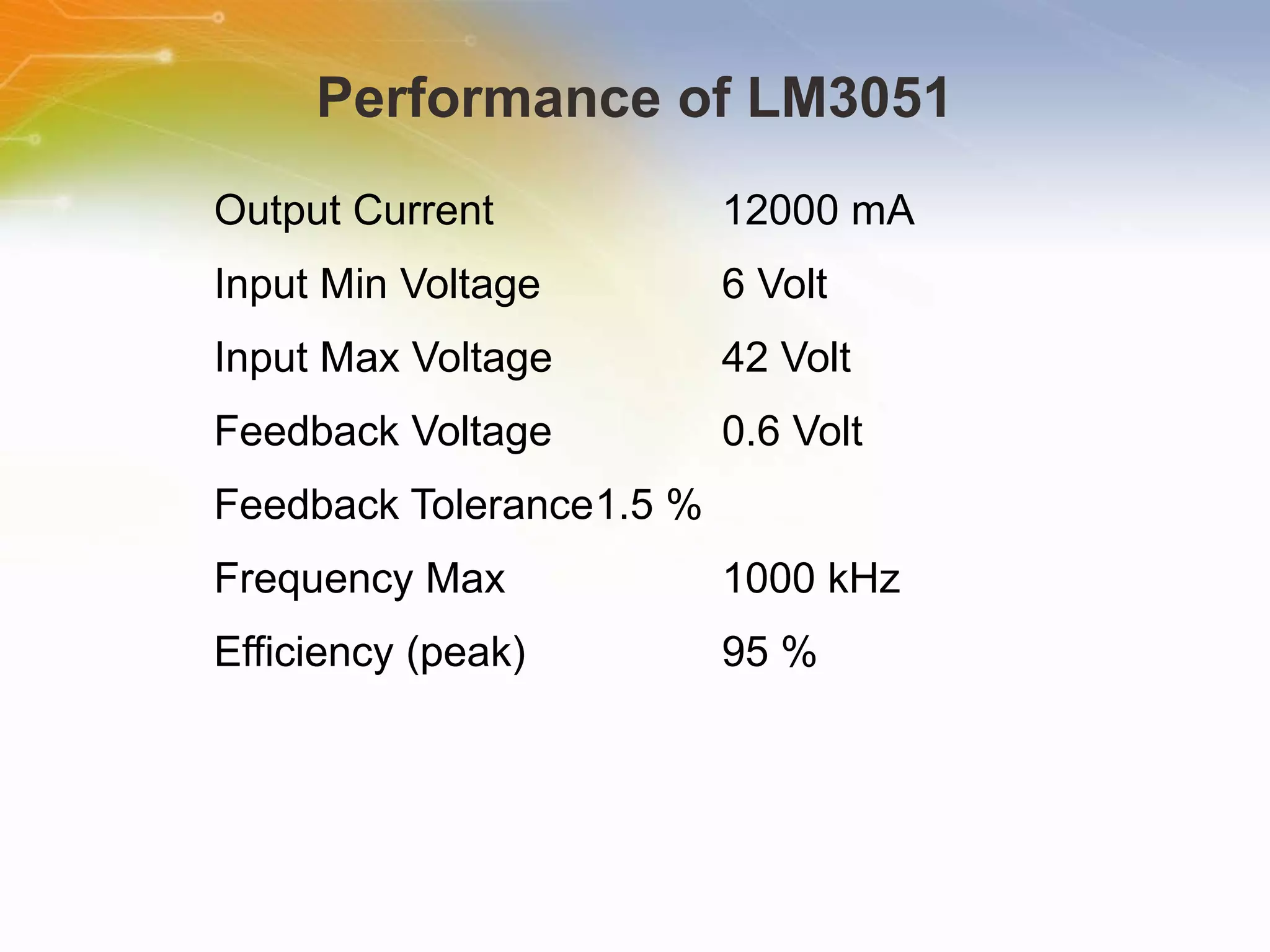
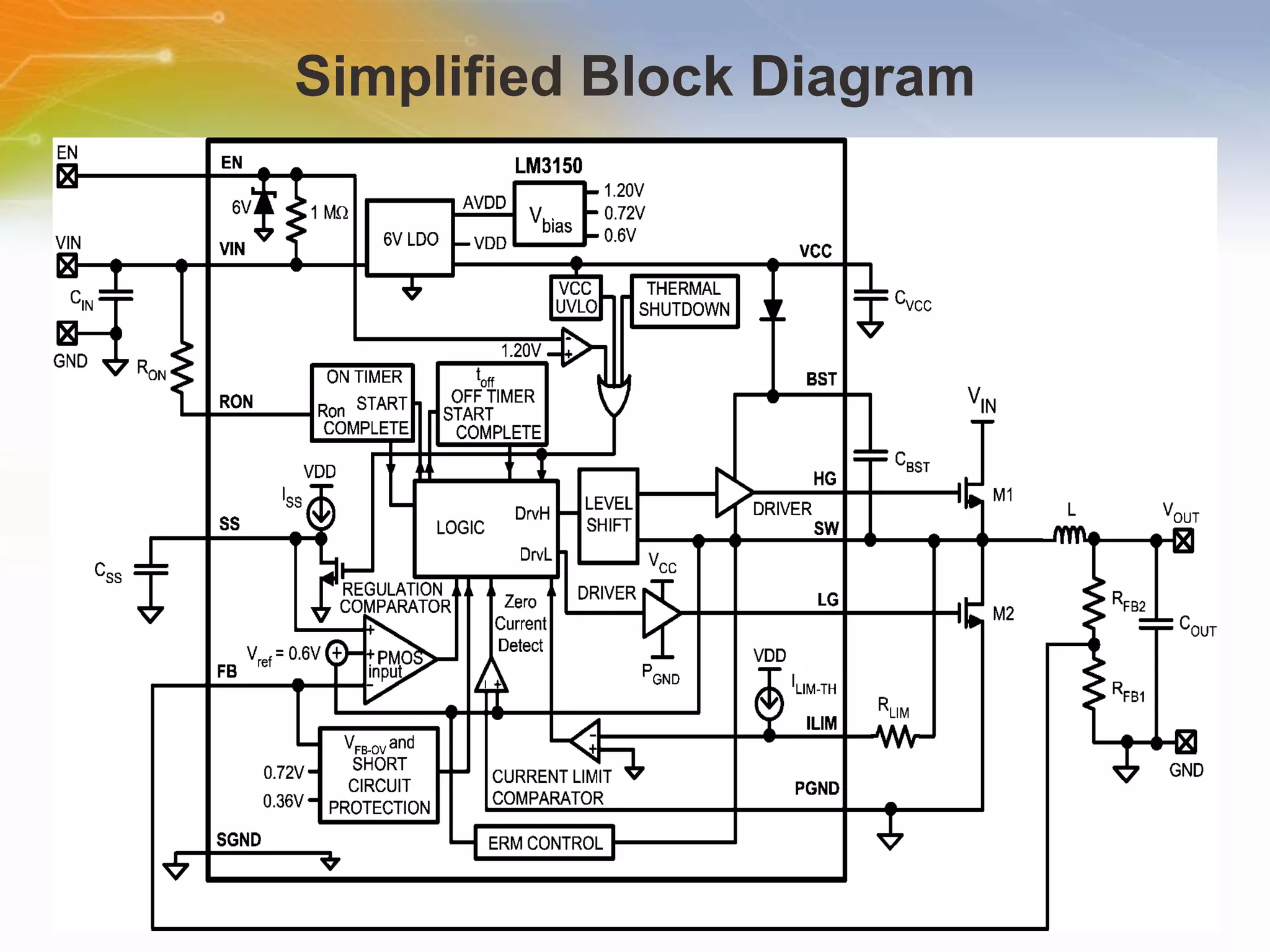
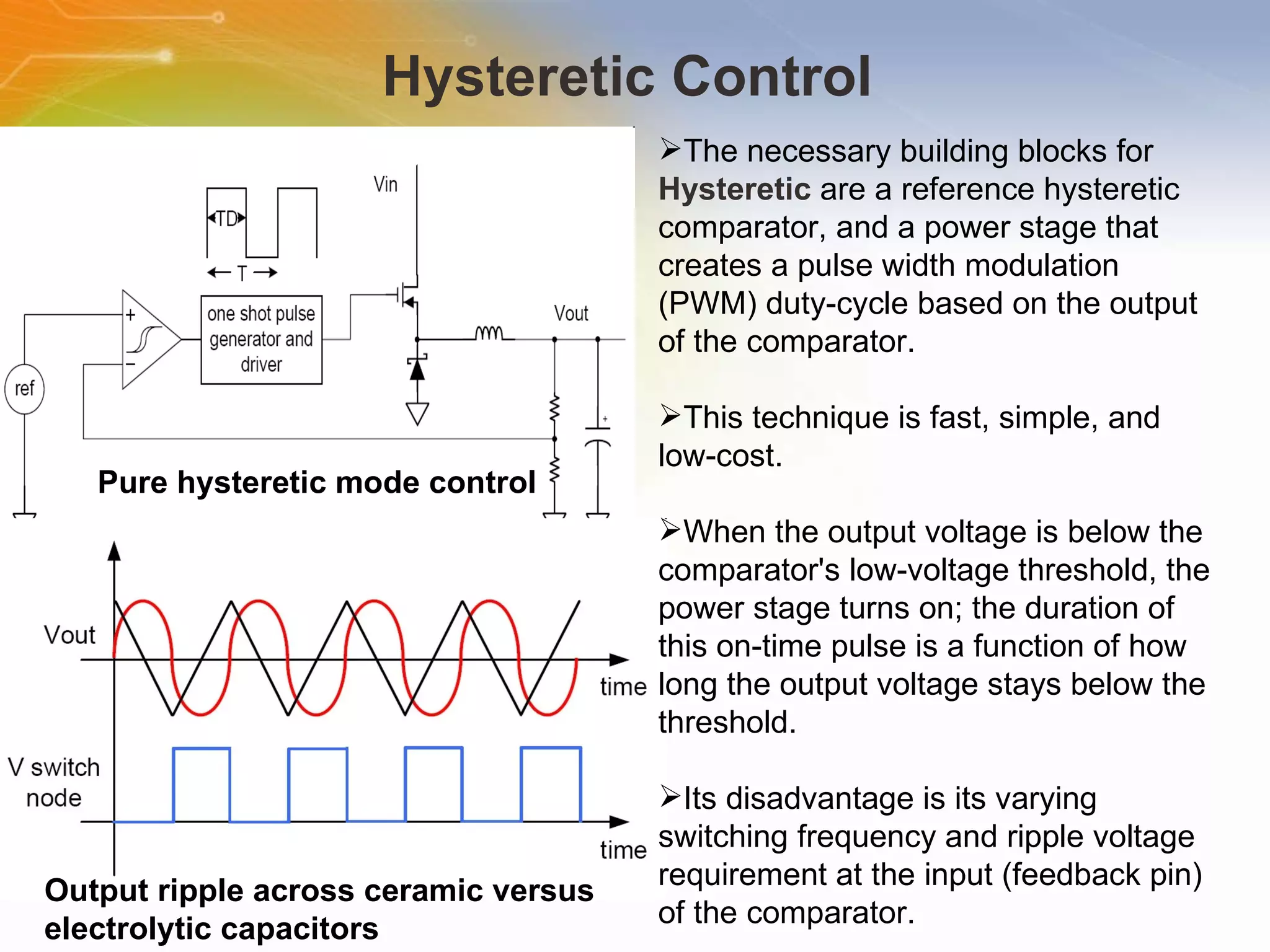
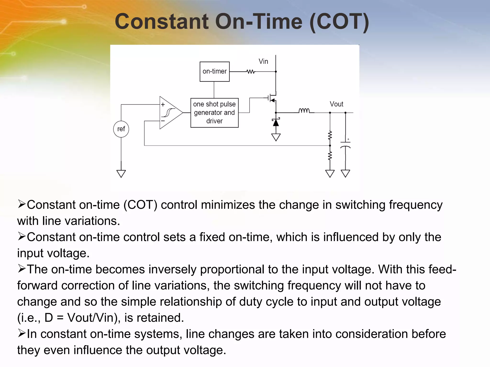
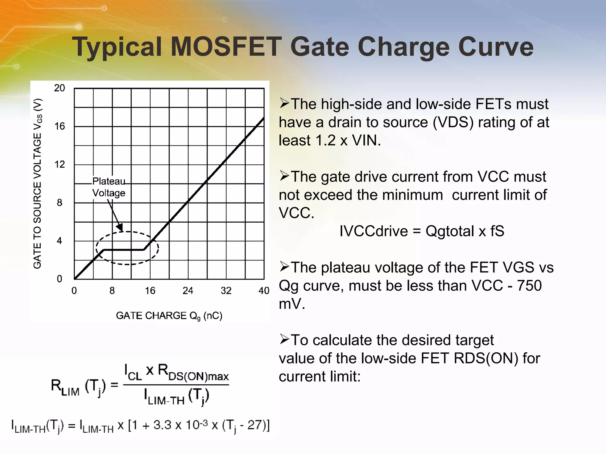
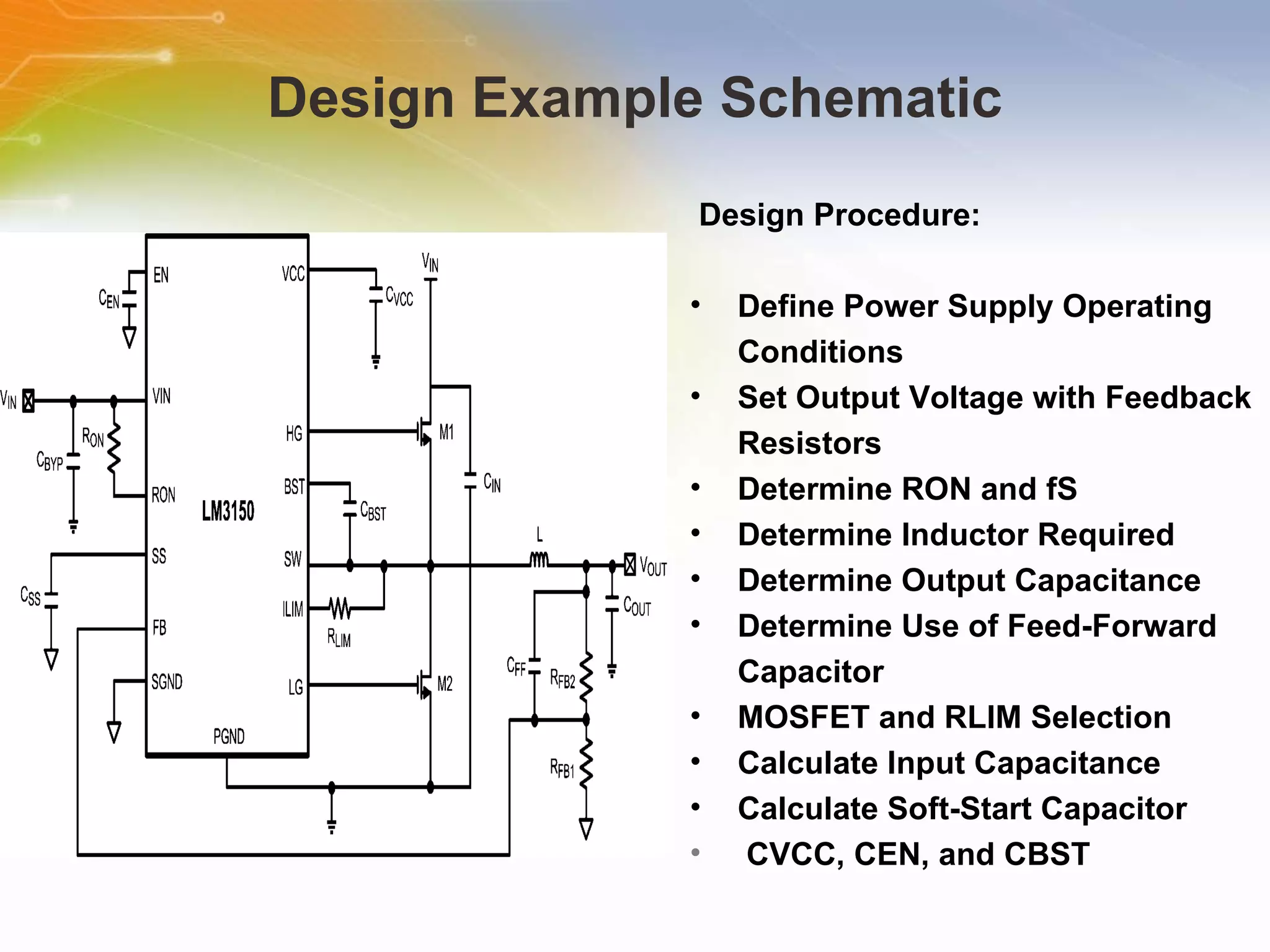
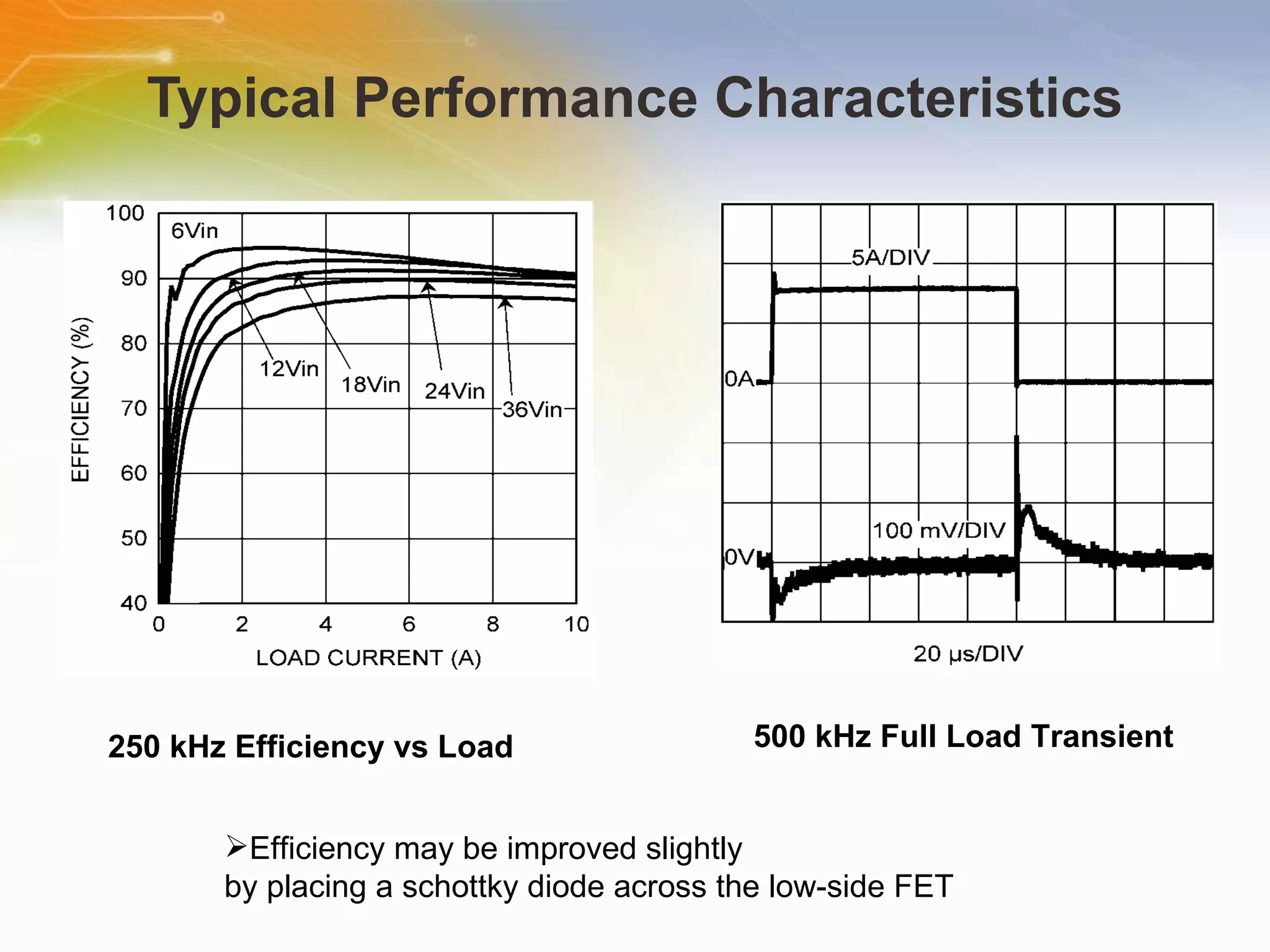
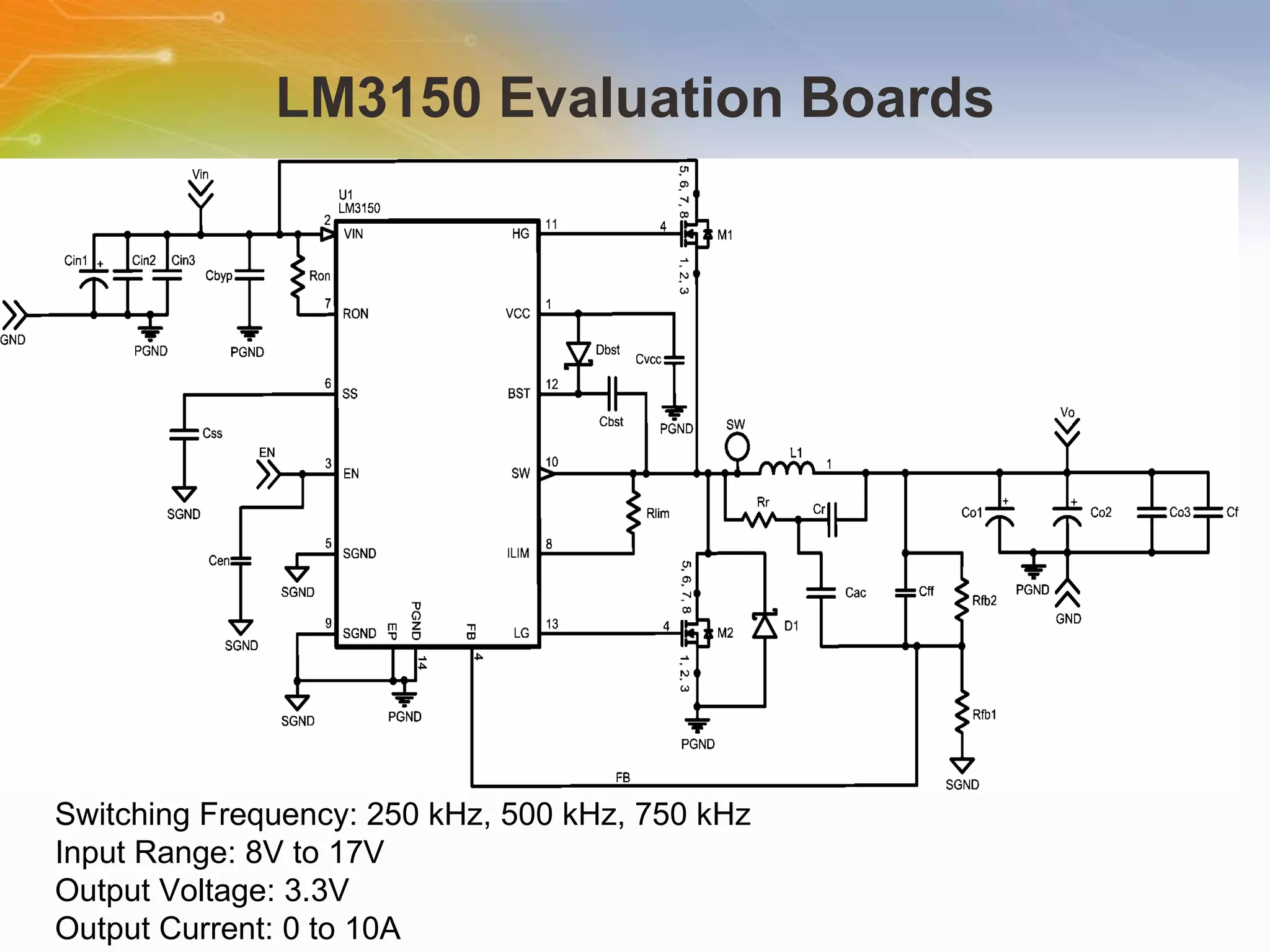
LM315x Synchronous Simple Switcher® Controller Series Source: National Semiconductor
Introduction Purpose An   overview   study   on   Synchronous   Simple   Switcher®   Controller   Series Outline Features,   Application   and   Performance Simplified   block   diagram Design   Example   schematic   and   its   parameter LM3150   Evaluation   Board   details Content 12   pages
Features  ■  PowerWise® step-down controller ■  6V to 42V Wide input voltage range ■  Adjustable output voltage down to 0.6V ■  Programmable switching frequency up to 1 MHz ■  No loop compensation required ■  Fully WEBENCH® enabled ■  Low external component count ■  Constant On-Time control ■  Ultra-fast transient response ■  Stable with low ESR capacitors ■  Output voltage pre-bias startup ■  Valley current limit ■  Programmable soft-start
Typical Applications ■  Telecom ■  Networking Equipment ■  Routers ■  Security Surveillance ■  Power Modules
Performance of LM3051 Output Current 12000 mA Input Min Voltage 6 Volt Input Max Voltage 42 Volt Feedback Voltage 0.6 Volt Feedback Tolerance 1.5 % Frequency Max 1000 kHz Efficiency (peak) 95 %
Simplified Block Diagram
Hysteretic Control  The   necessary   building   blocks   for   Hysteretic   are   a   reference   hysteretic   comparator,   and   a   power   stage   that   creates   a   pulse   width   modulation   (PWM)   duty-cycle   based   on   the   output   of   the   comparator.   This   technique   is   fast,   simple,   and   low-cost. When   the   output   voltage   is   below   the   comparator's   low-voltage   threshold,   the   power   stage   turns   on;   the   duration   of   this   on-time   pulse   is   a   function   of   how   long   the   output   voltage   stays   below   the   threshold.   Its   disadvantage   is   its   varying   switching   frequency   and   ripple   voltage   requirement   at   the   input   (feedback   pin)   of   the   comparator.   Pure hysteretic mode control   Output ripple across ceramic versus electrolytic capacitors
Constant On-Time (COT)  Constant   on-time   (COT)   control   minimizes   the   change   in   switching   frequency   with   line   variations. Constant   on-time   control   sets   a   fixed   on-time,   which   is   influenced   by   only   the   input   voltage.   The   on-time   becomes   inversely   proportional   to   the   input   voltage.   With   this   feed-forward   correction   of   line   variations,   the   switching   frequency   will   not   have   to   change   and   so   the   simple   relationship   of   duty   cycle   to   input   and   output   voltage   (i.e.,   D   =   Vout/Vin),   is   retained. In   constant   on-time   systems,   line   changes   are   taken   into   consideration   before   they   even   influence   the   output   voltage.
Typical MOSFET Gate Charge Curve The   high-side   and   low-side   FETs   must   have   a   drain   to   source   (VDS)   rating   of   at   least   1.2   x   VIN. The   gate   drive   current   from   VCC   must   not   exceed   the   minimum   current   limit   of   VCC. IVCCdrive   =   Qgtotal   x   fS The   plateau   voltage   of   the   FET   VGS   vs   Qg   curve,   must   be   less   than   VCC   -   750   mV. To   calculate   the   desired   target value   of   the   low-side   FET   RDS(ON)   for   current   limit:
Design Example Schematic Design   Procedure: Define   Power   Supply   Operating   Conditions Set   Output   Voltage   with   Feedback   Resistors Determine   RON   and   fS Determine   Inductor   Required Determine   Output   Capacitance Determine   Use   of   Feed-Forward   Capacitor MOSFET   and   RLIM   Selection Calculate   Input   Capacitance Calculate   Soft-Start   Capacitor CVCC,   CEN,   and   CBST
Typical Performance Characteristics 500 kHz Full Load Transient 250 kHz Efficiency vs Load Efficiency may be improved slightly by placing a schottky diode across the low-side FET
LM3150 Evaluation Boards Switching Frequency: 250 kHz, 500 kHz, 750 kHz Input Range: 8V to 17V Output Voltage: 3.3V Output Current: 0 to 10A
Additional Resource For ordering the LM315X, please click the part list or Call our sales hotline For additional inquires contact our technical service hotline For more product information go to http://www.national.com/analog/power/simple_switcher_lm315x Newark Farnell

LM315x Synchronous Simple Switcher® Controller Series

  • 1.
    LM315x Synchronous SimpleSwitcher® Controller Series Source: National Semiconductor
  • 2.
    Introduction Purpose An overview study on Synchronous Simple Switcher® Controller Series Outline Features, Application and Performance Simplified block diagram Design Example schematic and its parameter LM3150 Evaluation Board details Content 12 pages
  • 3.
    Features ■ PowerWise® step-down controller ■ 6V to 42V Wide input voltage range ■ Adjustable output voltage down to 0.6V ■ Programmable switching frequency up to 1 MHz ■ No loop compensation required ■ Fully WEBENCH® enabled ■ Low external component count ■ Constant On-Time control ■ Ultra-fast transient response ■ Stable with low ESR capacitors ■ Output voltage pre-bias startup ■ Valley current limit ■ Programmable soft-start
  • 4.
    Typical Applications ■ Telecom ■ Networking Equipment ■ Routers ■ Security Surveillance ■ Power Modules
  • 5.
    Performance of LM3051Output Current 12000 mA Input Min Voltage 6 Volt Input Max Voltage 42 Volt Feedback Voltage 0.6 Volt Feedback Tolerance 1.5 % Frequency Max 1000 kHz Efficiency (peak) 95 %
  • 6.
  • 7.
    Hysteretic Control The necessary building blocks for Hysteretic are a reference hysteretic comparator, and a power stage that creates a pulse width modulation (PWM) duty-cycle based on the output of the comparator. This technique is fast, simple, and low-cost. When the output voltage is below the comparator's low-voltage threshold, the power stage turns on; the duration of this on-time pulse is a function of how long the output voltage stays below the threshold. Its disadvantage is its varying switching frequency and ripple voltage requirement at the input (feedback pin) of the comparator. Pure hysteretic mode control Output ripple across ceramic versus electrolytic capacitors
  • 8.
    Constant On-Time (COT) Constant on-time (COT) control minimizes the change in switching frequency with line variations. Constant on-time control sets a fixed on-time, which is influenced by only the input voltage. The on-time becomes inversely proportional to the input voltage. With this feed-forward correction of line variations, the switching frequency will not have to change and so the simple relationship of duty cycle to input and output voltage (i.e., D = Vout/Vin), is retained. In constant on-time systems, line changes are taken into consideration before they even influence the output voltage.
  • 9.
    Typical MOSFET GateCharge Curve The high-side and low-side FETs must have a drain to source (VDS) rating of at least 1.2 x VIN. The gate drive current from VCC must not exceed the minimum current limit of VCC. IVCCdrive = Qgtotal x fS The plateau voltage of the FET VGS vs Qg curve, must be less than VCC - 750 mV. To calculate the desired target value of the low-side FET RDS(ON) for current limit:
  • 10.
    Design Example SchematicDesign Procedure: Define Power Supply Operating Conditions Set Output Voltage with Feedback Resistors Determine RON and fS Determine Inductor Required Determine Output Capacitance Determine Use of Feed-Forward Capacitor MOSFET and RLIM Selection Calculate Input Capacitance Calculate Soft-Start Capacitor CVCC, CEN, and CBST
  • 11.
    Typical Performance Characteristics500 kHz Full Load Transient 250 kHz Efficiency vs Load Efficiency may be improved slightly by placing a schottky diode across the low-side FET
  • 12.
    LM3150 Evaluation BoardsSwitching Frequency: 250 kHz, 500 kHz, 750 kHz Input Range: 8V to 17V Output Voltage: 3.3V Output Current: 0 to 10A
  • 13.
    Additional Resource Forordering the LM315X, please click the part list or Call our sales hotline For additional inquires contact our technical service hotline For more product information go to http://www.national.com/analog/power/simple_switcher_lm315x Newark Farnell

Editor's Notes

  • #2 Welcome to the training module on the LM3150 Synchronous Simple Switcher Controller.
  • #3 In this module, we will discuss the feature, application and performance characteristics of the LM315X device. We will also go over block diagrams, examples of schematics and the eval board.
  • #4 The LM3150 SIMPLE SWITCHER® Controller is an easy to use and simplified step down power controller, capable of providing up to 12A of output current in a typical application. Operating with an input voltage range of 6V-42V, the LM3150 features an adjustable output voltage down to 0.6V. The switching frequency is adjustable up to 1 MHz and the synchronous architecture provides for highly efficient designs. The LM3150 controller employs a Constant On-Time (COT) architecture with a proprietary Emulated Ripple Mode (ERM) control that allows for the use of low ESR output capacitors, which reduces overall solution size and output voltage ripple. The Constant On-Time (COT) regulation architecture allows for fast transient response and requires no loop compensation, which reduces external component count and reduces design complexity.
  • #5 This device can go into various application areas like Telecom, Networking equipment, routers, security surveillance and power modules.
  • #6 This chart lists the key performance specification of the LM3051 device. The device can deliver a maximum current output of 12A, a max input voltage of 42 volts, a max operating frequency of 1MHz and with a 95% of Efficiency.
  • #7 The LM3150 synchronous step-down SIMPLE SWITCHER Controller utilizes a Constant On-Time (COT) architecture which is a derivative of the hysteretic control scheme. COT relies on a fixed switch on-time to regulate the output. The on-time of the high-side switch can be set manually by adjusting the size of an external resistor (RON). To maintain a relatively constant switching frequency as VIN varies, the LM3150 automatically adjusts the on-time inversely with the input voltage. Assuming an ideal system and VIN is much greater than 1V. Control is based on a comparator and the on-timer, with the output voltage feedback (FB) compared with an internal reference of 0.6V. If the FB level is below the reference, the high side switch is turned on for a fixed time, tON, which is determined by the input voltage and the resistor RON. Following this on-time, the switch remains off for a minimum off-time, tOFF, as specified in the Electrical Characteristics table or until the FB pin voltage is below the reference, then the switch turns on again for another on-time period. The switching will continue in this fashion to maintain regulation. During continuous conduction mode (CCM), the switching frequency ideally depends on duty-cycle and on-time only.
  • #8 When the output voltage is below the comparator's low-voltage threshold, the power stage turns on; the duration of this on-time pulse is a function of how long the output voltage stays below the threshold. As a result, the pulse frequency is not constant, but depends on how the output voltage changes during both the on-time and off-time. Hysteretic control does not require an internal oscillator. Switching frequency depends on the external components and operating conditions such as load current and line voltage, since these parameters influence when the output voltage crosses the hysteretic comparator thresholds.
  • #9 Constant on-time (COT) control minimizes the change in switching frequency with line variations, which, depending on the particular hysteretic design, would otherwise vary the switching frequency significantly and create many problems. Constant on-time control sets a fixed on-time, which is influenced by input voltage. The on-time becomes inversely proportional to the input voltage. With this feed-forward correction of line variations, the switching frequency will not have to change and as such, the simple relationship of duty cycle to input and output voltage (i.e., D = Vout/Vin), is retained.
  • #10 This slide shows you the Typical MOSFET, Gate Charge Curve which is obtained by considering the proper component values for R sub limit and Rds(on). The gate drive current from VCC must not exceed the minimum current limit of VCC.
  • #11 The design guide provides the equations required to design with the LM3150 SIMPLE SWITCHER® Controller. The WEBENCH® design tool can be used with, or in place of this section. We have given the steps for how to design with LM3150 device: The available frequency range for a given input voltage range, is determined by the duty-cycle or Vout/Vin and the minimum On-time and OFF-time.
  • #12 This is a typical performance characteristics of the device family. The first graphs shows the Efficiency vs load curve at 250 KHz and the 2 nd shows it at 500kHz.
  • #13 The LM3150 evaluation boards are designed to provide the design engineer with a fully functional power converter, based on Constant On-Time and with Emulated Ripple mode control to evaluate the LM3150 and the entire LM315x family of parts. The evaluation board is pre-configured to use the LM3150 with the output voltage pre-set to 3.3V, and a typical max load current of 10A. There are three different boards that are configured for 250 kHz, 500 kHz, and 750 kHz respectively. The evaluation board allows for a variety of configurations, and this multifunctional capability is used to also accept the fixed output versions of the LM3150 such as the LM3151-3.3, LM3152-3.3, and the LM3153-3.3.
  • #14 Thank you for taking the time to view this presentation on LM315X. If you would like to learn more or go on to purchase some of these devices, you may either click on the part list link, or simple call our sales hotline. For more technical information you may either visit the National Semiconductor site, or if you would prefer to speak to someone live, please call our hotline number, or even use our ‘live chat’ online facility.