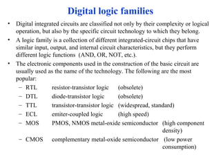
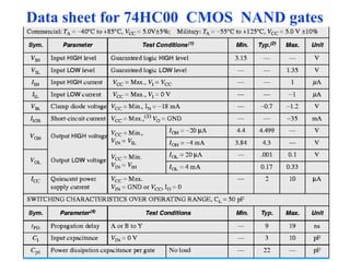
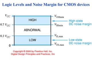
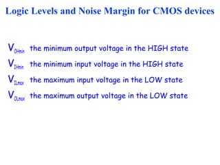
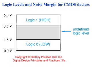
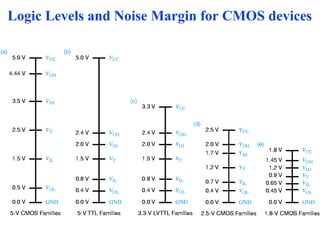
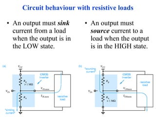
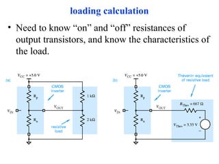
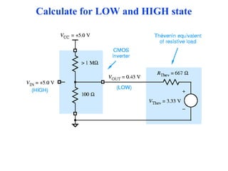
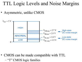
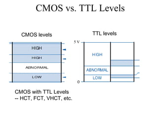
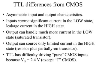
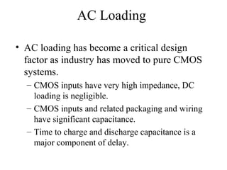
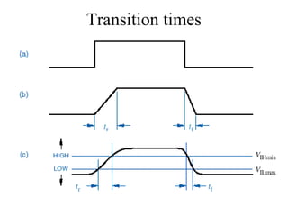
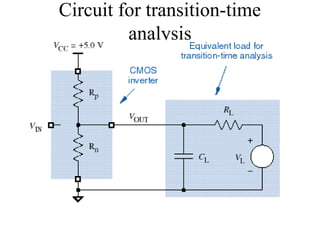
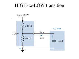
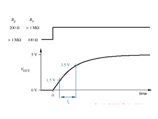
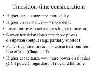
Digital logic
families
Digital logic families
• Digital integrated circuits are classified not only by their complexity or logical
operation, but also by the specific circuit technology to which they belong.
• A logic family is a collection of different integrated-circuit chips that have
similar input, output, and internal circuit characteristics, but they perform
different logic functions (AND, OR, NOT, etc.).
• The electronic components used in the construction of the basic circuit are
usually used as the name of the technology. The following are the most
popular:
– RTL resistor-transistor logic (obsolete)
– DTL diode-transistor logic (obsolete)
– TTL transistor-transistor logic (widespread, standard)
– ECL emiter-coupled logic (high speed)
– MOS PMOS, NMOS metal-oxide semiconductor (high component
density)
– CMOS complementary metal-oxide semiconductor (low power
consumption)
Various series of the TTL Logic family
TTL Series Prefix Example
Standard TTL 74 7486
High-speed TTL 74H 74H86
Low-power TTL 74L 74L86
Schottky TTL 74S 74S86
Low-power Schottky TTL 74LS 74LS86
Advanced Schottky TTL 74AS 74AS86
Advanced Low-power Schottky TTL 74ALS 74ALS86
Various series of the CMOS Logic family
CMOS Series Prefix Example
Original CMOS 40 4009
Pin compatible with TTL 74C 74H04
High-speed and pin compatible with TTL 74HC 74HC04
High-speed and electrically compatible with TTL 74HCT 74HCT04
Very High-speed and pin compatible with TTL 74VHC 74VHC04
Very High-speed and electrically compatible with TTL 74VHCT 74VHCT04
Advanced High-speed and pin compatible with TTL 74AHC 74AHC04
Advanced High-speed and electrically compatible with TTL 74AHCT 74AHCT04
Fast and electrically compatible with TTL 74FCT 74 FCT 04
Fast and electrically compatible with TTL with TTL VOH 74FCT-T 74 FCT04T
Why NAND and NOR are so popular?
• Logical inversion comes free as a result an inverting gate needs
smaller number of transistors compared to the non-inverting one.
• In CMOS, and in most other logic families, the simples gates are
inverters, and the next simplest are NAND and Nor gates.
CMOS NAND Gates
• Use 2n transistors for n-input gate
• 2-input AND gate:
Electrical Characteristics
• The characteristics of digital logic families are usually compared
by analyzing the circuit of the basic gate in each family:
• the most important parameters are:
• fan-out specifies the number of standard loads that the output can
drive without impairing its normal operation.
• A standard load is usually defined as the amount of current needed
by an input of another similar gate of the same family.
• Power dissipation is the power consumed by the gate
• propagation delay is the average transition delay time for the
signal to propagate from input to output.
• Noise margin is the minimum external noise vo,ltage that causes
an undesirable change in the circuit output.
Data sheet for 74HC00 CMOS NAND gates
Logic Levels and Noise Margin for CMOS devices
VOHmin the minimum output voltage in the HIGH state
VIHmin the minimum input voltage in the HIGH state
VILmax the maximum input voltage in the LOW state
VOLmax the maximum output voltage in the LOW state
Logic Levels and Noise Margin for CMOS devices
Circuit behaviour with resistive loads
• An output must sink
current from a load
when the output is in
the LOW state.
• An output must
source current to a
load when the output
is in the HIGH state.
loading calculation
• Need to know “on” and “off” resistances of
output transistors, and know the characteristics of
the load.
Calculate for LOW and HIGH state
Output-voltage drops
• Resistance of “off” transistor is > 1
Megaohm, but resistance of “on” transistor
is nonzero,
– Voltage drops across “on” transistor, V = IR
• For “CMOS” loads, current and voltage
drop are negligible.
• For TTL inputs, LEDs, terminations, or
other resistive loads, current and voltage
drop are significant and must be calculated.
Calculate for LOW and HIGH state
Limitation on DC load
• If too much load, output voltage will go
outside of valid logic-voltage range.
Output-drive specs
• VOLmax and VOHminare specified for certain output-
current values, IOLmax and IOHmax.
– No need to know details about the output circuit, only
the load.
Input-loading specs
• Each gate input requires a certain amount of current
to drive it in the LOW state and in the HIGH state.
– IIL and IIH
– These amounts are specified by the manufacturer.
• Fanout calculation
– (LOW state) The sum of the IIL values of the driven inputs
may not exceed IOLmax of the driving output.
– (HIGH state) The sum of the IIH values of the driven inputs
may not exceed IOHmax of the driving output.
– Need to do Thevenin-equivalent calculation for non-gate
loads (LEDs, termination resistors, etc.)
TTL Electrical Characteristics
TTL LOW-State Behavior
TTL HIGH-State Behavior
TTL Logic Levels and Noise Margins
• Asymmetric, unlike CMOS
• CMOS can be made compatible with TTL
– “T” CMOS logic families
CMOS vs. TTL Levels
CMOS levels TTL levels
CMOS with TTL Levels
-- HCT, FCT, VHCT, etc.
TTL differences from CMOS
• Asymmetric input and output characteristics.
• Inputs source significant current in the LOW state,
leakage current in the HIGH state.
• Output can handle much more current in the LOW
state (saturated transistor).
• Output can source only limited current in the HIGH
state (resistor plus partially-on transistor).
• TTL has difficulty driving “pure” CMOS inputs
because VOH = 2.4 V (except “T” CMOS).
AC Loading
• AC loading has become a critical design
factor as industry has moved to pure CMOS
systems.
– CMOS inputs have very high impedance, DC
loading is negligible.
– CMOS inputs and related packaging and wiring
have significant capacitance.
– Time to charge and discharge capacitance is a
major component of delay.
Transition times
Circuit for transition-time
analysis
HIGH-to-LOW transition
Exponential rise time
LOW-to-HIGH transition
Exponential fall time
t = RC time constant
exponential formulas, e-t/RC
Transition-time considerations
• Higher capacitance ==> more delay
• Higher on-resistance ==> more delay
• Lower on-resistance requires bigger transistors
• Slower transition times ==> more power
dissipation (output stage partially shorted)
• Faster transition times ==> worse transmission-
line effects (Chapter 11)
• Higher capacitance ==> more power dissipation
(CV2
f power), regardless of rise and fall time
Open-drain outputs
• No PMOS transistor, use resistor pull-up
What good is it?
• Open-drain bus
• Problem -- really bad rise time
Open-drain transition times
• Pull-up resistance is larger than a PMOS
transistor’s “on” resistance.
• Can reduce rise time by reducing pull-up resistor
value
– But not too much

digital logic_families

  • 1.
  • 2.
    Digital logic families •Digital integrated circuits are classified not only by their complexity or logical operation, but also by the specific circuit technology to which they belong. • A logic family is a collection of different integrated-circuit chips that have similar input, output, and internal circuit characteristics, but they perform different logic functions (AND, OR, NOT, etc.). • The electronic components used in the construction of the basic circuit are usually used as the name of the technology. The following are the most popular: – RTL resistor-transistor logic (obsolete) – DTL diode-transistor logic (obsolete) – TTL transistor-transistor logic (widespread, standard) – ECL emiter-coupled logic (high speed) – MOS PMOS, NMOS metal-oxide semiconductor (high component density) – CMOS complementary metal-oxide semiconductor (low power consumption)
  • 3.
    Various series ofthe TTL Logic family TTL Series Prefix Example Standard TTL 74 7486 High-speed TTL 74H 74H86 Low-power TTL 74L 74L86 Schottky TTL 74S 74S86 Low-power Schottky TTL 74LS 74LS86 Advanced Schottky TTL 74AS 74AS86 Advanced Low-power Schottky TTL 74ALS 74ALS86
  • 4.
    Various series ofthe CMOS Logic family CMOS Series Prefix Example Original CMOS 40 4009 Pin compatible with TTL 74C 74H04 High-speed and pin compatible with TTL 74HC 74HC04 High-speed and electrically compatible with TTL 74HCT 74HCT04 Very High-speed and pin compatible with TTL 74VHC 74VHC04 Very High-speed and electrically compatible with TTL 74VHCT 74VHCT04 Advanced High-speed and pin compatible with TTL 74AHC 74AHC04 Advanced High-speed and electrically compatible with TTL 74AHCT 74AHCT04 Fast and electrically compatible with TTL 74FCT 74 FCT 04 Fast and electrically compatible with TTL with TTL VOH 74FCT-T 74 FCT04T
  • 5.
    Why NAND andNOR are so popular? • Logical inversion comes free as a result an inverting gate needs smaller number of transistors compared to the non-inverting one. • In CMOS, and in most other logic families, the simples gates are inverters, and the next simplest are NAND and Nor gates.
  • 6.
    CMOS NAND Gates •Use 2n transistors for n-input gate
  • 7.
  • 8.
    Electrical Characteristics • Thecharacteristics of digital logic families are usually compared by analyzing the circuit of the basic gate in each family: • the most important parameters are: • fan-out specifies the number of standard loads that the output can drive without impairing its normal operation. • A standard load is usually defined as the amount of current needed by an input of another similar gate of the same family. • Power dissipation is the power consumed by the gate • propagation delay is the average transition delay time for the signal to propagate from input to output. • Noise margin is the minimum external noise vo,ltage that causes an undesirable change in the circuit output.
  • 9.
    Data sheet for74HC00 CMOS NAND gates
  • 10.
    Logic Levels andNoise Margin for CMOS devices
  • 11.
    Logic Levels andNoise Margin for CMOS devices VOHmin the minimum output voltage in the HIGH state VIHmin the minimum input voltage in the HIGH state VILmax the maximum input voltage in the LOW state VOLmax the maximum output voltage in the LOW state
  • 12.
    Logic Levels andNoise Margin for CMOS devices
  • 13.
    Logic Levels andNoise Margin for CMOS devices
  • 14.
    Circuit behaviour withresistive loads • An output must sink current from a load when the output is in the LOW state. • An output must source current to a load when the output is in the HIGH state.
  • 15.
    loading calculation • Needto know “on” and “off” resistances of output transistors, and know the characteristics of the load.
  • 16.
    Calculate for LOWand HIGH state
  • 17.
    Output-voltage drops • Resistanceof “off” transistor is > 1 Megaohm, but resistance of “on” transistor is nonzero, – Voltage drops across “on” transistor, V = IR • For “CMOS” loads, current and voltage drop are negligible. • For TTL inputs, LEDs, terminations, or other resistive loads, current and voltage drop are significant and must be calculated.
  • 18.
    Calculate for LOWand HIGH state
  • 19.
    Limitation on DCload • If too much load, output voltage will go outside of valid logic-voltage range.
  • 20.
    Output-drive specs • VOLmaxand VOHminare specified for certain output- current values, IOLmax and IOHmax. – No need to know details about the output circuit, only the load.
  • 21.
    Input-loading specs • Eachgate input requires a certain amount of current to drive it in the LOW state and in the HIGH state. – IIL and IIH – These amounts are specified by the manufacturer. • Fanout calculation – (LOW state) The sum of the IIL values of the driven inputs may not exceed IOLmax of the driving output. – (HIGH state) The sum of the IIH values of the driven inputs may not exceed IOHmax of the driving output. – Need to do Thevenin-equivalent calculation for non-gate loads (LEDs, termination resistors, etc.)
  • 22.
  • 23.
  • 24.
  • 25.
    TTL Logic Levelsand Noise Margins • Asymmetric, unlike CMOS • CMOS can be made compatible with TTL – “T” CMOS logic families
  • 26.
    CMOS vs. TTLLevels CMOS levels TTL levels CMOS with TTL Levels -- HCT, FCT, VHCT, etc.
  • 27.
    TTL differences fromCMOS • Asymmetric input and output characteristics. • Inputs source significant current in the LOW state, leakage current in the HIGH state. • Output can handle much more current in the LOW state (saturated transistor). • Output can source only limited current in the HIGH state (resistor plus partially-on transistor). • TTL has difficulty driving “pure” CMOS inputs because VOH = 2.4 V (except “T” CMOS).
  • 28.
    AC Loading • ACloading has become a critical design factor as industry has moved to pure CMOS systems. – CMOS inputs have very high impedance, DC loading is negligible. – CMOS inputs and related packaging and wiring have significant capacitance. – Time to charge and discharge capacitance is a major component of delay.
  • 29.
  • 30.
  • 31.
  • 32.
  • 33.
  • 34.
    Exponential fall time t= RC time constant exponential formulas, e-t/RC
  • 35.
    Transition-time considerations • Highercapacitance ==> more delay • Higher on-resistance ==> more delay • Lower on-resistance requires bigger transistors • Slower transition times ==> more power dissipation (output stage partially shorted) • Faster transition times ==> worse transmission- line effects (Chapter 11) • Higher capacitance ==> more power dissipation (CV2 f power), regardless of rise and fall time
  • 36.
    Open-drain outputs • NoPMOS transistor, use resistor pull-up
  • 37.
    What good isit? • Open-drain bus • Problem -- really bad rise time
  • 38.
    Open-drain transition times •Pull-up resistance is larger than a PMOS transistor’s “on” resistance. • Can reduce rise time by reducing pull-up resistor value – But not too much