SlideShare a Scribd company logo
VLSI Design MCQs
Unit No. 1
1. What is the full form of VHDL?
a) Verilog Hardware Description Language
b) Very High speed Description Language
c) Variable Hardware Description Language
d) Very high speed Hardware Description Language
2. What is the basic use of EDA tools?
a) Communication of Electronic devices
b) Fabrication of Electronics hardware
c) Electronic circuits simulation and synthesis
d) Industrial automation
3. After compiling VHDL code with any EDA tool, we get __________
a) Final device
b) FPGA
c) Optimized netlist
d) Netlist
4. Which of the following is not an EDA tool?
a) Visual C++
b) Quartus II
c) Xilinx ISE
d) MaxPlus II
5. The process of transforming a design entry information of the circuit into a set of
logic equations in any EDA tool is known as _________
a) Simulation
b) Synthesis
c) Optimization
d) Verification
6. Place and Route EDA tools are used to take the design netlist and implement the
design in the device.
a) True
b) False
7. Which of the following is not a back end EDA tool?
a) Floor planning tools
b) Placement tools
c) Routing tools
d) Simulators
8. Difference between simulation tools and Synthesis tool is _________
a) Simulators are used to check the performance of circuit and Synthesis tools are for the
fabrication of circuits
b) Simulators and Synthesis tools works exactly same
c) Simulators are used just to check basic functionality of the circuit and Synthesis tools
includes timing constraints and other factors along with simulation
d) Simulation finds the error in the code and Synthesis tool corrects the code
9. What is the extension of the Netlist file; input to the place and route EDA tools?
a) EIDF
b) SDF
c) TXT
d) CPP
10. Which of the following is the basic building block of a design?
a) Architecture
b) Entity
c) Process
d) Package
11. A package in VHDL consists of _________
a) Commonly used architectures
b) Commonly used tools
c) Commonly used data types and subroutines
d) Commonly used syntax and variables
12. Complete description of the circuit to be designed is given in _________
a) Architecture
b) Entity
c) Library
d) Configurations
13. An entity can have more than one architecture.
a) True
b) False
14. Predefined data for an VHDL object is called ________
a) Generic
b) Constant
c) Attribute
d) Library
15. A process is the basic unit of execution in VHDL.
a) True
b) False
16. Which of the following describes the structure of VHDL code correctly?
a) Library Declaration; Entity Declaration; Architecture Declaration; Configurations
b) Entity Declaration; Configuration; Library Declaration; Architecture Declaration
c) Configuration; Library Declaration; Entity Declaration; Architecture Declaration
d) Library Declaration; Configuration; Entity Declaration; Architecture Declaration
17. Which of the following statement is true?
a) Package is a collection of Libraries
b) Library is a collection of Packages
c) Entity is a collection of Packages
d) Architecture is a collection of Entities
18. What does modeling type refer to?
a) Type of ports in entity block of VHDL code
b) Type of description statements in architecture block of VHDL code
c) Type of data objects
d) Type of Signals
19. Which of the following is not a type of VHDL modeling?
a) Behavioral modeling
b) Dataflow modeling
c) Structural modeling
d) Component modeling
20. In behavioral modeling, what do descriptive statements describe?
a) How the system performs on given input values
b) How the design is to be implemented
c) Netlist
d) Concurrent execution
21. Which of the following statement is used in structural modeling?
a) portmap
b) process
c) if-else
d) case
22. What is the basic unit of behavioral description?
a) Structure
b) Sequence
c) Process
d) Dataflow
23. Which of the following modeling style follows the sequential processing of
instructions?
a) Dataflow modeling
b) Behavior modeling
c) Structural modeling
d) Component modeling
24. ______modeling uses logic gates and basic blocks to describe the functionality of
system.
a) Behavioral
b) Structural
c) Dataflow
d) Component
Unit No. 2
1. Which sequential circuits generate the feedback path due to the cross-coupled
connection from output of one gate to the input of another gate?
a) Synchronous
b) Asynchronous
c) Both
d) None of the above
2. What is/are the crucial function/s of memory elements used in the sequential
circuits?
a) Storage of binary information
b) Specify the state of sequential
c) Both a & b
d) None of the above
3. How are the sequential circuits specified in terms of time sequence?
a) By Inputs
b) By Outputs
c) By Internal states
d) All of the above
4. The behavior of synchronous sequential circuit can be predicted by defining the
signals at ______.
a) discrete instants of time
b) continuous instants of time
c) sampling instants of time
d) at any instant of time
5. Which memory elements are utilized in an asynchronous & clocked sequential
circuits respectively?
a) Time- delay devices & registers
b) Time- delay devices & flip-flops
c) Time- delay devices & counters
d) Time-delay devices & latches
6. Why do the D-flipflops receives its designation or nomenclature as 'Data Flipflops'
a) Due to its capability to receive data from fliflop
b) Due to its capability to store data in flipflop
c) Due to its capability to transfer the data into flipflop
d) All of the above
7. The characteristic equation of D-flipflop implies that _____.
a) the next state is dependent on previous state
b) the next state is dependent on present state
c) the next state is independent of previous state
d) the next state is independent of present state
8. Which circuit is generated from D-flipflop due to addition of an inverter by causing
reduction in the number of inputs?
a) Gated JK- latch
b) Gated SR- latch
c) Gated T- latch
d) Gated D- latch
9. According to Moore circuit, the output of synchronous sequential circuit depend/s
on ______ of flip flop
a) Past state
b) Present state
c) Next state
d) External inputs
10. Which type of memory elements are used in synchronous sequential circuits?
a) Clocked Flip flops
b) Unclocked Flip flops
c) Time Delay Elements
d) All of the above
Unit No. 3
1. Which is used to control the scan path movement?
a) clock signals
b) input signals
c) output signals
d) delay signals
2. Boundary scan test is used to test
a) pins
b) multipliers
c) boards
d) wires
3. The boundary scan path is provided with
a) serial input outputs pads
b) parallel input pads
c) parallel output pads
d) buffer pads
4. The boundary scan path tests the
a) input nodes
b) output nodes
c) buffer nodes
d) interconnection points
5. Boundary scan method takes lesser time on test pattern generation.
a) true
b) false
6. The disadvantage of boundary scan method is that the fault coverage is less.
a) true
b) false
7. In scan/set method, __________ is used to implement a scan path
a) serial registers
b) storage elements
c) parallel registers
d) separate register
Unit No. 4
1. nMOS devices are formed in
a) p-type substrate of high doping level
b) n-type substrate of low doping level
c) p-type substrate of moderate doping level
d) n-type substrate of high doping level
2. Source and drain in nMOS device are isolated by
a) a single diode
b) two diodes
c) three diodes
d) four diodes
3. In depletion mode, source and drain are connected by
a) insulating channel
b) conducing channel
c) Vdd
d) Vss
4. The condition for non saturated region is
a) Vds = Vgs – Vt
b) Vgs lesser than Vt
c) Vds lesser than Vgs – Vt
d) Vds greater than Vgs – Vt
5. In enhancement mode, device is in _________ condition
a) conducting
b) non conducting
c) partially conducting
d) insulating
6. The condition for non conducting mode is
a) Vds lesser than Vgs
b) Vgs lesser than Vds
c) Vgs = Vds = 0
d) Vgs = Vds = Vs = 0
7. nMOS is
a) donor doped
b) acceptor doped
c) all of the mentioned
d) none of the mentioned
8. MOS transistor structure is
a) symmetrical
b) non symmetrical
c) semi symmetrical
d) pseudo symmetrical
9. Inversion layer in enhancement mode consists of excess of
a) holes
b) electrons
c) both in equal quantity
d) neutral carriers
10. The condition for linear region is
a) Vgs lesser than Vt
b) Vgs greater than Vt
c) Vds lesser than Vgs
d) Vds greater than Vgs
11. As source drain voltage increases, channel depth
a) increases
b) decreases
c) logarithmically increases
d) exponentially increases
12. The enhancement MOSFET is
a) Normally off MOSFET
b) Useful as a very good constant voltage source
c) Widely used because of easy in its fabrication
d) Normally on MOSFET
13. The depletion N-channel MOSFET
a) Can be operated as a JFET with zero gate voltage
b) Can be operated as an enhancement MOSFET by applying +ve bias to gate
c) Can be operated as an enhancement MOSFET by applying -ve bias to gate
d) Cannot be operated as an enhancement MOSFET
Unit No. 5
1. In accordance to the scaling technology, the total delay of the logic circuit depends
on ______
a) The capacitor to be charged
b) The voltage through which capacitance must be charged
c) Available current
d) All of the above
2. In CMOS circuits, which type of power dissipation occurs due to switching of
transient current and charging & discharging of load capacitance?
a) Static dissipation
b) Dynamic dissipation
c) Both a and b
d) None of the above
3. In high noise margin (NMH), the difference in magnitude between the maximum
HIGH output voltage of driving gate and the maximum HIGH voltage is recognized by
the _________gate.
a) Driven
b) Receiving
c) Both a and b
d) None of the above
4. Which factor/s play/s a crucial role in determining the speed of CMOS logic gate?
a) Load capacitance
b) Supply voltage
c) Gain factor of MOS
d) All of the above
5. For complex gate design in CMOS, OR function needs to be implemented by _______
connection/s of MOS.
a) Series
b) Parallel
c) Both series and parallel
d) None of the above
6. In pull-up network, PMOS transistors of CMOS are connected in parallel with the
provision of conducting path between output node & Vdd yielding _____ output.
a) 1
b) 0
c) Both a and b
d) None of the above
7. In CMOS inverter, the propagation delay of a gate is the/an _________ transition delay
time for the signal during propagation from input to output especially when the
signal changes its value.
a) Highest
b) Average
c) Lowest
d) None of the above
8. In enhancement MOSFET, the magnitude of output current __________ due to an
increase in the magnitude of gate potentials.
a) Increases
b) Remains constant
c) Decreases
d) None of the above
9. Which type of MOSFET exhibits no current at zero gate voltage?
a) Depletion MOSFET
b) Enhancement MOSFET
c) Both a and b
d) None of the above
Unit No. 6
1. Simple Programmable Logic Devices (SPLDs) are also regarded as ________.
a) Programmable Array Logic (PAL)
b) Generic Array Logic (GAL)
c) Programmable Logic Array (PLA)
d) All of the above
2. Which among the following is/are not suitable for in-system programming?
a) EPROM
b) EEPROM
c) Flash
d) All of the above
3. The devices which are based on fusible link or anti-fuse are _________time/s
programmable.
a) one
b) two
c) four
d) infinite
4. Which programming technology/ies is/are predominantly associated with SPLDs
and CPLDs?
a) EPROM
b) EEPROM
c) FLASH
d) All of the above
5. An Antifuse programming technology is predominantly associated with _____
a) SPLDs
b) FPGAs
c) CPLDs
d) All of the above
6. FPGA devices are________type
a) PLD
b) EPROM
c) SROM
d) SLD
7. FPGS Stands for________
a) Field Programmable gate array
b) First Programmable gate array
c) Field Program gate array
d) First Program gate array
8. Vertical and horizontal directions in FPGA are separated by________
a) A channel
b) A line
c) A strobe
d) A gap
………………………………….All the Best………………………………….

More Related Content

What's hot

Verilog HDL
Verilog HDLVerilog HDL
Verilog HDL
Mantra VLSI
 
2016 03-03 marchand
2016 03-03 marchand2016 03-03 marchand
2016 03-03 marchand
SCEE Team
 
Dsd lab Practical File
Dsd lab Practical FileDsd lab Practical File
Dsd lab Practical File
Soumya Behera
 
Lecture 2 verilog
Lecture 2   verilogLecture 2   verilog
Lecture 2 verilogvenravi10
 
Vlsilab13
Vlsilab13Vlsilab13
Vlsilab13Krish s
 
EuroMPI 2019: Multilevel Checkpointing for MPI Applications
EuroMPI 2019: Multilevel Checkpointing for MPI ApplicationsEuroMPI 2019: Multilevel Checkpointing for MPI Applications
EuroMPI 2019: Multilevel Checkpointing for MPI Applications
LEGATO project
 
Verilog VHDL code Decoder and Encoder
Verilog VHDL code Decoder and EncoderVerilog VHDL code Decoder and Encoder
Verilog VHDL code Decoder and Encoder
Bharti Airtel Ltd.
 
Modules and ports in Verilog HDL
Modules and ports in Verilog HDLModules and ports in Verilog HDL
Modules and ports in Verilog HDL
anand hd
 
microprocessor Questions with solution
microprocessor Questions with solutionmicroprocessor Questions with solution
microprocessor Questions with solution
dit
 
Digital electronics revision unit4 mcq
Digital electronics revision unit4  mcqDigital electronics revision unit4  mcq
Digital electronics revision unit4 mcq
SIVALAKSHMIPANNEERSE
 
400-101 Updated Question Answer
400-101 Updated Question Answer400-101 Updated Question Answer
400-101 Updated Question Answer
wrouthae
 
Gate-Cs 1992
Gate-Cs 1992Gate-Cs 1992
Gate-Cs 1992
Ravi Rajput
 
Basics of digital verilog design(alok singh kanpur)
Basics of digital verilog design(alok singh kanpur)Basics of digital verilog design(alok singh kanpur)
Basics of digital verilog design(alok singh kanpur)
Alok Singh
 
Introduction to FPGA, VHDL
Introduction to FPGA, VHDL  Introduction to FPGA, VHDL
Introduction to FPGA, VHDL
Amr Rashed
 
AN EFFICIENT BASE-4 LEADING ZERO DETECTOR DESIGN
AN EFFICIENT BASE-4 LEADING ZERO DETECTOR DESIGNAN EFFICIENT BASE-4 LEADING ZERO DETECTOR DESIGN
AN EFFICIENT BASE-4 LEADING ZERO DETECTOR DESIGN
EEIJ journal
 

What's hot (16)

Verilog HDL
Verilog HDLVerilog HDL
Verilog HDL
 
2016 03-03 marchand
2016 03-03 marchand2016 03-03 marchand
2016 03-03 marchand
 
Dsd lab Practical File
Dsd lab Practical FileDsd lab Practical File
Dsd lab Practical File
 
Lecture 2 verilog
Lecture 2   verilogLecture 2   verilog
Lecture 2 verilog
 
Vlsilab13
Vlsilab13Vlsilab13
Vlsilab13
 
EuroMPI 2019: Multilevel Checkpointing for MPI Applications
EuroMPI 2019: Multilevel Checkpointing for MPI ApplicationsEuroMPI 2019: Multilevel Checkpointing for MPI Applications
EuroMPI 2019: Multilevel Checkpointing for MPI Applications
 
Verilog VHDL code Decoder and Encoder
Verilog VHDL code Decoder and EncoderVerilog VHDL code Decoder and Encoder
Verilog VHDL code Decoder and Encoder
 
Modules and ports in Verilog HDL
Modules and ports in Verilog HDLModules and ports in Verilog HDL
Modules and ports in Verilog HDL
 
microprocessor Questions with solution
microprocessor Questions with solutionmicroprocessor Questions with solution
microprocessor Questions with solution
 
Digital electronics revision unit4 mcq
Digital electronics revision unit4  mcqDigital electronics revision unit4  mcq
Digital electronics revision unit4 mcq
 
400-101 Updated Question Answer
400-101 Updated Question Answer400-101 Updated Question Answer
400-101 Updated Question Answer
 
Gate-Cs 1992
Gate-Cs 1992Gate-Cs 1992
Gate-Cs 1992
 
Basics of digital verilog design(alok singh kanpur)
Basics of digital verilog design(alok singh kanpur)Basics of digital verilog design(alok singh kanpur)
Basics of digital verilog design(alok singh kanpur)
 
Basics of Vhdl
Basics of VhdlBasics of Vhdl
Basics of Vhdl
 
Introduction to FPGA, VHDL
Introduction to FPGA, VHDL  Introduction to FPGA, VHDL
Introduction to FPGA, VHDL
 
AN EFFICIENT BASE-4 LEADING ZERO DETECTOR DESIGN
AN EFFICIENT BASE-4 LEADING ZERO DETECTOR DESIGNAN EFFICIENT BASE-4 LEADING ZERO DETECTOR DESIGN
AN EFFICIENT BASE-4 LEADING ZERO DETECTOR DESIGN
 

Similar to Vlsi design mc qs

Real JN0-280 Dumps (V8.02) - Help You Crack JN0-280 Exam Quickly.pdf
Real JN0-280 Dumps (V8.02) - Help You Crack JN0-280 Exam Quickly.pdfReal JN0-280 Dumps (V8.02) - Help You Crack JN0-280 Exam Quickly.pdf
Real JN0-280 Dumps (V8.02) - Help You Crack JN0-280 Exam Quickly.pdf
yarusun
 
Axes Tech
Axes TechAxes Tech
Axes Tech
ncct
 
Cn (cs 604) objective question
Cn (cs 604) objective questionCn (cs 604) objective question
Cn (cs 604) objective question
Amit Ku Rathore
 
Wireless networks mcq
Wireless networks mcqWireless networks mcq
Wireless networks mcq
Santhosh Krishna
 
Wn vt
Wn vtWn vt
Connecting Networks
Connecting NetworksConnecting Networks
Connecting Networks
imacomobio
 
Mcq in int
Mcq in intMcq in int
Mcq in int
Karthiga M
 
chapter-3-digital-forensics.pdf
chapter-3-digital-forensics.pdfchapter-3-digital-forensics.pdf
chapter-3-digital-forensics.pdf
1213VarsharaniKasliw
 
Embedded based microprocessor system one marks 50 questions and answers by S...
Embedded based microprocessor system one marks 50 questions and answers  by S...Embedded based microprocessor system one marks 50 questions and answers  by S...
Embedded based microprocessor system one marks 50 questions and answers by S...
eeducations ever
 
IOT MCQ part3- Internet of Things
IOT MCQ part3- Internet of ThingsIOT MCQ part3- Internet of Things
IOT MCQ part3- Internet of Things
Shaheen Shaikh
 
Ec8551 communication networks mcq question bank
Ec8551   communication networks mcq question bank Ec8551   communication networks mcq question bank
Ec8551 communication networks mcq question bank
JAIGANESH SEKAR
 
Unit 5
Unit 5Unit 5
Unit 5
Asif Iqbal
 
model 1.pptx
model 1.pptxmodel 1.pptx
model 1.pptx
SeethalTS
 
Analog electronics
Analog electronicsAnalog electronics
Analog electronicsnag16489
 
VLSI & E-CAD Lab Manual
VLSI & E-CAD Lab ManualVLSI & E-CAD Lab Manual
VLSI & E-CAD Lab Manual
Amairullah Khan Lodhi
 
Connecting network.pptx
Connecting network.pptxConnecting network.pptx
Connecting network.pptx
imacomobio
 
Ccn aquestions jul_7_2015
Ccn aquestions jul_7_2015Ccn aquestions jul_7_2015
Ccn aquestions jul_7_2015
Carlos Humberto Rivera Mera
 
Connecting network
Connecting networkConnecting network
Connecting network
imacomobio
 

Similar to Vlsi design mc qs (20)

Real JN0-280 Dumps (V8.02) - Help You Crack JN0-280 Exam Quickly.pdf
Real JN0-280 Dumps (V8.02) - Help You Crack JN0-280 Exam Quickly.pdfReal JN0-280 Dumps (V8.02) - Help You Crack JN0-280 Exam Quickly.pdf
Real JN0-280 Dumps (V8.02) - Help You Crack JN0-280 Exam Quickly.pdf
 
Axes Tech
Axes TechAxes Tech
Axes Tech
 
Cn (cs 604) objective question
Cn (cs 604) objective questionCn (cs 604) objective question
Cn (cs 604) objective question
 
Wireless networks mcq
Wireless networks mcqWireless networks mcq
Wireless networks mcq
 
Wn vt
Wn vtWn vt
Wn vt
 
Connecting Networks
Connecting NetworksConnecting Networks
Connecting Networks
 
Mcq in int
Mcq in intMcq in int
Mcq in int
 
chapter-3-digital-forensics.pdf
chapter-3-digital-forensics.pdfchapter-3-digital-forensics.pdf
chapter-3-digital-forensics.pdf
 
Embedded based microprocessor system one marks 50 questions and answers by S...
Embedded based microprocessor system one marks 50 questions and answers  by S...Embedded based microprocessor system one marks 50 questions and answers  by S...
Embedded based microprocessor system one marks 50 questions and answers by S...
 
IOT MCQ part3- Internet of Things
IOT MCQ part3- Internet of ThingsIOT MCQ part3- Internet of Things
IOT MCQ part3- Internet of Things
 
Mescom jeece
Mescom jeeceMescom jeece
Mescom jeece
 
Ec8551 communication networks mcq question bank
Ec8551   communication networks mcq question bank Ec8551   communication networks mcq question bank
Ec8551 communication networks mcq question bank
 
Unit 5
Unit 5Unit 5
Unit 5
 
model 1.pptx
model 1.pptxmodel 1.pptx
model 1.pptx
 
Analog electronics
Analog electronicsAnalog electronics
Analog electronics
 
Inter quiz
Inter quizInter quiz
Inter quiz
 
VLSI & E-CAD Lab Manual
VLSI & E-CAD Lab ManualVLSI & E-CAD Lab Manual
VLSI & E-CAD Lab Manual
 
Connecting network.pptx
Connecting network.pptxConnecting network.pptx
Connecting network.pptx
 
Ccn aquestions jul_7_2015
Ccn aquestions jul_7_2015Ccn aquestions jul_7_2015
Ccn aquestions jul_7_2015
 
Connecting network
Connecting networkConnecting network
Connecting network
 

More from swagatkarve

Revised-SOP-FOR-UG-AFFILIATED-01.01.2021.pdf
Revised-SOP-FOR-UG-AFFILIATED-01.01.2021.pdfRevised-SOP-FOR-UG-AFFILIATED-01.01.2021.pdf
Revised-SOP-FOR-UG-AFFILIATED-01.01.2021.pdf
swagatkarve
 
Unit No. 1 Artificial Intelligence Overview.pptx
Unit No. 1 Artificial Intelligence Overview.pptxUnit No. 1 Artificial Intelligence Overview.pptx
Unit No. 1 Artificial Intelligence Overview.pptx
swagatkarve
 
Unit 2. Image Enhancement in Spatial Domain.pptx
Unit 2. Image Enhancement in Spatial Domain.pptxUnit 2. Image Enhancement in Spatial Domain.pptx
Unit 2. Image Enhancement in Spatial Domain.pptx
swagatkarve
 
CN PPT MMZ 9 Jan 2024.pptx
CN PPT MMZ 9 Jan 2024.pptxCN PPT MMZ 9 Jan 2024.pptx
CN PPT MMZ 9 Jan 2024.pptx
swagatkarve
 
Intro to Subject.pptx
Intro to Subject.pptxIntro to Subject.pptx
Intro to Subject.pptx
swagatkarve
 
Spatial Domain Filtering.pdf
Spatial Domain Filtering.pdfSpatial Domain Filtering.pdf
Spatial Domain Filtering.pdf
swagatkarve
 
EXPT1.pptx
EXPT1.pptxEXPT1.pptx
EXPT1.pptx
swagatkarve
 
Lab Charts .pptx
Lab Charts .pptxLab Charts .pptx
Lab Charts .pptx
swagatkarve
 
osi.ppt
osi.pptosi.ppt
osi.ppt
swagatkarve
 
Unit 3 testing of logic circuits
Unit 3 testing of logic circuitsUnit 3 testing of logic circuits
Unit 3 testing of logic circuits
swagatkarve
 
Unit no. 5 cmos logic design
Unit no. 5 cmos logic designUnit no. 5 cmos logic design
Unit no. 5 cmos logic design
swagatkarve
 

More from swagatkarve (11)

Revised-SOP-FOR-UG-AFFILIATED-01.01.2021.pdf
Revised-SOP-FOR-UG-AFFILIATED-01.01.2021.pdfRevised-SOP-FOR-UG-AFFILIATED-01.01.2021.pdf
Revised-SOP-FOR-UG-AFFILIATED-01.01.2021.pdf
 
Unit No. 1 Artificial Intelligence Overview.pptx
Unit No. 1 Artificial Intelligence Overview.pptxUnit No. 1 Artificial Intelligence Overview.pptx
Unit No. 1 Artificial Intelligence Overview.pptx
 
Unit 2. Image Enhancement in Spatial Domain.pptx
Unit 2. Image Enhancement in Spatial Domain.pptxUnit 2. Image Enhancement in Spatial Domain.pptx
Unit 2. Image Enhancement in Spatial Domain.pptx
 
CN PPT MMZ 9 Jan 2024.pptx
CN PPT MMZ 9 Jan 2024.pptxCN PPT MMZ 9 Jan 2024.pptx
CN PPT MMZ 9 Jan 2024.pptx
 
Intro to Subject.pptx
Intro to Subject.pptxIntro to Subject.pptx
Intro to Subject.pptx
 
Spatial Domain Filtering.pdf
Spatial Domain Filtering.pdfSpatial Domain Filtering.pdf
Spatial Domain Filtering.pdf
 
EXPT1.pptx
EXPT1.pptxEXPT1.pptx
EXPT1.pptx
 
Lab Charts .pptx
Lab Charts .pptxLab Charts .pptx
Lab Charts .pptx
 
osi.ppt
osi.pptosi.ppt
osi.ppt
 
Unit 3 testing of logic circuits
Unit 3 testing of logic circuitsUnit 3 testing of logic circuits
Unit 3 testing of logic circuits
 
Unit no. 5 cmos logic design
Unit no. 5 cmos logic designUnit no. 5 cmos logic design
Unit no. 5 cmos logic design
 

Recently uploaded

AKS UNIVERSITY Satna Final Year Project By OM Hardaha.pdf
AKS UNIVERSITY Satna Final Year Project By OM Hardaha.pdfAKS UNIVERSITY Satna Final Year Project By OM Hardaha.pdf
AKS UNIVERSITY Satna Final Year Project By OM Hardaha.pdf
SamSarthak3
 
ethical hacking-mobile hacking methods.ppt
ethical hacking-mobile hacking methods.pptethical hacking-mobile hacking methods.ppt
ethical hacking-mobile hacking methods.ppt
Jayaprasanna4
 
在线办理(ANU毕业证书)澳洲国立大学毕业证录取通知书一模一样
在线办理(ANU毕业证书)澳洲国立大学毕业证录取通知书一模一样在线办理(ANU毕业证书)澳洲国立大学毕业证录取通知书一模一样
在线办理(ANU毕业证书)澳洲国立大学毕业证录取通知书一模一样
obonagu
 
一比一原版(SFU毕业证)西蒙菲莎大学毕业证成绩单如何办理
一比一原版(SFU毕业证)西蒙菲莎大学毕业证成绩单如何办理一比一原版(SFU毕业证)西蒙菲莎大学毕业证成绩单如何办理
一比一原版(SFU毕业证)西蒙菲莎大学毕业证成绩单如何办理
bakpo1
 
HYDROPOWER - Hydroelectric power generation
HYDROPOWER - Hydroelectric power generationHYDROPOWER - Hydroelectric power generation
HYDROPOWER - Hydroelectric power generation
Robbie Edward Sayers
 
Industrial Training at Shahjalal Fertilizer Company Limited (SFCL)
Industrial Training at Shahjalal Fertilizer Company Limited (SFCL)Industrial Training at Shahjalal Fertilizer Company Limited (SFCL)
Industrial Training at Shahjalal Fertilizer Company Limited (SFCL)
MdTanvirMahtab2
 
一比一原版(IIT毕业证)伊利诺伊理工大学毕业证成绩单专业办理
一比一原版(IIT毕业证)伊利诺伊理工大学毕业证成绩单专业办理一比一原版(IIT毕业证)伊利诺伊理工大学毕业证成绩单专业办理
一比一原版(IIT毕业证)伊利诺伊理工大学毕业证成绩单专业办理
zwunae
 
road safety engineering r s e unit 3.pdf
road safety engineering  r s e unit 3.pdfroad safety engineering  r s e unit 3.pdf
road safety engineering r s e unit 3.pdf
VENKATESHvenky89705
 
Runway Orientation Based on the Wind Rose Diagram.pptx
Runway Orientation Based on the Wind Rose Diagram.pptxRunway Orientation Based on the Wind Rose Diagram.pptx
Runway Orientation Based on the Wind Rose Diagram.pptx
SupreethSP4
 
space technology lecture notes on satellite
space technology lecture notes on satellitespace technology lecture notes on satellite
space technology lecture notes on satellite
ongomchris
 
J.Yang, ICLR 2024, MLILAB, KAIST AI.pdf
J.Yang,  ICLR 2024, MLILAB, KAIST AI.pdfJ.Yang,  ICLR 2024, MLILAB, KAIST AI.pdf
J.Yang, ICLR 2024, MLILAB, KAIST AI.pdf
MLILAB
 
Planning Of Procurement o different goods and services
Planning Of Procurement o different goods and servicesPlanning Of Procurement o different goods and services
Planning Of Procurement o different goods and services
JoytuBarua2
 
Design and Analysis of Algorithms-DP,Backtracking,Graphs,B&B
Design and Analysis of Algorithms-DP,Backtracking,Graphs,B&BDesign and Analysis of Algorithms-DP,Backtracking,Graphs,B&B
Design and Analysis of Algorithms-DP,Backtracking,Graphs,B&B
Sreedhar Chowdam
 
Architectural Portfolio Sean Lockwood
Architectural Portfolio Sean LockwoodArchitectural Portfolio Sean Lockwood
Architectural Portfolio Sean Lockwood
seandesed
 
Final project report on grocery store management system..pdf
Final project report on grocery store management system..pdfFinal project report on grocery store management system..pdf
Final project report on grocery store management system..pdf
Kamal Acharya
 
Top 10 Oil and Gas Projects in Saudi Arabia 2024.pdf
Top 10 Oil and Gas Projects in Saudi Arabia 2024.pdfTop 10 Oil and Gas Projects in Saudi Arabia 2024.pdf
Top 10 Oil and Gas Projects in Saudi Arabia 2024.pdf
Teleport Manpower Consultant
 
MCQ Soil mechanics questions (Soil shear strength).pdf
MCQ Soil mechanics questions (Soil shear strength).pdfMCQ Soil mechanics questions (Soil shear strength).pdf
MCQ Soil mechanics questions (Soil shear strength).pdf
Osamah Alsalih
 
NO1 Uk best vashikaran specialist in delhi vashikaran baba near me online vas...
NO1 Uk best vashikaran specialist in delhi vashikaran baba near me online vas...NO1 Uk best vashikaran specialist in delhi vashikaran baba near me online vas...
NO1 Uk best vashikaran specialist in delhi vashikaran baba near me online vas...
Amil Baba Dawood bangali
 
Sachpazis:Terzaghi Bearing Capacity Estimation in simple terms with Calculati...
Sachpazis:Terzaghi Bearing Capacity Estimation in simple terms with Calculati...Sachpazis:Terzaghi Bearing Capacity Estimation in simple terms with Calculati...
Sachpazis:Terzaghi Bearing Capacity Estimation in simple terms with Calculati...
Dr.Costas Sachpazis
 
Immunizing Image Classifiers Against Localized Adversary Attacks
Immunizing Image Classifiers Against Localized Adversary AttacksImmunizing Image Classifiers Against Localized Adversary Attacks
Immunizing Image Classifiers Against Localized Adversary Attacks
gerogepatton
 

Recently uploaded (20)

AKS UNIVERSITY Satna Final Year Project By OM Hardaha.pdf
AKS UNIVERSITY Satna Final Year Project By OM Hardaha.pdfAKS UNIVERSITY Satna Final Year Project By OM Hardaha.pdf
AKS UNIVERSITY Satna Final Year Project By OM Hardaha.pdf
 
ethical hacking-mobile hacking methods.ppt
ethical hacking-mobile hacking methods.pptethical hacking-mobile hacking methods.ppt
ethical hacking-mobile hacking methods.ppt
 
在线办理(ANU毕业证书)澳洲国立大学毕业证录取通知书一模一样
在线办理(ANU毕业证书)澳洲国立大学毕业证录取通知书一模一样在线办理(ANU毕业证书)澳洲国立大学毕业证录取通知书一模一样
在线办理(ANU毕业证书)澳洲国立大学毕业证录取通知书一模一样
 
一比一原版(SFU毕业证)西蒙菲莎大学毕业证成绩单如何办理
一比一原版(SFU毕业证)西蒙菲莎大学毕业证成绩单如何办理一比一原版(SFU毕业证)西蒙菲莎大学毕业证成绩单如何办理
一比一原版(SFU毕业证)西蒙菲莎大学毕业证成绩单如何办理
 
HYDROPOWER - Hydroelectric power generation
HYDROPOWER - Hydroelectric power generationHYDROPOWER - Hydroelectric power generation
HYDROPOWER - Hydroelectric power generation
 
Industrial Training at Shahjalal Fertilizer Company Limited (SFCL)
Industrial Training at Shahjalal Fertilizer Company Limited (SFCL)Industrial Training at Shahjalal Fertilizer Company Limited (SFCL)
Industrial Training at Shahjalal Fertilizer Company Limited (SFCL)
 
一比一原版(IIT毕业证)伊利诺伊理工大学毕业证成绩单专业办理
一比一原版(IIT毕业证)伊利诺伊理工大学毕业证成绩单专业办理一比一原版(IIT毕业证)伊利诺伊理工大学毕业证成绩单专业办理
一比一原版(IIT毕业证)伊利诺伊理工大学毕业证成绩单专业办理
 
road safety engineering r s e unit 3.pdf
road safety engineering  r s e unit 3.pdfroad safety engineering  r s e unit 3.pdf
road safety engineering r s e unit 3.pdf
 
Runway Orientation Based on the Wind Rose Diagram.pptx
Runway Orientation Based on the Wind Rose Diagram.pptxRunway Orientation Based on the Wind Rose Diagram.pptx
Runway Orientation Based on the Wind Rose Diagram.pptx
 
space technology lecture notes on satellite
space technology lecture notes on satellitespace technology lecture notes on satellite
space technology lecture notes on satellite
 
J.Yang, ICLR 2024, MLILAB, KAIST AI.pdf
J.Yang,  ICLR 2024, MLILAB, KAIST AI.pdfJ.Yang,  ICLR 2024, MLILAB, KAIST AI.pdf
J.Yang, ICLR 2024, MLILAB, KAIST AI.pdf
 
Planning Of Procurement o different goods and services
Planning Of Procurement o different goods and servicesPlanning Of Procurement o different goods and services
Planning Of Procurement o different goods and services
 
Design and Analysis of Algorithms-DP,Backtracking,Graphs,B&B
Design and Analysis of Algorithms-DP,Backtracking,Graphs,B&BDesign and Analysis of Algorithms-DP,Backtracking,Graphs,B&B
Design and Analysis of Algorithms-DP,Backtracking,Graphs,B&B
 
Architectural Portfolio Sean Lockwood
Architectural Portfolio Sean LockwoodArchitectural Portfolio Sean Lockwood
Architectural Portfolio Sean Lockwood
 
Final project report on grocery store management system..pdf
Final project report on grocery store management system..pdfFinal project report on grocery store management system..pdf
Final project report on grocery store management system..pdf
 
Top 10 Oil and Gas Projects in Saudi Arabia 2024.pdf
Top 10 Oil and Gas Projects in Saudi Arabia 2024.pdfTop 10 Oil and Gas Projects in Saudi Arabia 2024.pdf
Top 10 Oil and Gas Projects in Saudi Arabia 2024.pdf
 
MCQ Soil mechanics questions (Soil shear strength).pdf
MCQ Soil mechanics questions (Soil shear strength).pdfMCQ Soil mechanics questions (Soil shear strength).pdf
MCQ Soil mechanics questions (Soil shear strength).pdf
 
NO1 Uk best vashikaran specialist in delhi vashikaran baba near me online vas...
NO1 Uk best vashikaran specialist in delhi vashikaran baba near me online vas...NO1 Uk best vashikaran specialist in delhi vashikaran baba near me online vas...
NO1 Uk best vashikaran specialist in delhi vashikaran baba near me online vas...
 
Sachpazis:Terzaghi Bearing Capacity Estimation in simple terms with Calculati...
Sachpazis:Terzaghi Bearing Capacity Estimation in simple terms with Calculati...Sachpazis:Terzaghi Bearing Capacity Estimation in simple terms with Calculati...
Sachpazis:Terzaghi Bearing Capacity Estimation in simple terms with Calculati...
 
Immunizing Image Classifiers Against Localized Adversary Attacks
Immunizing Image Classifiers Against Localized Adversary AttacksImmunizing Image Classifiers Against Localized Adversary Attacks
Immunizing Image Classifiers Against Localized Adversary Attacks
 

Vlsi design mc qs

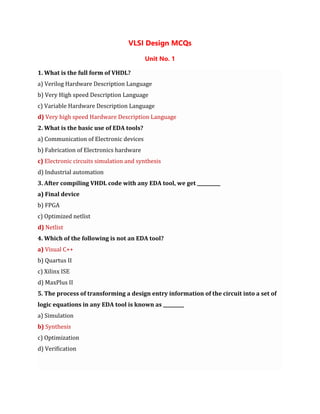
  • 1. VLSI Design MCQs Unit No. 1 1. What is the full form of VHDL? a) Verilog Hardware Description Language b) Very High speed Description Language c) Variable Hardware Description Language d) Very high speed Hardware Description Language 2. What is the basic use of EDA tools? a) Communication of Electronic devices b) Fabrication of Electronics hardware c) Electronic circuits simulation and synthesis d) Industrial automation 3. After compiling VHDL code with any EDA tool, we get __________ a) Final device b) FPGA c) Optimized netlist d) Netlist 4. Which of the following is not an EDA tool? a) Visual C++ b) Quartus II c) Xilinx ISE d) MaxPlus II 5. The process of transforming a design entry information of the circuit into a set of logic equations in any EDA tool is known as _________ a) Simulation b) Synthesis c) Optimization d) Verification
  • 2. 6. Place and Route EDA tools are used to take the design netlist and implement the design in the device. a) True b) False 7. Which of the following is not a back end EDA tool? a) Floor planning tools b) Placement tools c) Routing tools d) Simulators 8. Difference between simulation tools and Synthesis tool is _________ a) Simulators are used to check the performance of circuit and Synthesis tools are for the fabrication of circuits b) Simulators and Synthesis tools works exactly same c) Simulators are used just to check basic functionality of the circuit and Synthesis tools includes timing constraints and other factors along with simulation d) Simulation finds the error in the code and Synthesis tool corrects the code 9. What is the extension of the Netlist file; input to the place and route EDA tools? a) EIDF b) SDF c) TXT d) CPP 10. Which of the following is the basic building block of a design? a) Architecture b) Entity c) Process d) Package
  • 3. 11. A package in VHDL consists of _________ a) Commonly used architectures b) Commonly used tools c) Commonly used data types and subroutines d) Commonly used syntax and variables 12. Complete description of the circuit to be designed is given in _________ a) Architecture b) Entity c) Library d) Configurations 13. An entity can have more than one architecture. a) True b) False 14. Predefined data for an VHDL object is called ________ a) Generic b) Constant c) Attribute d) Library 15. A process is the basic unit of execution in VHDL. a) True b) False 16. Which of the following describes the structure of VHDL code correctly? a) Library Declaration; Entity Declaration; Architecture Declaration; Configurations b) Entity Declaration; Configuration; Library Declaration; Architecture Declaration c) Configuration; Library Declaration; Entity Declaration; Architecture Declaration d) Library Declaration; Configuration; Entity Declaration; Architecture Declaration
  • 4. 17. Which of the following statement is true? a) Package is a collection of Libraries b) Library is a collection of Packages c) Entity is a collection of Packages d) Architecture is a collection of Entities 18. What does modeling type refer to? a) Type of ports in entity block of VHDL code b) Type of description statements in architecture block of VHDL code c) Type of data objects d) Type of Signals 19. Which of the following is not a type of VHDL modeling? a) Behavioral modeling b) Dataflow modeling c) Structural modeling d) Component modeling 20. In behavioral modeling, what do descriptive statements describe? a) How the system performs on given input values b) How the design is to be implemented c) Netlist d) Concurrent execution 21. Which of the following statement is used in structural modeling? a) portmap b) process c) if-else d) case 22. What is the basic unit of behavioral description? a) Structure b) Sequence c) Process d) Dataflow
  • 5. 23. Which of the following modeling style follows the sequential processing of instructions? a) Dataflow modeling b) Behavior modeling c) Structural modeling d) Component modeling 24. ______modeling uses logic gates and basic blocks to describe the functionality of system. a) Behavioral b) Structural c) Dataflow d) Component Unit No. 2 1. Which sequential circuits generate the feedback path due to the cross-coupled connection from output of one gate to the input of another gate? a) Synchronous b) Asynchronous c) Both d) None of the above 2. What is/are the crucial function/s of memory elements used in the sequential circuits? a) Storage of binary information b) Specify the state of sequential c) Both a & b d) None of the above
  • 6. 3. How are the sequential circuits specified in terms of time sequence? a) By Inputs b) By Outputs c) By Internal states d) All of the above 4. The behavior of synchronous sequential circuit can be predicted by defining the signals at ______. a) discrete instants of time b) continuous instants of time c) sampling instants of time d) at any instant of time 5. Which memory elements are utilized in an asynchronous & clocked sequential circuits respectively? a) Time- delay devices & registers b) Time- delay devices & flip-flops c) Time- delay devices & counters d) Time-delay devices & latches 6. Why do the D-flipflops receives its designation or nomenclature as 'Data Flipflops' a) Due to its capability to receive data from fliflop b) Due to its capability to store data in flipflop c) Due to its capability to transfer the data into flipflop d) All of the above 7. The characteristic equation of D-flipflop implies that _____. a) the next state is dependent on previous state b) the next state is dependent on present state c) the next state is independent of previous state d) the next state is independent of present state 8. Which circuit is generated from D-flipflop due to addition of an inverter by causing reduction in the number of inputs? a) Gated JK- latch b) Gated SR- latch c) Gated T- latch d) Gated D- latch
  • 7. 9. According to Moore circuit, the output of synchronous sequential circuit depend/s on ______ of flip flop a) Past state b) Present state c) Next state d) External inputs 10. Which type of memory elements are used in synchronous sequential circuits? a) Clocked Flip flops b) Unclocked Flip flops c) Time Delay Elements d) All of the above Unit No. 3 1. Which is used to control the scan path movement? a) clock signals b) input signals c) output signals d) delay signals 2. Boundary scan test is used to test a) pins b) multipliers c) boards d) wires 3. The boundary scan path is provided with a) serial input outputs pads b) parallel input pads c) parallel output pads d) buffer pads
  • 8. 4. The boundary scan path tests the a) input nodes b) output nodes c) buffer nodes d) interconnection points 5. Boundary scan method takes lesser time on test pattern generation. a) true b) false 6. The disadvantage of boundary scan method is that the fault coverage is less. a) true b) false 7. In scan/set method, __________ is used to implement a scan path a) serial registers b) storage elements c) parallel registers d) separate register
  • 9. Unit No. 4 1. nMOS devices are formed in a) p-type substrate of high doping level b) n-type substrate of low doping level c) p-type substrate of moderate doping level d) n-type substrate of high doping level 2. Source and drain in nMOS device are isolated by a) a single diode b) two diodes c) three diodes d) four diodes 3. In depletion mode, source and drain are connected by a) insulating channel b) conducing channel c) Vdd d) Vss 4. The condition for non saturated region is a) Vds = Vgs – Vt b) Vgs lesser than Vt c) Vds lesser than Vgs – Vt d) Vds greater than Vgs – Vt 5. In enhancement mode, device is in _________ condition a) conducting b) non conducting c) partially conducting d) insulating
  • 10. 6. The condition for non conducting mode is a) Vds lesser than Vgs b) Vgs lesser than Vds c) Vgs = Vds = 0 d) Vgs = Vds = Vs = 0 7. nMOS is a) donor doped b) acceptor doped c) all of the mentioned d) none of the mentioned 8. MOS transistor structure is a) symmetrical b) non symmetrical c) semi symmetrical d) pseudo symmetrical 9. Inversion layer in enhancement mode consists of excess of a) holes b) electrons c) both in equal quantity d) neutral carriers 10. The condition for linear region is a) Vgs lesser than Vt b) Vgs greater than Vt c) Vds lesser than Vgs d) Vds greater than Vgs
  • 11. 11. As source drain voltage increases, channel depth a) increases b) decreases c) logarithmically increases d) exponentially increases 12. The enhancement MOSFET is a) Normally off MOSFET b) Useful as a very good constant voltage source c) Widely used because of easy in its fabrication d) Normally on MOSFET 13. The depletion N-channel MOSFET a) Can be operated as a JFET with zero gate voltage b) Can be operated as an enhancement MOSFET by applying +ve bias to gate c) Can be operated as an enhancement MOSFET by applying -ve bias to gate d) Cannot be operated as an enhancement MOSFET Unit No. 5 1. In accordance to the scaling technology, the total delay of the logic circuit depends on ______ a) The capacitor to be charged b) The voltage through which capacitance must be charged c) Available current d) All of the above 2. In CMOS circuits, which type of power dissipation occurs due to switching of transient current and charging & discharging of load capacitance? a) Static dissipation b) Dynamic dissipation c) Both a and b d) None of the above
  • 12. 3. In high noise margin (NMH), the difference in magnitude between the maximum HIGH output voltage of driving gate and the maximum HIGH voltage is recognized by the _________gate. a) Driven b) Receiving c) Both a and b d) None of the above 4. Which factor/s play/s a crucial role in determining the speed of CMOS logic gate? a) Load capacitance b) Supply voltage c) Gain factor of MOS d) All of the above 5. For complex gate design in CMOS, OR function needs to be implemented by _______ connection/s of MOS. a) Series b) Parallel c) Both series and parallel d) None of the above 6. In pull-up network, PMOS transistors of CMOS are connected in parallel with the provision of conducting path between output node & Vdd yielding _____ output. a) 1 b) 0 c) Both a and b d) None of the above
  • 13. 7. In CMOS inverter, the propagation delay of a gate is the/an _________ transition delay time for the signal during propagation from input to output especially when the signal changes its value. a) Highest b) Average c) Lowest d) None of the above 8. In enhancement MOSFET, the magnitude of output current __________ due to an increase in the magnitude of gate potentials. a) Increases b) Remains constant c) Decreases d) None of the above 9. Which type of MOSFET exhibits no current at zero gate voltage? a) Depletion MOSFET b) Enhancement MOSFET c) Both a and b d) None of the above
  • 14. Unit No. 6 1. Simple Programmable Logic Devices (SPLDs) are also regarded as ________. a) Programmable Array Logic (PAL) b) Generic Array Logic (GAL) c) Programmable Logic Array (PLA) d) All of the above 2. Which among the following is/are not suitable for in-system programming? a) EPROM b) EEPROM c) Flash d) All of the above 3. The devices which are based on fusible link or anti-fuse are _________time/s programmable. a) one b) two c) four d) infinite 4. Which programming technology/ies is/are predominantly associated with SPLDs and CPLDs? a) EPROM b) EEPROM c) FLASH d) All of the above 5. An Antifuse programming technology is predominantly associated with _____ a) SPLDs b) FPGAs c) CPLDs d) All of the above
  • 15. 6. FPGA devices are________type a) PLD b) EPROM c) SROM d) SLD 7. FPGS Stands for________ a) Field Programmable gate array b) First Programmable gate array c) Field Program gate array d) First Program gate array 8. Vertical and horizontal directions in FPGA are separated by________ a) A channel b) A line c) A strobe d) A gap ………………………………….All the Best………………………………….