DR. B. R. AMBEDKAR NATIONAL INSTITUTE OF TECHNOLOGY
JALANDHAR
TOPIC: Race around and Master Slave Flip Flop
SUBMITTED BY: Shubham Singh
1
What is Race Around Condition?
• It is the phenomenon which occurs in level triggered JK flip flop when
there is 1 at both of the input terminals.
• Race around means continuous toggling.
• If the width of clock pulse is too long compared to the propagation
delay of gate , the state of flip flop will keep on changing from 0 to 1,
1 to 0, 0 to 1 and so on and at the end of the clock pulse its state will
be uncertain.
2
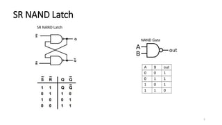
SR NAND Latch
SR NAND Latch
NAND Gate
3
4
T
JK FLIP FLOP
• The JK Flip Flop is the most widely used flip flop. It is considered
to be a universal flip-flop circuit. The sequential operation of the
JK Flip Flop is the same as for the RS flip-flop with the
same SET and RESET input.
• The difference is that the JK Flip Flop does not have invalid states
of the RS Latch (when S and R are both 1).
• The S and R inputs of the RS bistable have been replaced by the
two inputs called the J and K input respectively.
• Here J = S and K = R. The two-input AND gates of the RS flip-flop is
replaced by the two 3 inputs NAND gates with the third input of
each gate connected to the outputs at Q and Ǭ. This cross-
coupling of the RS Flip-Flop is used to produce toggle action. As
the two inputs are interlocked.
• If the circuit is in the “SET” condition, the J input is inhibited by
the status 0 of Q through the lower NAND gate. Similarly, the
input K is inhibited by 0 status of Q through the upper NAND gate
in the “RESET” condition . When both J and K are at logic “1”, the
JK Flip Flop toggle.
The circuit diagram for JK Flip
Flop is shown above
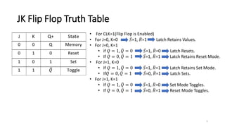
JK Flip Flop Truth Table
• For CLK=1(Flip Flop is Enabled)
• For J=0, K=0 𝑆=1, 𝑅=1 Latch Retains Values.
• For J=0, K=1
• if 𝑄 = 1, 𝑄 = 0 𝑆=1, 𝑅=0 Latch Resets.
• If 𝑄 = 0, 𝑄 = 1 𝑆=1, 𝑅=1 Latch Retains Reset Mode.
• For J=1, K=0
• If 𝑄 = 1, 𝑄 = 0 𝑆=1, 𝑅=1 Latch Retains Set Mode.
• If𝑄 = 0, 𝑄 = 1 𝑆=0, 𝑅=1 Latch Sets.
• For J=1, K=1
• If 𝑄 = 1, 𝑄 = 0 𝑆=1, 𝑅=0 Set Mode Toggles.
• If 𝑄 = 0, 𝑄 = 1 𝑆=0, 𝑅=1 Reset Mode Toggles.
5
Propagation Delay
• Propagation Delay is the average transition delay time for the signal to propagate from input to
output when the binary changes in value.
• The signal that travel through a series of gates , the sum of propagation delays through the gates is
the total propagation delay of the circuit.
6
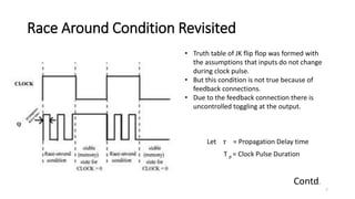
Race Around Condition Revisited
• Truth table of JK flip flop was formed with
the assumptions that inputs do not change
during clock pulse.
• But this condition is not true because of
feedback connections.
• Due to the feedback connection there is
uncontrolled toggling at the output.
Let 𝜏 = Propagation Delay time
T p = Clock Pulse Duration
Contd.
7
Race Around Condition Revisited
• For T p> N𝜏 this Racing continues. (N is natural number)
• Flip Flops keep complementing itself for every 2𝜏.
(Assumed)
Flow of Signals in Race Around Condition(J=1, K=1)
8
Solutions of Racing
1. Clock Pulse Duration≤ Propagation Delay of NAND gates (not feasible )
2. Edge triggered Flip flop
3. Master-Slave JK Flip flop
9
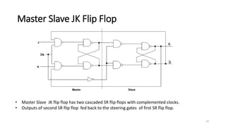
Master Slave JK Flip Flop
• Master Slave JK flip flop has two cascaded SR flip flops with complemented clocks.
• Outputs of second SR flip flop fed back to the steering gates of first SR flip flop.
10
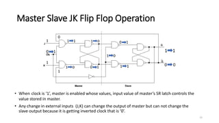
Master Slave JK Flip Flop Operation
• Assumed the output of this Master flip flop latch is 1 and 0.
• When Clock input is ‘0’ output of the inverter is ‘1’, slave latch is then enabled and its output ’Q’
is equal to the master latch output.
1
1
0 1
0
1
1 0
1
1
1
0
1
?
?
11
Master Slave JK Flip Flop Operation
• When clock is ‘1’, master is enabled whose values, input value of master’s SR latch controls the
value stored in master.
• Any change in external inputs (J,K) can change the output of master but can not change the
slave output because it is getting inverted clock that is ‘0’.
1
1
0
1
12
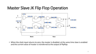
Master Slave JK Flip Flop Operation
• When the clock input returns to zero, the master is disabled, at the same time slave is enabled
and the current value of master is transferred to the output of flipflop
1
1
13
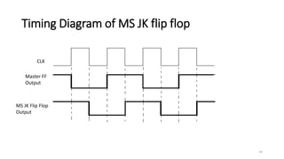
Timing Diagram of MS JK flip flop
CLK
Master FF
Output
MS JK Flip Flop
Output
14
Conclusion
We surmised that Race Around Condition in JK Flip Flop can be
eliminated in following ways:
• If the clock on or high time is less than the propagation delay of
the flip flop then racing can be avoided. This is done by using edge
triggering rather than level triggering.
• If the flip flop is made to toggle over one clock period then racing
around condition can be eliminated. This is done by using Master-
Slave JK flip-flop.
15
REFRENCES
• D. A. Godse A. P. Godse, ”Logic Design”
• Morris Mano, ’’Digital Design”
• William H. Gothman,”Digital Electronics : An Introduction To Theory
And Practice”
• A. Anand Kumar, ”Fundamentals of Digital Circuits”
16
Thank You!
17

Race around and master slave flip flop

  • 1.
    DR. B. R.AMBEDKAR NATIONAL INSTITUTE OF TECHNOLOGY JALANDHAR TOPIC: Race around and Master Slave Flip Flop SUBMITTED BY: Shubham Singh 1
  • 2.
    What is RaceAround Condition? • It is the phenomenon which occurs in level triggered JK flip flop when there is 1 at both of the input terminals. • Race around means continuous toggling. • If the width of clock pulse is too long compared to the propagation delay of gate , the state of flip flop will keep on changing from 0 to 1, 1 to 0, 0 to 1 and so on and at the end of the clock pulse its state will be uncertain. 2
  • 3.
    SR NAND Latch SRNAND Latch NAND Gate 3
  • 4.
    4 T JK FLIP FLOP •The JK Flip Flop is the most widely used flip flop. It is considered to be a universal flip-flop circuit. The sequential operation of the JK Flip Flop is the same as for the RS flip-flop with the same SET and RESET input. • The difference is that the JK Flip Flop does not have invalid states of the RS Latch (when S and R are both 1). • The S and R inputs of the RS bistable have been replaced by the two inputs called the J and K input respectively. • Here J = S and K = R. The two-input AND gates of the RS flip-flop is replaced by the two 3 inputs NAND gates with the third input of each gate connected to the outputs at Q and Ǭ. This cross- coupling of the RS Flip-Flop is used to produce toggle action. As the two inputs are interlocked. • If the circuit is in the “SET” condition, the J input is inhibited by the status 0 of Q through the lower NAND gate. Similarly, the input K is inhibited by 0 status of Q through the upper NAND gate in the “RESET” condition . When both J and K are at logic “1”, the JK Flip Flop toggle. The circuit diagram for JK Flip Flop is shown above
  • 5.
    JK Flip FlopTruth Table • For CLK=1(Flip Flop is Enabled) • For J=0, K=0 𝑆=1, 𝑅=1 Latch Retains Values. • For J=0, K=1 • if 𝑄 = 1, 𝑄 = 0 𝑆=1, 𝑅=0 Latch Resets. • If 𝑄 = 0, 𝑄 = 1 𝑆=1, 𝑅=1 Latch Retains Reset Mode. • For J=1, K=0 • If 𝑄 = 1, 𝑄 = 0 𝑆=1, 𝑅=1 Latch Retains Set Mode. • If𝑄 = 0, 𝑄 = 1 𝑆=0, 𝑅=1 Latch Sets. • For J=1, K=1 • If 𝑄 = 1, 𝑄 = 0 𝑆=1, 𝑅=0 Set Mode Toggles. • If 𝑄 = 0, 𝑄 = 1 𝑆=0, 𝑅=1 Reset Mode Toggles. 5
  • 6.
    Propagation Delay • PropagationDelay is the average transition delay time for the signal to propagate from input to output when the binary changes in value. • The signal that travel through a series of gates , the sum of propagation delays through the gates is the total propagation delay of the circuit. 6
  • 7.
    Race Around ConditionRevisited • Truth table of JK flip flop was formed with the assumptions that inputs do not change during clock pulse. • But this condition is not true because of feedback connections. • Due to the feedback connection there is uncontrolled toggling at the output. Let 𝜏 = Propagation Delay time T p = Clock Pulse Duration Contd. 7
  • 8.
    Race Around ConditionRevisited • For T p> N𝜏 this Racing continues. (N is natural number) • Flip Flops keep complementing itself for every 2𝜏. (Assumed) Flow of Signals in Race Around Condition(J=1, K=1) 8
  • 9.
    Solutions of Racing 1.Clock Pulse Duration≤ Propagation Delay of NAND gates (not feasible ) 2. Edge triggered Flip flop 3. Master-Slave JK Flip flop 9
  • 10.
    Master Slave JKFlip Flop • Master Slave JK flip flop has two cascaded SR flip flops with complemented clocks. • Outputs of second SR flip flop fed back to the steering gates of first SR flip flop. 10
  • 11.
    Master Slave JKFlip Flop Operation • Assumed the output of this Master flip flop latch is 1 and 0. • When Clock input is ‘0’ output of the inverter is ‘1’, slave latch is then enabled and its output ’Q’ is equal to the master latch output. 1 1 0 1 0 1 1 0 1 1 1 0 1 ? ? 11
  • 12.
    Master Slave JKFlip Flop Operation • When clock is ‘1’, master is enabled whose values, input value of master’s SR latch controls the value stored in master. • Any change in external inputs (J,K) can change the output of master but can not change the slave output because it is getting inverted clock that is ‘0’. 1 1 0 1 12
  • 13.
    Master Slave JKFlip Flop Operation • When the clock input returns to zero, the master is disabled, at the same time slave is enabled and the current value of master is transferred to the output of flipflop 1 1 13
  • 14.
    Timing Diagram ofMS JK flip flop CLK Master FF Output MS JK Flip Flop Output 14
  • 15.
    Conclusion We surmised thatRace Around Condition in JK Flip Flop can be eliminated in following ways: • If the clock on or high time is less than the propagation delay of the flip flop then racing can be avoided. This is done by using edge triggering rather than level triggering. • If the flip flop is made to toggle over one clock period then racing around condition can be eliminated. This is done by using Master- Slave JK flip-flop. 15
  • 16.
    REFRENCES • D. A.Godse A. P. Godse, ”Logic Design” • Morris Mano, ’’Digital Design” • William H. Gothman,”Digital Electronics : An Introduction To Theory And Practice” • A. Anand Kumar, ”Fundamentals of Digital Circuits” 16
  • 17.