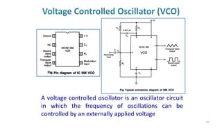
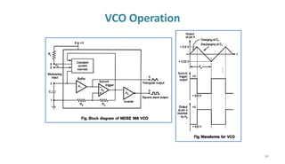
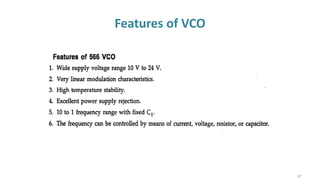
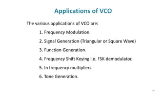
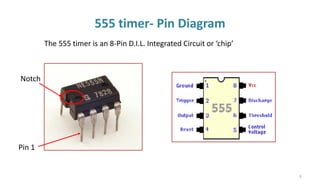
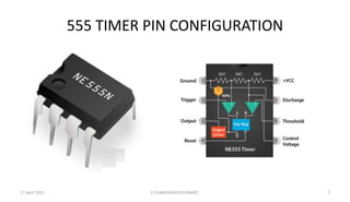
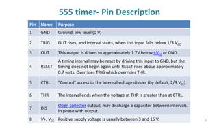
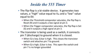
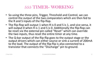
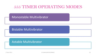
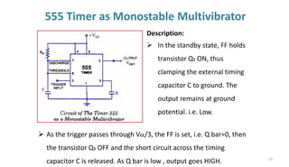
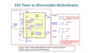
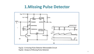
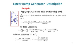
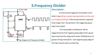
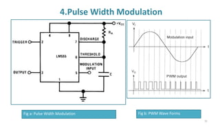
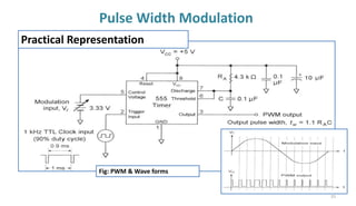
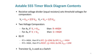
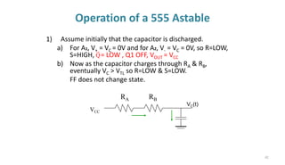
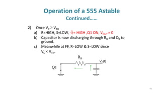
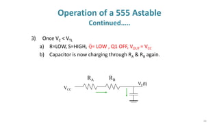
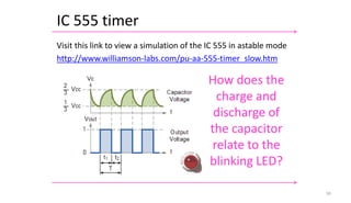
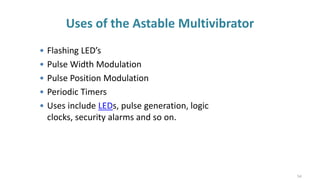
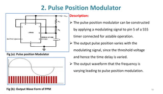
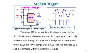
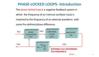
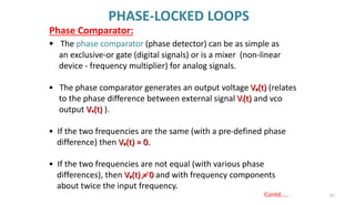
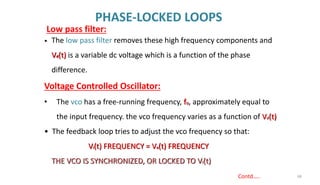
The document provides an overview of the 555 timer, a versatile integrated circuit used in various electronic applications, including timing tasks and pulse generation. It includes detailed explanations of its functional block, modes of operation (monostable, astable, and bistable), and applications, along with technical specifications and pin configurations. Additionally, the document covers related integrated circuits such as the IC-566 voltage-controlled oscillator and IC-565 phase-locked loop.

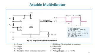
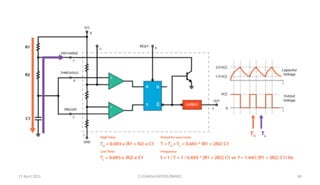
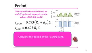
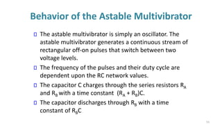
![Astable Multivibrator- Analysis
49
C
R
t B
LOW
69
.
0
=
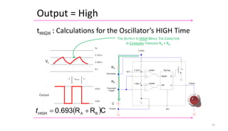
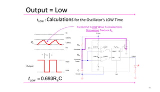
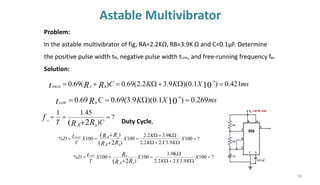
After solving, we get, t=0.69RC
For the given circuit,
Both RA and RB are in the charge path, but only RB is in the discharge path.
The total time period,
C
C
T R
R
R
t
t B
B
LOW
HIGH A 69
.
0
)
69
.
0 ( +
=
+
= +
C
C
C
C
T R
R
R
R
R
R
R
R A
A
A B
B
B
B
B
)
69
.
0
)
69
.
0
]
)
69
.
0 2
(
(
[( +
+
+ =
+
=
+
=
C
C
T
f
R
R
R
R A
A B
B
)
45
.
1
)
69
.
0
1
1
2
(
2
( +
+
=
=
=
Frequency,
Duty Cycle,
100
)
)
100
)
69
.
0
)
69
.
0
100
%
2
(
(
2
(
(
X
X
C
C
X
T
D
R
R
R
R
R
R
R
R
t
A
A
A
A
B
B
B
B
HIGH
+
+
+
+
=
=
=
100
)
100
)
69
.
0
69
.
0
100
%
2
(
2
(
X
X
C
C
X
T
D
R
R
R
R
R
R
t
A
A B
B
B
B
LOW
+
+
=
=
=
…… Discharging time
…….1.45 is Error Constant](https://image.slidesharecdn.com/licaunit4ppt-converted-210417155347/85/Lica-unit4-ppt-49-320.jpg)
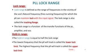
![PLL-Basic Components
74
Phase detector:
➢ Transfer function: KΦ [V/radians].
➢ Implemented as: four quad
multiplier, XOR gate, state
machine.
Voltage controlled oscillator (VCO):
➢ Frequency is the first derivative of
phase.
➢ Transfer function: KVCO/s
[radians/(V•s)]
Low pass filter:
➢ Removes high frequency components coming from the phase detector.
➢ Determines loop order and loop dynamics.](https://image.slidesharecdn.com/licaunit4ppt-converted-210417155347/85/Lica-unit4-ppt-74-320.jpg)