Ajal op amp
•Download as PPT, PDF•
7 likes•12,307 views

Understand the “magic” of negative feedback and the characteristics of ideal op amps. Understand the conditions for non-ideal op amp behavior so they can be avoided in circuit design. Demonstrate circuit analysis techniques for ideal op amps. Characterize inverting, non-inverting, summing and instrumentation amplifiers, voltage follower and first order filters. Learn the factors involved in circuit design using op amps. Find the gain characteristics of cascaded amplifiers. Special Applications: The inverted ladder DAC and successive approximation ADC

Recommended
More Related Content
What's hot
What's hot (20)
Viewers also liked
Similar to Ajal op amp
Similar to Ajal op amp (20)
More from AJAL A J
More from AJAL A J (20)
Recently uploaded
Recently uploaded (20)
Ajal op amp
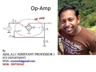
- 1. Op-Amp ByBy AJAL.A.J ( ASSISTANT PROFESSOR )AJAL.A.J ( ASSISTANT PROFESSOR ) ECE DEPARTMENTECE DEPARTMENT MAIL:MAIL: ec2reach@gmail.comec2reach@gmail.com MOB: 8907305642MOB: 8907305642
- 2. WHAT ? • An Operational Amplifier (Op-Amp) is an integrated circuit that uses external voltage to amplify the input through a very high gain. Key WordsKey Words: Op Amp Model Ideal Op Amp Op Amp transfer characteristic Feedback Virtual short
- 3. History of the Op-Amp • The Vacuum Tube Age • The First Op-Amp: (1930 – 1940) Designed by Karl Swartzel for the Bell Labs M9 gun director • Uses 3 vacuum tubes, only one input, and ± 350 V to attain a gain of 90 dB • Loebe Julie then develops an Op-Amp with
- 4. 1950’s-1960’s The end of Vacuum Tubes was built up during the 1950’s-1960’s to the advent of solid-state electronics 1.The Transistor 2.The Integrated Circuit 3.The Planar Process
- 5. 1960s: • 1960s: beginning of the Solid State Op-Amp • Example: GAP/R P45 (1961 – 1971) – Runs on ± 15 V, but costs $118 for 1 – 4 • The GAP/R PP65 (1962) makes the Op-Amp into a circuit component as a potted module
- 6. @ 1963 • The solid-state decade saw a proliferation of Op-Amps – Model 121, High Speed FET family, etc. • Robert J. Widlar develops the μA702 Monolithic IC Op- Amp (1963) and shortly after the μA709 • Fairchild Semiconductor vs. National Semiconductor – National: The LM101 (1967) and then the LM101A (1968) (both by Widlar) – Fairchild: The “famous” μA741 (by Dave Fullager 1968) and then the μA748 (1969)
- 7. Mathematics of the Op-Amp • The gain of the Op-Amp itself is calculated as: G = Vout/(V+ – V-) • The maximum output is the power supply voltage • When used in a circuit, the gain of the circuit (as opposed to the op-amp component) is: Av = Vout/Vin
- 8. Op-Amp Characteristics • Open-loop gain G is typically over 9000 • But closed-loop gain is much smaller • Rin is very large (MΩ or larger) •Rout is small (75Ω or smaller) • Effective output impedance in closed loop is very small
- 9. Ideal Op-Amp Characteristics • Open-loop gain G is infinite • Rin is infinite • Zero input current •Rout is zero
- 10. Ideal Op-Amp Analysis To analyze an op-amp feedback circuit: • Assume no current flows into either input terminal • Assume no current flows out of the output terminal • Constrain: V+ = V-
- 11. 11 Ideal Vs Practical Op-Amp Ideal Practical Open Loop gain A ∝ 105 Bandwidth BW ∝ 10-100Hz Input Impedance Zin ∝ >1MΩ Output Impedance Zout 0 Ω 10-100 Ω Output Voltage Vout Depends only on Vd = (V+−V−) Differential mode signal Depends slightly on average input Vc = (V++V−)/2 Common-Mode signal CMRR ∝ 10-100dB + − ~ AVin Vin Vout Zout=0 Ideal op-amp + − AVin Vin Vout Zout ~ Zin Practical op-amp
- 12. @ Practical opamp 3 categories are considering • 3 categories are considering Close-Loop Voltage Gain Input impedance Output impedance
- 13. Ref:080114HKN Operational Amplifier 13 Ideal Op-Amp Applications Analysis Method : Two ideal Op-Amp Properties: (1) The voltage between V+ and V− is zero V+ = V− (2) The current into both V+ and V− termainals is zero For ideal Op-Amp circuit: (1) Write the kirchhoff node equation at the noninverting terminal V+ (2) Write the kirchhoff node eqaution at the inverting terminal V− (3) Set V+ = V− and solve for the desired closed-loop gain
- 14. 2 TYPES 1. Inverting Amplifier 2. Non-Inverting Amplifier
- 15. 1. Inverting Amplifier Analysis virtual ground
- 16. 2. Non-Inverting Amplifier Analysis
- 17. 17 Op-Amp Properties (1) Infinite Open Loop gain - The gain without feedback - Equal to differential gain - Zero common-mode gain - Pratically, Gd = 20,000 to 200,000 (2) Infinite Input impedance - Input current ii ~0A - T-Ω in high-grade op-amp - m-A input current in low-grade op- amp (3) Zero Output Impedance - act as perfect internal voltage source - No internal resistance - Output impedance in series with load - Reducing output voltage to the load - Practically, Rout ~ 20-100 Ω + − V1 V2 Vo + − Vo i1~0 i2~0 + − Rout Vo' Rload outload load oload RR R VV + ′=
- 18. Op-Amp Buffer Vout = Vin Isolates loading effects A High output impedance B Low input impedance
- 20. 20 Op-Amp Differentiator RC dt dV v i o −= + − R C VoVi 0 to t1 t2 0 to t1 t2
- 23. Op-Amp Differential Amplifier If R1 = R2 and Rf = Rg:
- 24. Closed-loop gain 2 21 21 2 1 R RR v RR AR Av v IN IN o + ≈ + + = Closed-loop gain Af=vo/vin Suppose A=106 , R1=9R, R2=R, 10INo vv ≈ Gain INf vA= )1( 2 1 R R Af += Closed-loop gain: determined by resistor ratio insensitive to A, temperature
- 25. Negative feedback � )1( 2 1 R R v v A i o f +== 1 2 R R v v A i o f −== • We can adjust the closed-loop gain by changing the ratio of R2 and R1. • The closed-loop gain is (ideally) independent of op amp open-loop gain A (if A is large enough) and we can make it arbitrarily large or small and with the desired accuracy depending on the accuracy of the resistors.
- 26. � The terminal 1 is a virtual ground since terminal 2 is grounded. Inverting configuration, This is a classic example of what negative feedback does. It takes an amplifier with very large gain and through negative feedback, obtain a gain that is smaller, stable, and predictable. In effect, we have traded gain for accuracy. This kind of trade off is common in electronic circuit design… as we will see more later. Negative feedback
- 27. � Inverting configuration, Input Resistance: Assuming an ideal op amp (open-loop gain A = infinity), in the closed-loop inverting configuration, the input resistance is R1. 1 11 / R Rv v i v R i ii in === Negative feedback
- 28. 1 2 R R v v A i o f −== Inverting configuration,01 1 === o i in RR i v R We can model the closed-loop inverting amplifier (with A = infinite) with the following equivalent circuit using a voltage-controlled voltage source… Negative feedback �
- 29. 29 Frequency-Gain Relation • Ideally, signals are amplified from DC to the highest AC frequency • Practically, bandwidth is limited • 741 family op-amp have an limit bandwidth of few KHz. • Unity Gain frequency f1: the gain at unity • Cutoff frequency fc: the gain drop by 3dB from dc gain Gd (Voltage Gain) (frequency) f1 Gd 0.707Gd fc0 1 GB Product : f1 = Gd fc 20log(0.707)=3dB
- 30. 30 GB Product Example: Determine the cutoff frequency of an op-amp having a unit gain frequency f1 = 10 MHz and voltage differential gain Gd = 20V/mV Sol: Since f1 = 10 MHz By using GB production equation f1 = Gd fc fc = f1 / Gd = 10 MHz / 20 V/mV = 10 × 106 / 20 × 103 = 500 Hz (Voltage Gain) (frequency) f1 Gd 0.707Gd fc0 1 10MHz ? Hz
- 31. Op Amp transfer characteristic curve saturation )( −+ −== vvAvAv io active region
- 32. So far, we have been looking at the amplification that can be achieved for relatively small (amplitude) signals. For a fixed gain, as we increase the input signal amplitude, there is a limit to how large the output signal can be. The output saturates as it approaches the positive and negative power supply voltages. In other words, there is limited range across which the gain is linear. −+ > vv += Vvo −+ < vv −= Vvo Op Amp transfer characteristic curve
- 33. Applications of Op-Amps Filters Types: •Low pass filter •High pass filter •Band pass filter •Cascading (2 or more filters connected together) R2 + - + V0 __ + Vcc - Vcc - + R1 C Low pass filter Low pass filter Cutoff frequency Low pass filter transfer function
- 34. Applications of Op-Amps • Electrocardiogram EKG Amplification – Need to measure difference in voltage from lead 1 and lead 2 – 60 Hz interference from electrical equipment
- 35. Applications of Op-Amps • Simple EKG circuit – Uses differential amplifier to cancel common mode signal and amplify differential mode signal • Realistic EKG circuit – Uses two non-inverting amplifiers to first amplify voltage from each lead, followed by differential amplifier – Forms an “instrumentation amplifier”
- 36. Strain Gauge Use a Wheatstone bridge to determine the strain of an element by measuring the change in resistance of a strain gauge (No strain) Balanced Bridge R #1 = R #2 (Strain) Unbalanced Bridge R #1 ≠ R #2
- 37. Strain Gauge Half-Bridge Arrangement Using KCL at the inverting and non-inverting terminals of the op amp we find that ε ~ Vo = 2ΔR(Rf /R2 ) R + ΔR Rf + - + V0 __ + Vcc - Vcc - + Rf Vref R R - ΔR R Op amp used to amplify output from strain gauge
- 38. Applications of Op-Amps • Piezoelectric Transducer – Used to measure force, pressure, acceleration – Piezoelectric crystal generates an electric charge in response to deformation • Use Charge Amplifier – Just an integrator op-amp circuit
- 39. •Goal is to have VSET = VOUT •Remember that VERROR = VSET – VSENSOR •Output Process uses VERROR from the PID controller to adjust Vout such that it is ~VSET P I D Output Process Sensor VERRORVSET VOUT VSENSOR PID Controller – System Block Diagram
- 40. Applications PID Controller – System Circuit Diagram Source: http://www.ecircuitcenter.com/Circuits/op_pid/op_pid.htm Calculates VERROR = -(VSET + VSENSOR) Signal conditioning allows you to introduce a time delay which could account for things like inertia System to control -VSENSOR
- 41. Applications PID Controller – PID Controller Circuit Diagram VERR Adjust Change Kp RP1, RP2 Ki RI, CI Kd RD, CD VERR PID
- 42. Applications of Op-Amps • Example of PI Control: Temperature Control • Thermal System we wish to automatically control the temperature of: • Block Diagram of Control System:
- 43. Applications of Op-Amps • Voltage Error Circuit: • Proportiona l-Integral Control Circuit: • Example of PI Control: Temperature Control
- 44. 44 Multiple Inputs (1) Kirchhoff node equation at V+ yields, (2) Kirchhoff node equation at V− yields, (3) Setting V+ = V– yields 0=+V 0 _ = − + − + − + − −−− c c b b a a f o R VV R VV R VV R VV ∑= −= ++−= c aj j j f c c b b a a fo R V R R V R V R V RV + − Rf Va Vo Rb Ra Rc Vb Vc
- 45. Homework 1) Design a circuit to 5.0== i o f V V A 2) Find the vo=?
- 46. Review: Two fundamental Op Amp Structure Af Input voltage ( )terminal Feed back ( )terminal Inverting Amp _ _ Non inverting Amp + _