Download as PDF, PPTX
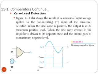
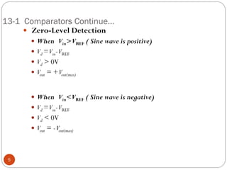
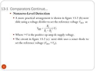
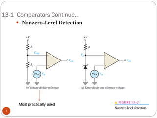
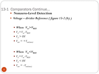
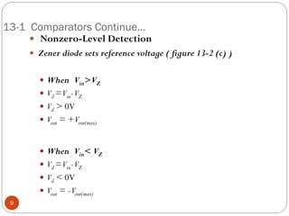
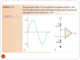
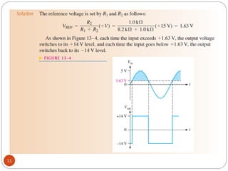
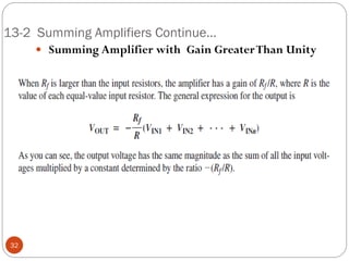
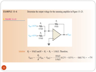
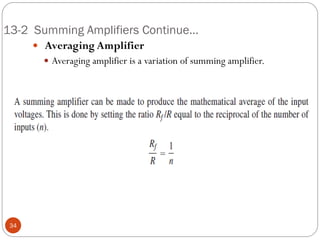
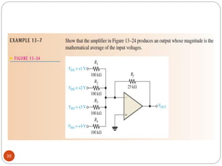
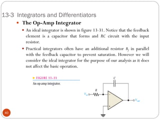
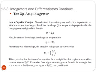
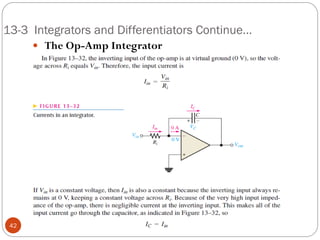
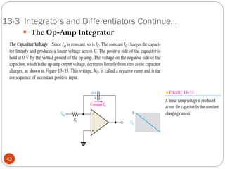
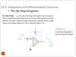
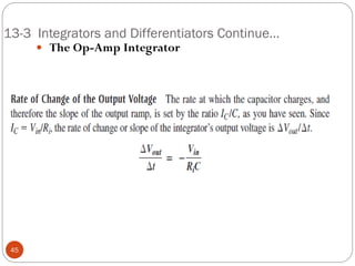
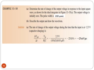
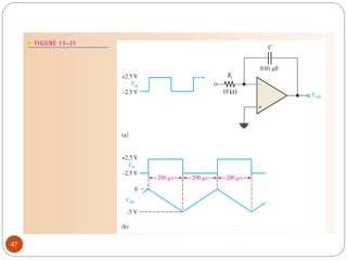

The document discusses various applications of operational amplifiers as comparators and other circuits. It describes how op-amps can be used as zero-level detectors, nonzero-level detectors, and how hysteresis can reduce noise effects in comparators. It also discusses summing amplifiers, averaging amplifiers, scaling adders, and how op-amps can be configured as integrators and differentiators.


