Download as PDF, PPTX
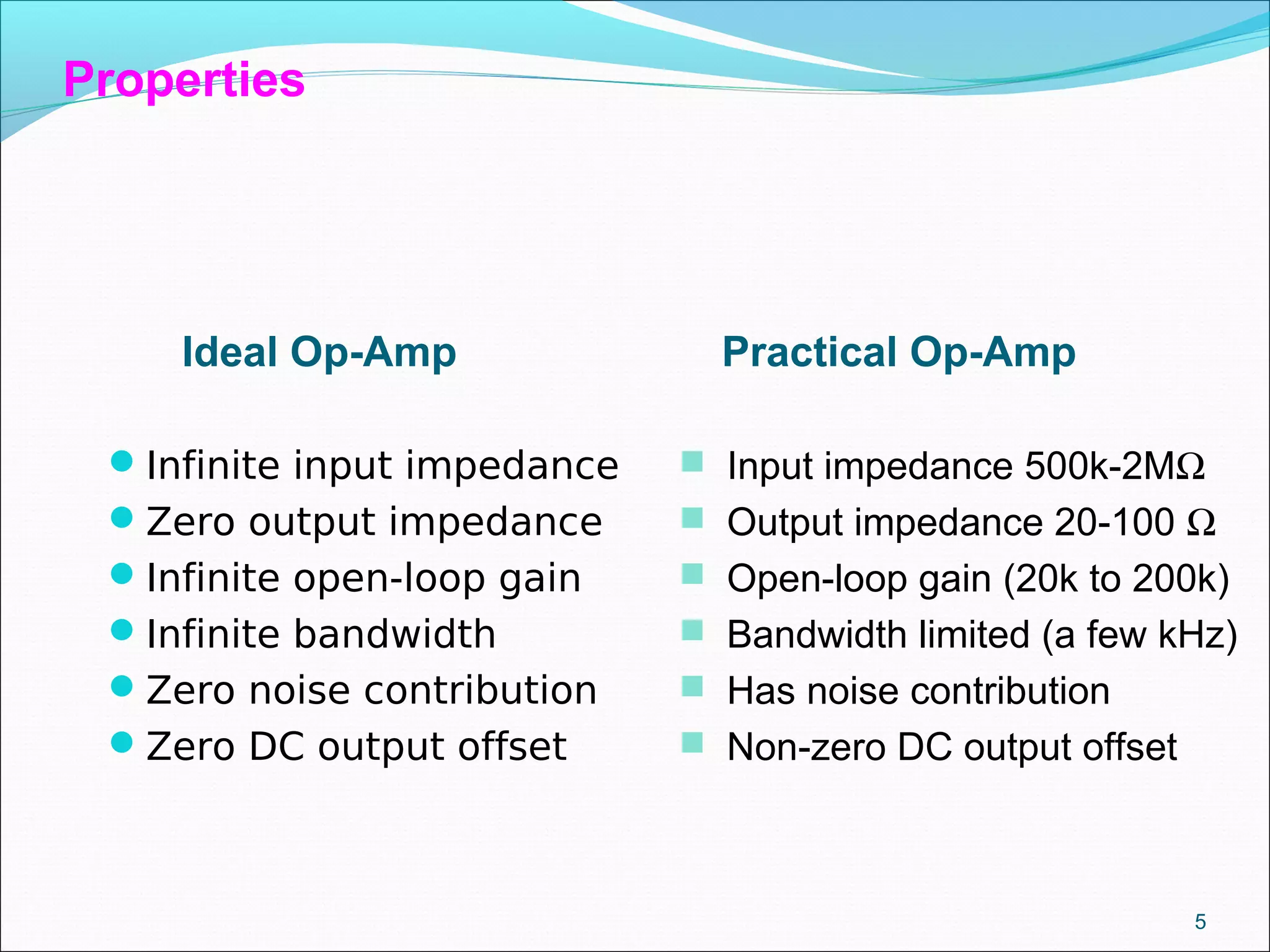
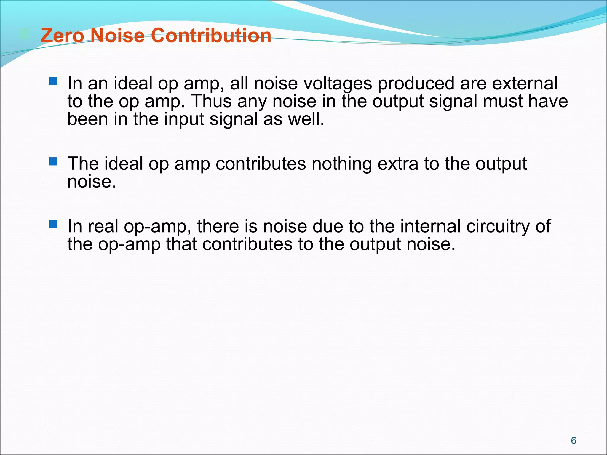

This document discusses operational amplifier (op-amp) parameters. It describes that an ideal op-amp has infinite input impedance and gain, zero output impedance and noise, and no offset voltage. However, practical op-amps have finite parameters including limited gain, nonzero output impedance and noise, and input offset voltage. It then defines and explains key op-amp parameters such as common-mode rejection ratio, input offset voltage, bias current, impedance, slew rate, and how they characterize real op-amp performance compared to ideal specifications.
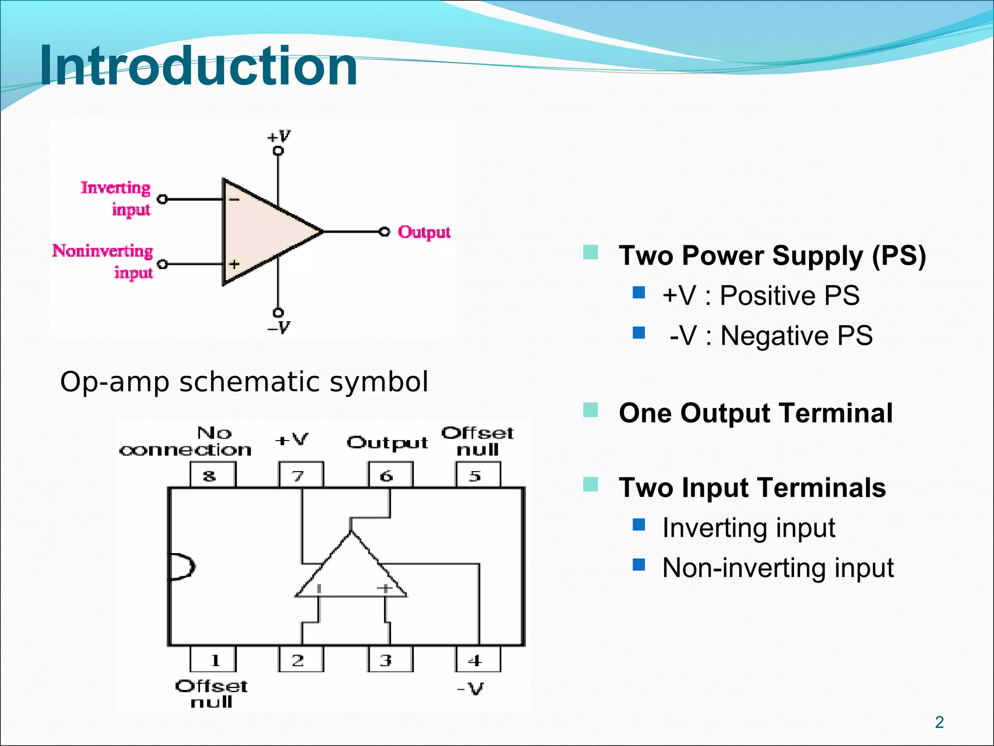
Overview of Op-amps, their symbols, and structure. Op-amps have one output, two inputs (inverting and non-inverting), and require two power supplies (+V, -V).
Op-amps are used in applications like voltage changes, comparators, oscillators, filters, sensors, and instrumentation amplifiers.
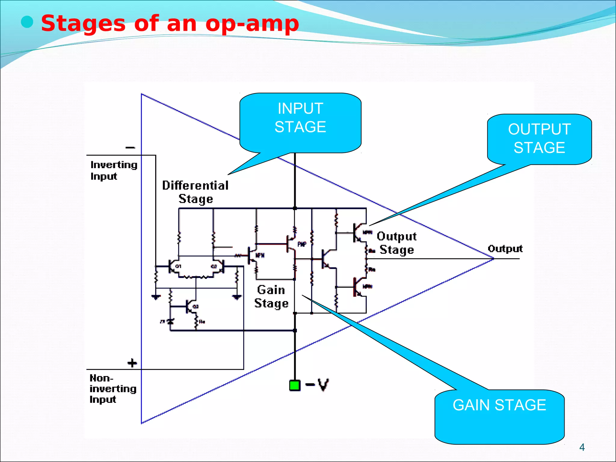
Op-amps have input, gain, and output stages. Ideal vs practical properties, including impedance, gain, bandwidth, and noise contributions.
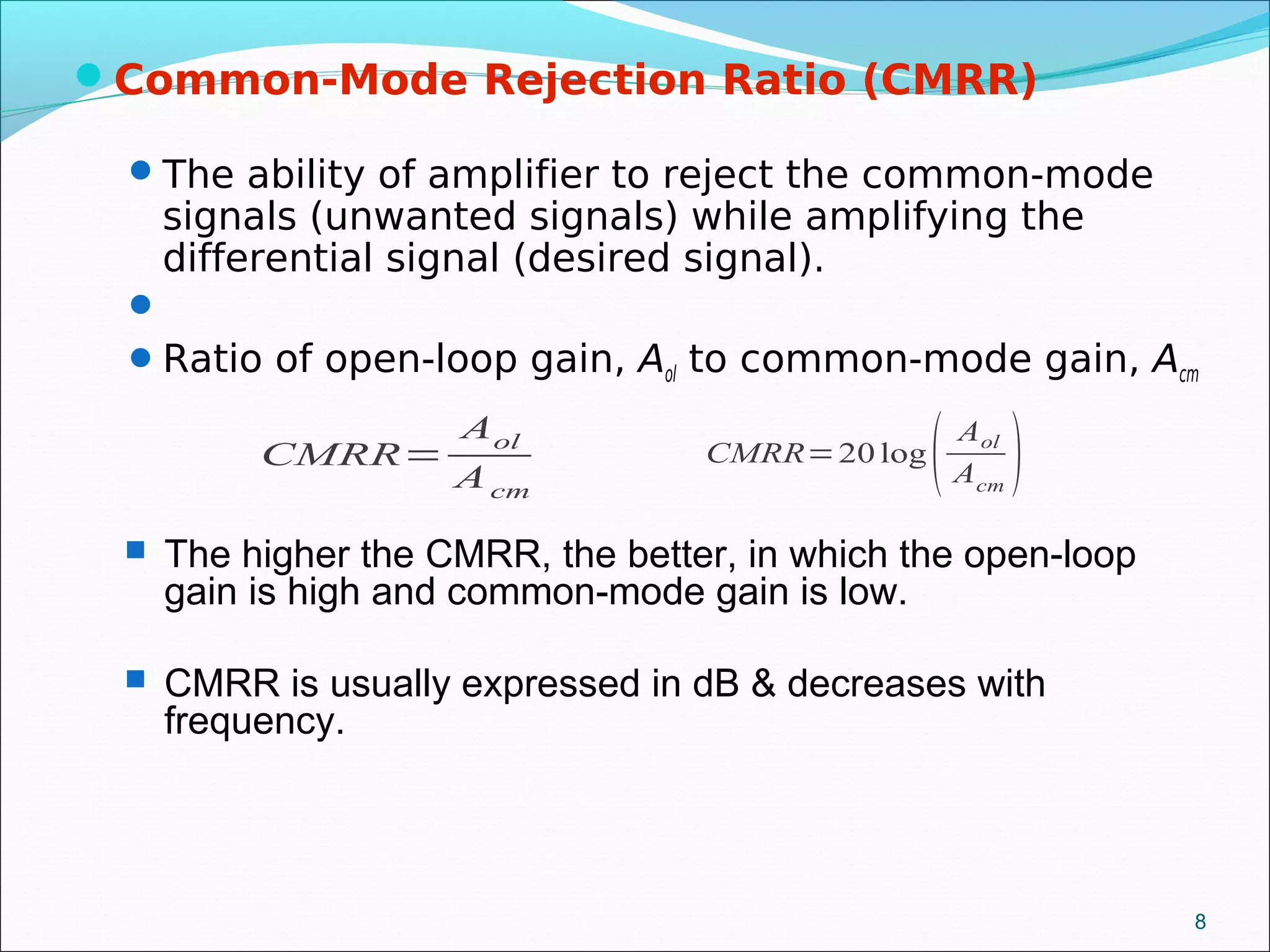
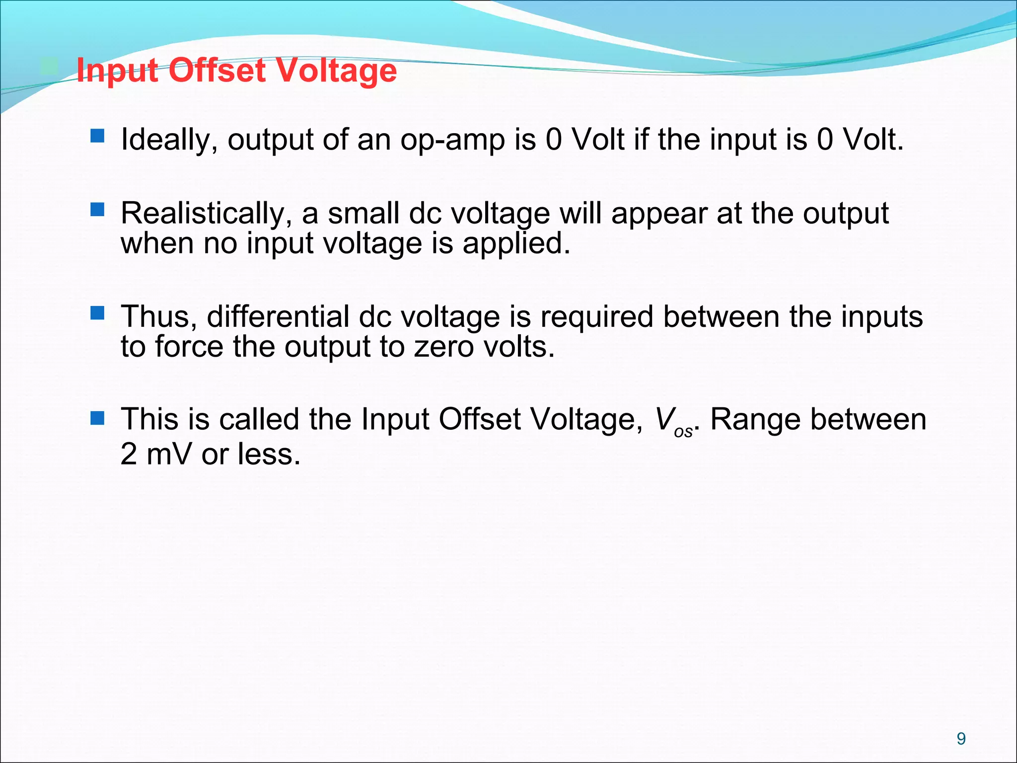
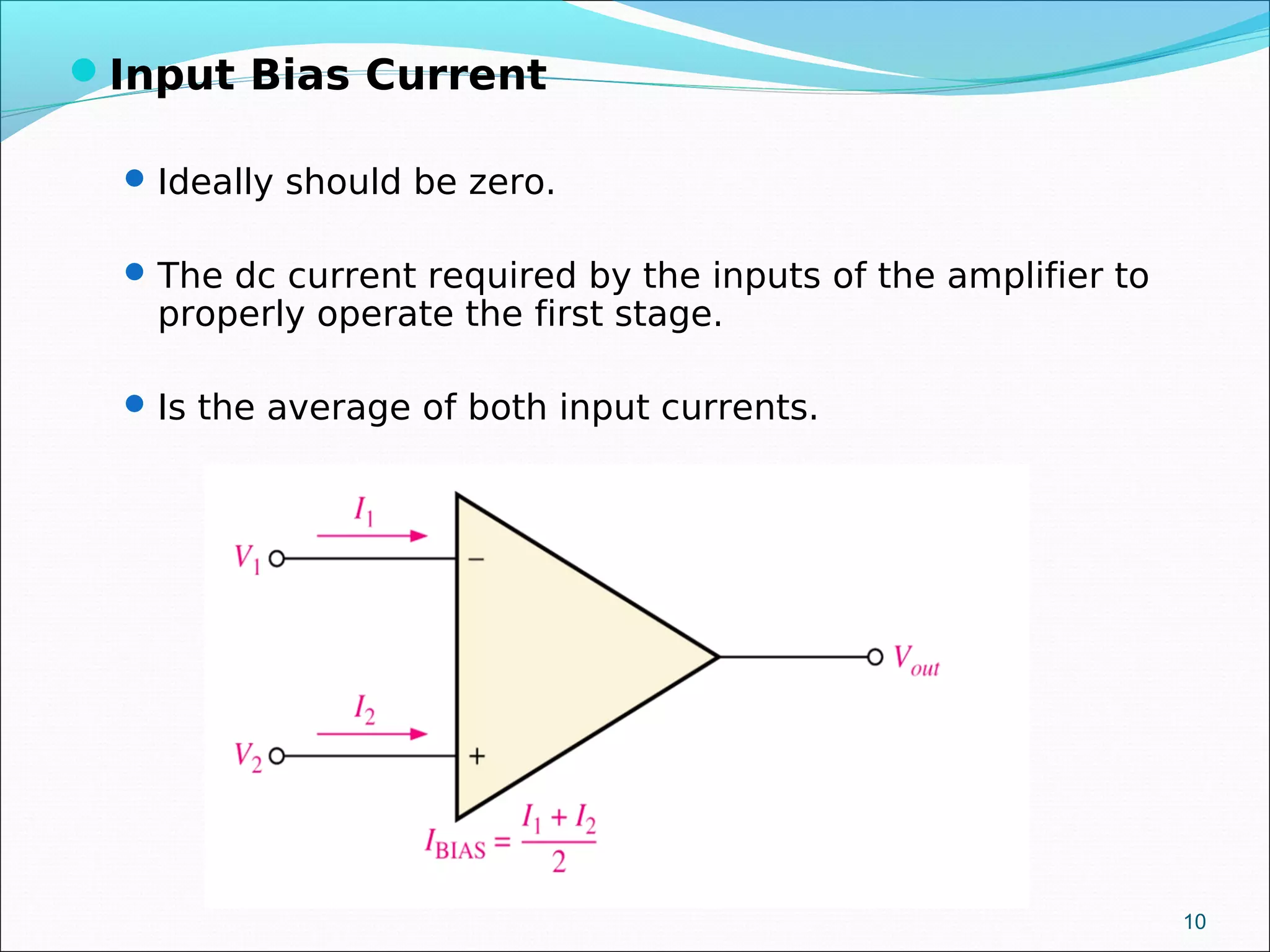
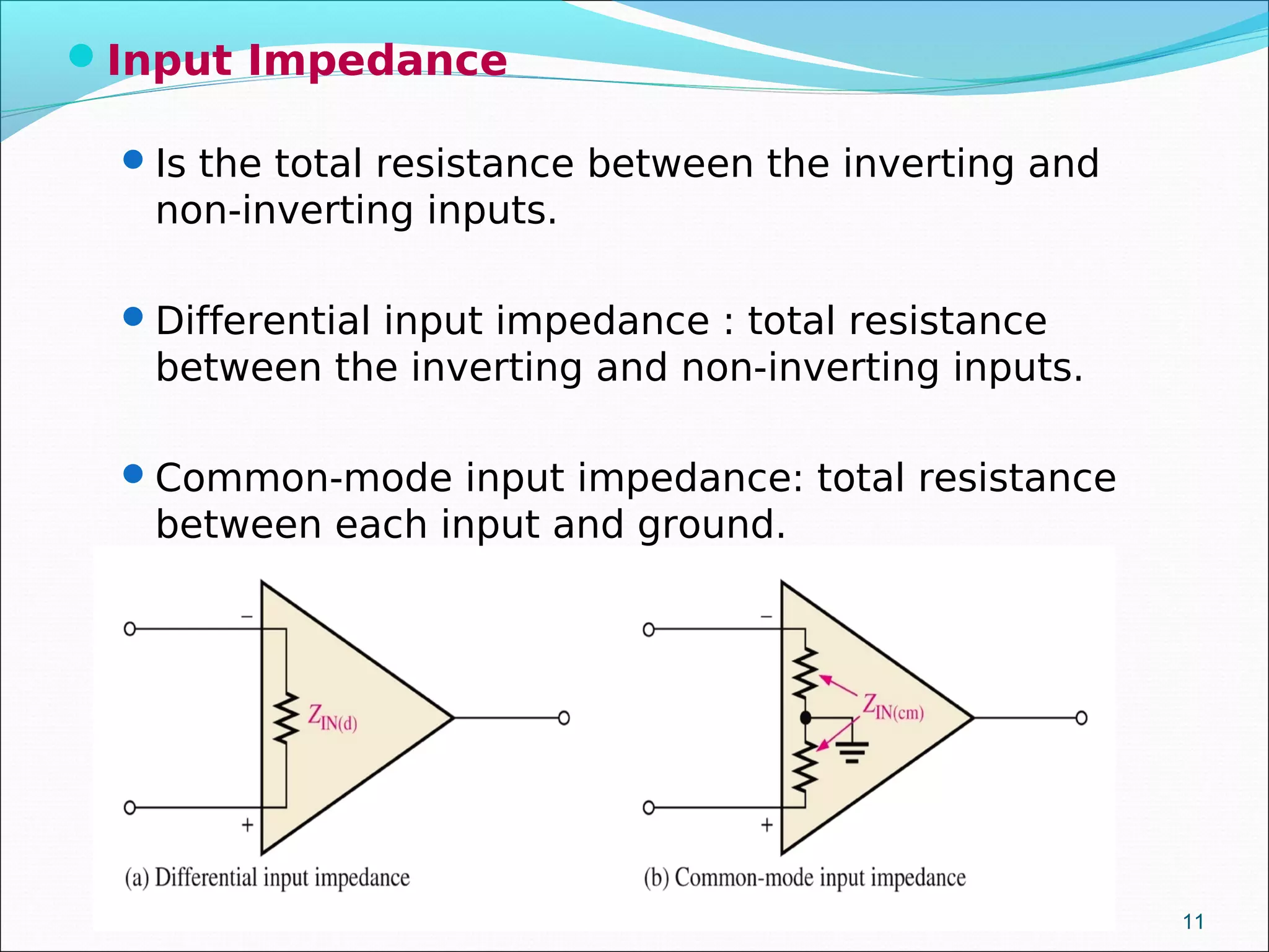
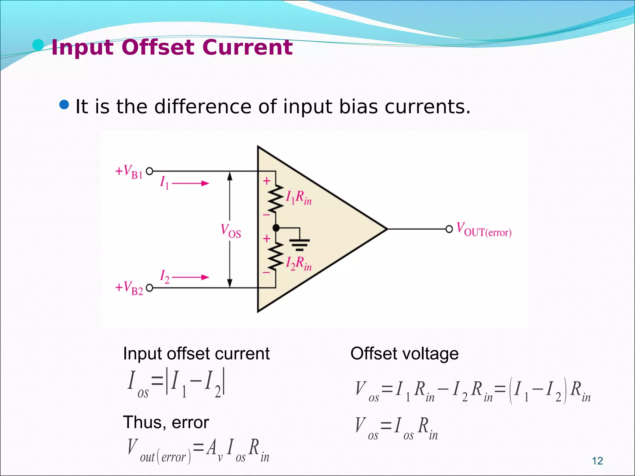
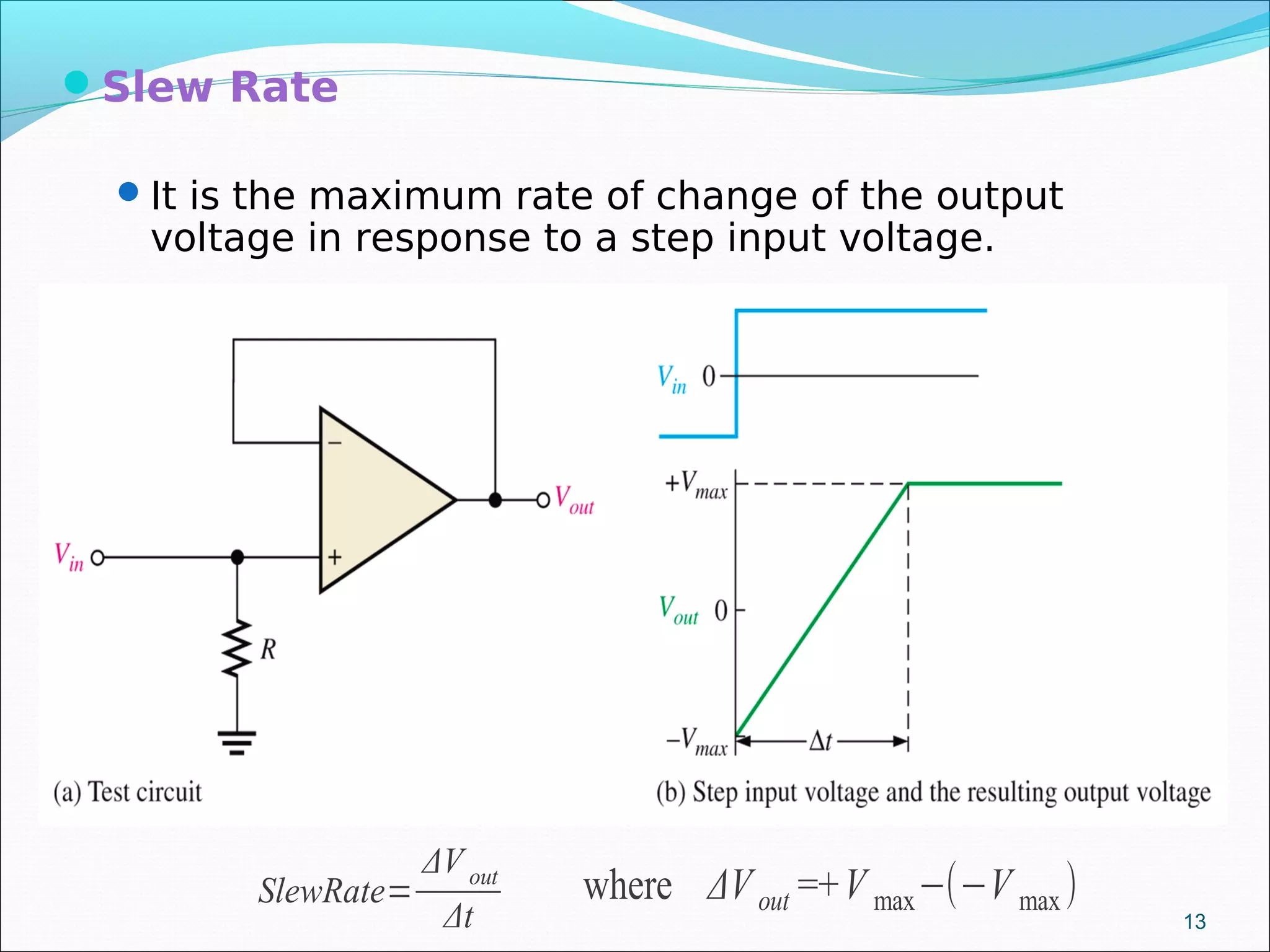
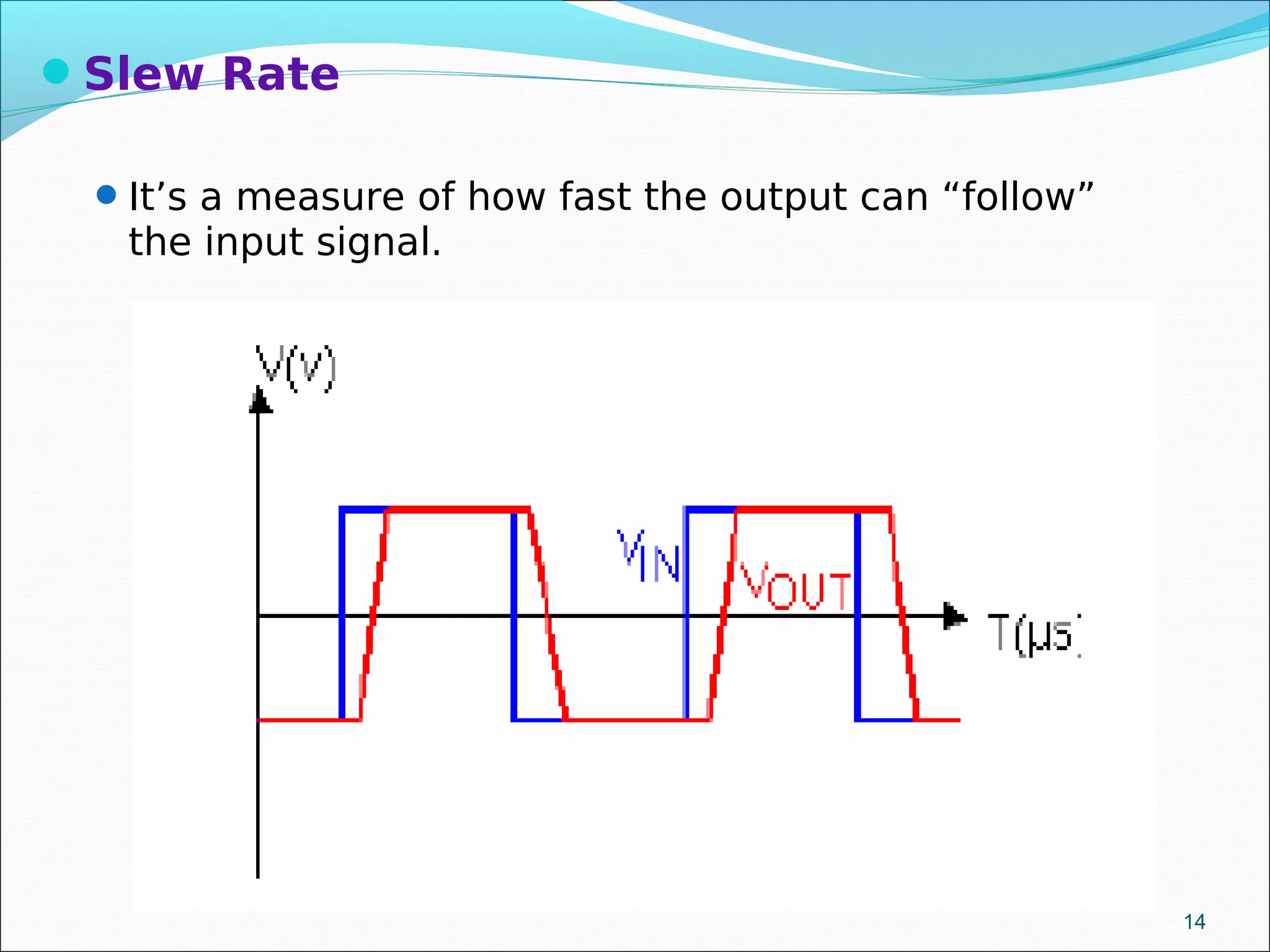
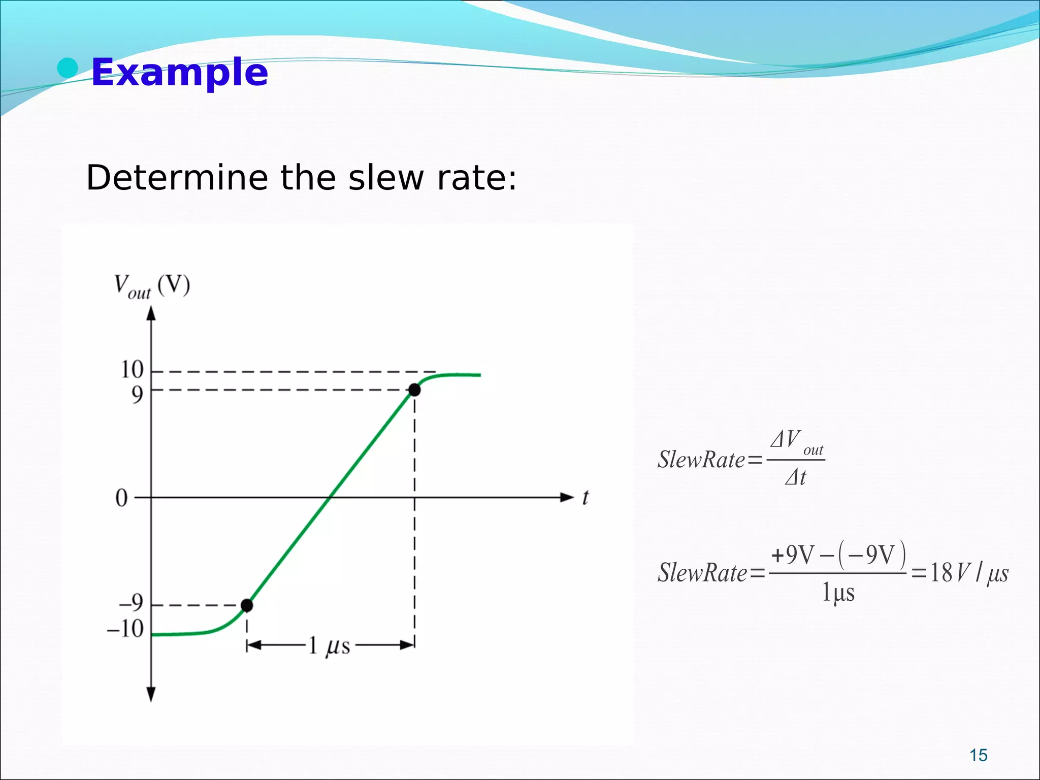
Key parameters of op-amps include CMRR, input offset voltage, input bias current, input impedance, and slew rate.Slew rate measures the speed of output voltage change. An example calculates the slew rate of a given op-amp.