Downloaded 204 times
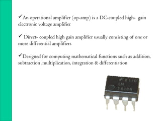
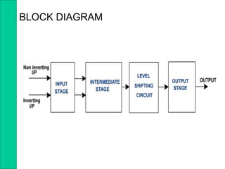
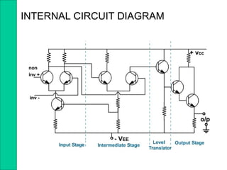
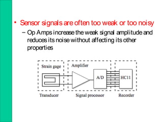

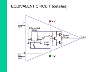
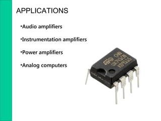
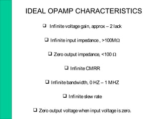


Operational amplifiers (op-amps) are high-gain electronic voltage amplifiers used for mathematical computations. They have differential inputs that amplify the difference between the voltages and provide an output proportional to that difference. Op-amps aim to have infinite gain, infinite input impedance, zero output impedance, and other ideal characteristics. They are made up of stages like input, intermediate, level shifting, and output stages. Common applications include audio amplification, instrumentation, and analog computing.