Downloaded 828 times
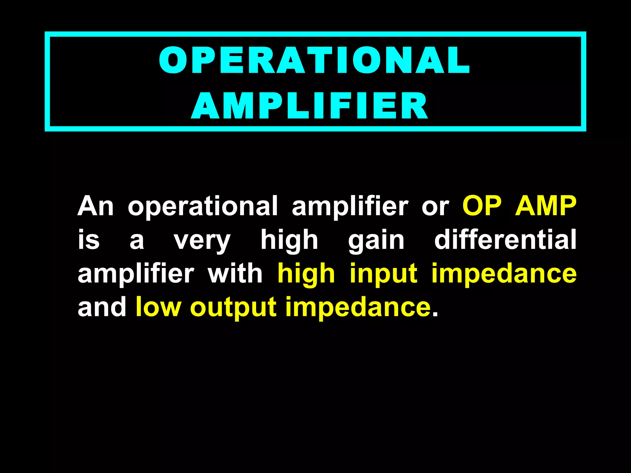
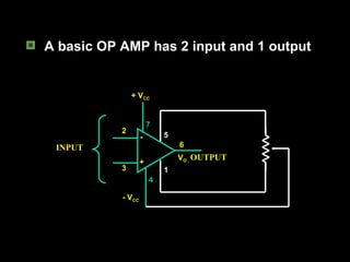

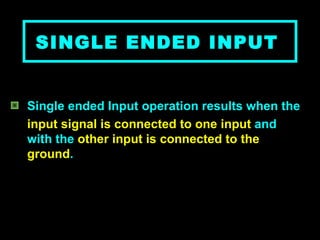
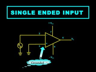

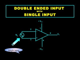
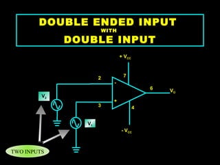
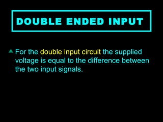
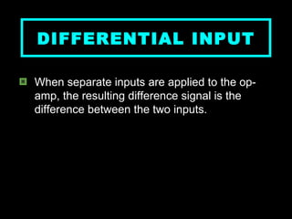
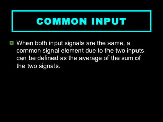
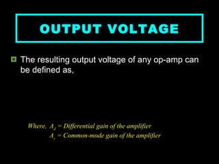


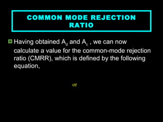
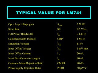

An operational amplifier, also known as an op-amp, is a high-gain differential amplifier with high input impedance and low output impedance. It has two input ports (inverting and non-inverting) and one output port. Op-amps can be used in single-ended or double-ended input configurations, with the output voltage determined by the difference or average of the input voltages multiplied by the differential or common-mode gain of the amplifier. Common applications include inverting and non-inverting amplifiers. Typical specifications for the LM741 op-amp include a voltage gain of 2 million, bandwidth of 6 kHz, and common mode rejection ratio of 90 dB.


