Downloaded 1,706 times


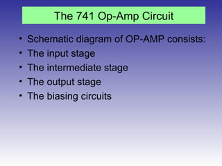
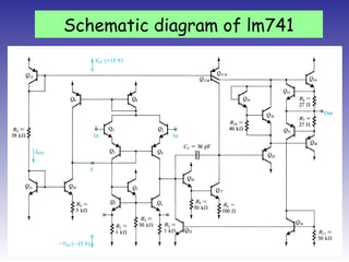
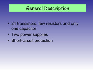
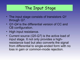
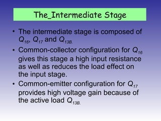
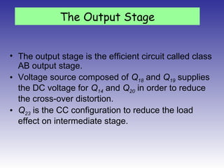
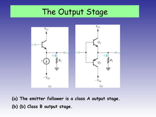
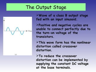
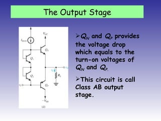
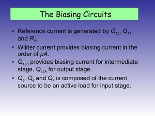

1. The op-amp circuit consists of an input stage, intermediate stage, and output stage, as well as biasing circuits. 2. The input stage uses a differential amplifier configuration to provide high input impedance. The intermediate stage provides voltage gain. 3. The output stage is typically class AB to reduce crossover distortion, using a voltage source to provide constant base voltage for the transistors.


