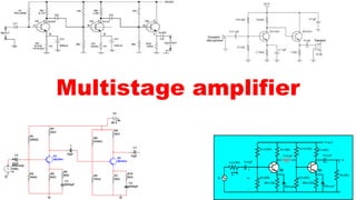
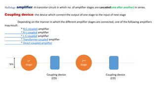
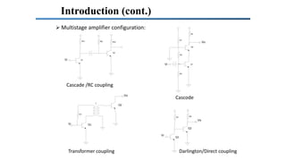
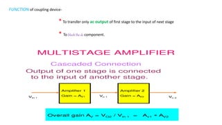
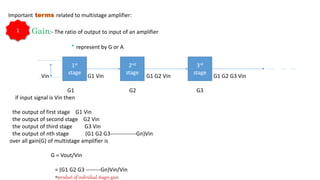
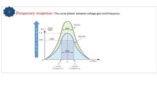
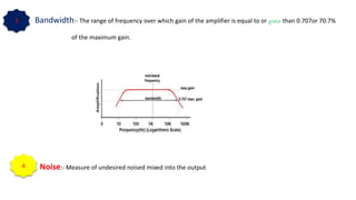
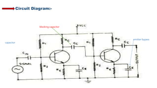
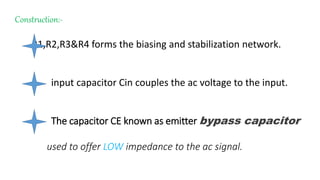
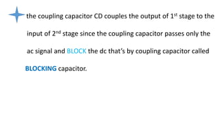
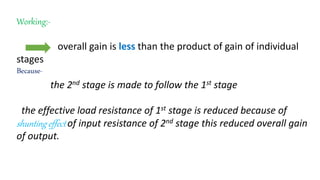
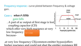
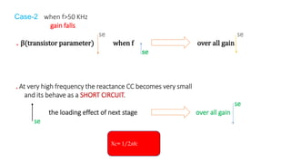
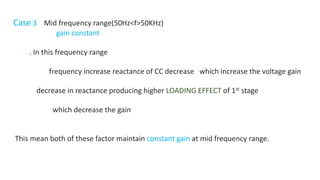
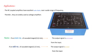
National institute of technology hamirpur
Roll no.-14240,14,55,46
Multistage amplifier
Contents:-
. Introduction
. Important terms
. Circuit diagram,working,
frequency response
. Advantages
Disadvantages
Applications
Amplifier:-A electronic device which amplifie the signals voltage&current
types of amplifier-
. Vaccume tube amplifier
. Transistor amplifier(multistage amplifier)
. Operational amplifier(op-amp)
. Video amplifier
. Fully differential amplifier
Multistage amplifier:-A transistor circuit in which no. of amplifier stages are cascaded(one after another) in series.
Coupling device:-the device which connect the output of one stage to the input of next stage
Depending on the manner in which the different amplifier stages are connected, one of the following amplifiers
may result:
* R-C coupled amplifier
* R-L coupled amplifier
* L-C coupled amplifier
* Transformer coupled amplifier
* Direct coupled amplifier
Vin
Coupling device Coupling device
(CD) (CD)
1st
stage
2nd
stage
Introduction (cont.)
 Multistage amplifier configuration:
Rc1 Rc2RB
Vi Q1
Q2
R2
RL
R1
Vo
Vi Q1
Q2
R3
R1 R2
Vi
Vo
R1
Vi
Vo
T
Cascade /RC coupling
Cascode
Transformer coupling Darlington/Direct coupling
Q1
Q2
Q1
Q2
FUNCTION of coupling device-
* To transfer only ac output of first stage to the input of next stage
* To block the dc component.
Important terms related to multistage amplifier:
Gain:- The ratio of output to input of an amplifier
* represent by G or A
Vin G1 Vin G1 G2 Vin G1 G2 G3 Vin
G1 G2 G3
if input signal is Vin then
the output of first stage G1 Vin
the output of second stage G2 Vin
the output of third stage G3 Vin
the output of nth stage (G1 G2 G3--------------Gn)Vin
over all gain(G) of multistage amplifier is
G = Vout/Vin
= (G1 G2 G3 --------Gn)Vin/Vin
=product of individual stages gain
1st
stage
2nd
stage
3rd
stage
1
Frequency response:- The curve ploted between voltage gain and frequency
2
v
o
l
t
a
g
e
Bandwidth:- The range of frequency over which gain of the amplifier is equal to or grater than 0.707or 70.7%
of the maximum gain.
Noise:- Measure of undesired noised mixed into the output
3
4
Circuit Diagram:-
blocking capacitor
emitter bypass
capacitor
Construction:-
R1,R2,R3&R4 forms the biasing and stabilization network.
input capacitor Cin couples the ac voltage to the input.
The capacitor CE known as emitter bypass capacitor
used to offer LOW impedance to the ac signal.
the coupling capacitor CD couples the output of 1st stage to the
input of 2nd stage since the coupling capacitor passes only the
ac signal and BLOCK the dc that’s by coupling capacitor called
BLOCKING capacitor.
Working:-
overall gain is less than the product of gain of individual
stages
Because-
the 2nd stage is made to follow the 1st stage
the effective load resistance of 1st stage is reduced because of
shunting effect of input resistance of 2nd stage this reduced overall gain
of output.
Frequency response:- curve ploted between frequency & voltage
gain.
Case-1 when f˂50Hz
gain falls
. A part of ac output of first stage is lost
coupling capacitor (CD)
which offer very high reactance at very
low frequency
because-
.at very low frequency CE(common emitter bypass)offers
higher reactance and could not shut the emitter resistance RE
Xc= 1/2ᴫfc
Case-2 when f>50 KHz
gain falls
se se
. β(transistor parameter) when f over all gain
se
. At very high frequency the reactance CC becomes very small
and its behave as a SHORT CIRCUIT.
se
the loading effect of next stage over all gain
se
Xc= 1/2ᴫfc
Case-3 Mid frequency range(50Hz<f>50KHz)
gain constant
. In this frequency range
frequency increase reactance of CC decrease which increase the voltage gain
decrease in reactance producing higher LOADING EFFECT of 1st stage
which decrease the gain
This mean both of these factor maintain constant gain at mid frequency range.
Advantages:-
1. It has lower cost since it employs resistors and capacitors which are cheap.
2. It has excellent frequency response.
The gain over the audio frequency range which is the region of most important for speech ,music etc.
3. The circuit is very compact
As the modern resistors and capacitors are small and extremely light.
Disadvantages:-
1. They have the tendency to become noisy with age,
Particularly in moist climates.
2. The RC coupled amplifier have low voltage and power gain.
3. Impedance matching is poor.
because the output impedance of RC coupled amplifier is several hundred ohms ,
whenever input impedance is only a few ohms.
Hence, little power will be transferred to the speaker.
Applications:-
. The RC coupled amplifiers have excellent audio fidelity over a wide range of frequency,
Therefor , they are widely used as voltage amplifiers
Note:- If an even no. of cascaded stages(2,4,6 etc), The output signal is not inverted
from the input.
If an odd no. of cascaded stages(1,3,5 etc), The output signal is inverted
from the input.
Thank You

Multistage amplifier

  • 1.
    National institute oftechnology hamirpur Roll no.-14240,14,55,46
  • 2.
  • 3.
    Contents:- . Introduction . Importantterms . Circuit diagram,working, frequency response . Advantages Disadvantages Applications
  • 4.
    Amplifier:-A electronic devicewhich amplifie the signals voltage&current types of amplifier- . Vaccume tube amplifier . Transistor amplifier(multistage amplifier) . Operational amplifier(op-amp) . Video amplifier . Fully differential amplifier
  • 5.
    Multistage amplifier:-A transistorcircuit in which no. of amplifier stages are cascaded(one after another) in series. Coupling device:-the device which connect the output of one stage to the input of next stage Depending on the manner in which the different amplifier stages are connected, one of the following amplifiers may result: * R-C coupled amplifier * R-L coupled amplifier * L-C coupled amplifier * Transformer coupled amplifier * Direct coupled amplifier Vin Coupling device Coupling device (CD) (CD) 1st stage 2nd stage
  • 6.
    Introduction (cont.)  Multistageamplifier configuration: Rc1 Rc2RB Vi Q1 Q2 R2 RL R1 Vo Vi Q1 Q2 R3 R1 R2 Vi Vo R1 Vi Vo T Cascade /RC coupling Cascode Transformer coupling Darlington/Direct coupling Q1 Q2 Q1 Q2
  • 7.
    FUNCTION of couplingdevice- * To transfer only ac output of first stage to the input of next stage * To block the dc component.
  • 8.
    Important terms relatedto multistage amplifier: Gain:- The ratio of output to input of an amplifier * represent by G or A Vin G1 Vin G1 G2 Vin G1 G2 G3 Vin G1 G2 G3 if input signal is Vin then the output of first stage G1 Vin the output of second stage G2 Vin the output of third stage G3 Vin the output of nth stage (G1 G2 G3--------------Gn)Vin over all gain(G) of multistage amplifier is G = Vout/Vin = (G1 G2 G3 --------Gn)Vin/Vin =product of individual stages gain 1st stage 2nd stage 3rd stage 1
  • 9.
    Frequency response:- Thecurve ploted between voltage gain and frequency 2 v o l t a g e
  • 10.
    Bandwidth:- The rangeof frequency over which gain of the amplifier is equal to or grater than 0.707or 70.7% of the maximum gain. Noise:- Measure of undesired noised mixed into the output 3 4
  • 11.
  • 12.
    Construction:- R1,R2,R3&R4 forms thebiasing and stabilization network. input capacitor Cin couples the ac voltage to the input. The capacitor CE known as emitter bypass capacitor used to offer LOW impedance to the ac signal.
  • 13.
    the coupling capacitorCD couples the output of 1st stage to the input of 2nd stage since the coupling capacitor passes only the ac signal and BLOCK the dc that’s by coupling capacitor called BLOCKING capacitor.
  • 14.
    Working:- overall gain isless than the product of gain of individual stages Because- the 2nd stage is made to follow the 1st stage the effective load resistance of 1st stage is reduced because of shunting effect of input resistance of 2nd stage this reduced overall gain of output.
  • 15.
    Frequency response:- curveploted between frequency & voltage gain. Case-1 when f˂50Hz gain falls . A part of ac output of first stage is lost coupling capacitor (CD) which offer very high reactance at very low frequency because- .at very low frequency CE(common emitter bypass)offers higher reactance and could not shut the emitter resistance RE Xc= 1/2ᴫfc
  • 16.
    Case-2 when f>50KHz gain falls se se . β(transistor parameter) when f over all gain se . At very high frequency the reactance CC becomes very small and its behave as a SHORT CIRCUIT. se the loading effect of next stage over all gain se Xc= 1/2ᴫfc
  • 17.
    Case-3 Mid frequencyrange(50Hz<f>50KHz) gain constant . In this frequency range frequency increase reactance of CC decrease which increase the voltage gain decrease in reactance producing higher LOADING EFFECT of 1st stage which decrease the gain This mean both of these factor maintain constant gain at mid frequency range.
  • 18.
    Advantages:- 1. It haslower cost since it employs resistors and capacitors which are cheap. 2. It has excellent frequency response. The gain over the audio frequency range which is the region of most important for speech ,music etc. 3. The circuit is very compact As the modern resistors and capacitors are small and extremely light.
  • 19.
    Disadvantages:- 1. They havethe tendency to become noisy with age, Particularly in moist climates. 2. The RC coupled amplifier have low voltage and power gain. 3. Impedance matching is poor. because the output impedance of RC coupled amplifier is several hundred ohms , whenever input impedance is only a few ohms. Hence, little power will be transferred to the speaker.
  • 20.
    Applications:- . The RCcoupled amplifiers have excellent audio fidelity over a wide range of frequency, Therefor , they are widely used as voltage amplifiers Note:- If an even no. of cascaded stages(2,4,6 etc), The output signal is not inverted from the input. If an odd no. of cascaded stages(1,3,5 etc), The output signal is inverted from the input.
  • 21.