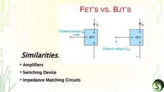
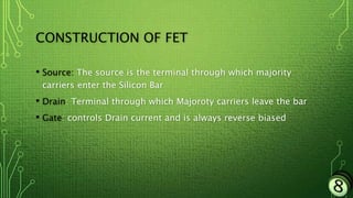
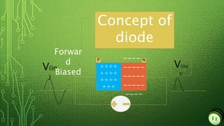
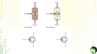
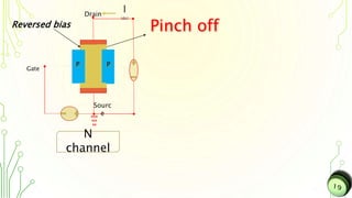
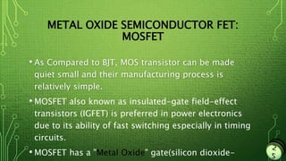
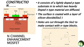
SlideShare a Scribd company logo
1 of 51
B .E Pre s e nt a t oi n
Invention
• In 1947, John Bardeen, Walter
Brattain, and William Schockly,
researchers at Bell Lab, invented
Transistor.
• They found Transistor Effect: “when
electrical contacts were applied to a
crystal of germanium, the output
power was larger than the input.”
• Awarded the Nobel Prize in physics
(1956)
• Revolutionized portability and
efficiency of electronic devices
John Bardeen, Walter
Brattain, and William
Schockly
First model of Transistor, 1947
FET
JFET
MOSFE
T
N-
channel
P-
channel
D-
MOSFET
E-
MOSFET
P-channel P-
channel
N-
channel
N-
channel
FIELD-EFFECT
TRANSISTORS
Field-effect transistors (FETs) follow
an other principle than bipolar
junction transistors
Meaning of “Field Effect” ,An electric field
is develop by the charges , this electric
field controls the conduction path of the
output ckt . So there is an effect due to
electric field and because of this reason
we call the device field effect
FETs controlled by voltage
Similarities:
• Amplifiers
• Switching Device
• Impedance Matching Circuits
DIFFERENCES
• Voltage controlled devices
• Higher input impedance
• Less sensitive to temp.
variations
• Unipolar device
• Smaller/ Easily Integrated
Chips
• Current controlled devices
• Lower impedance
• Higher sensitive
• Bipolar device
• Bigger IC
FET’s BJT’s
GENERAL OVERVIEW
• Basic Concept :
• The terminals of a FET refer to their function: Gate (G), Source
(S), Drain (D)
• FETs are voltage-controlled by the voltage between gate and
source terminal
• Voltage effects the electric field of the transistor which enlarges
or diminishes the channel
CONSTRUCTION OF FET
• Source: The source is the terminal through which majority
carriers enter the Silicon Bar
• Drain: Terminal through which Majoroty carriers leave the bar
• Gate: controls Drain current and is always reverse biased
ANALOGY OF FET WITH WATER
• The operation of FET can be compared to the water flow
through a flexible pipe
• When One end is pressed the cross sectional area decreases
hence water flow decreases
• In a FET drain is similar to outlet
• Gate is similar to control in the figure below:
++++
++++
++++
+++
-----
-----
-----
-----
----
P N
Concept of
diode
V(in
)
V(ou
t)
Forwar
d
Biased
V(in
)
V(out
)
V(in
)
V(out
)
P N
P N
Reverse
d
Biased
Reverse
d
Biased
THE
CONCLUSION
IS…….
A PN Junction with reversed biased..
Establish “depletion region”
There is no current through the junction
As the increased in voltage , the wider
the deption region.
Depletion region has no free charges.
Depletion region has fixed space.
JUNCTION FIELD-EFFECT TRANSISTORS
(JFETS)
• Simplest type of FET
• Long channel semiconductor
• Either p- or n-doped (p-type, n-type)
• A contact at each ends at source and drain terminals
• Gate terminal surrounds the channel and is doped opposite to
the doping of the channel
N PP
Gate
Source
Drain
JFET
N PP
Gate
Sourc
e
Drain
N
channel
I(ds)
v(ds)
Reversed bias
V(gs)
increased
V(GS)= 0
V(GS)=-0.5
V(GS)=-1
V(GS)=-1.5
V(GS)=-2
V(GS)=-2.5
I
(ds)
N PP
Gate
Sourc
e
Drain
N
channel
Reversed bias Pinch off
I
(ds)
if VDD is increased from 0 V, Id will increase
proportionally, as shown in the graph of Figure .In
this area, the channel resistance is essentially
constant because the depletion region is not large
enough to have significant effect. This is called
the ohmic region because VDS and ID are related
by Ohm’s law
when ID begins
to increase
very rapidly with
any
further increase
in VDS.
Breakdown can
result in
irreversible
damage to the
device, so JFETs
are always
operated below
breakdown and
within the active
• VGS Controls ID : If VGS is set to increase by adjusting
VGG . ID decreases as the magnitude of VGS is increased
to larger negative values because of the narrowing of the
channel
Regions :
 Ohmic Region – linear region
• JFET behaves like an ordinary resistor
• Saturation or Amplifier Region
• JFET operates as a constant current device because Id is relatively
independent of Vds
Breakdown Region
• If Vds is increased beyond its value corresponding to Va – avalanche
breakdown voltage.
• JFET enters the breakdown region where Id increases to an
excessive value.
Cut Off Region
• As Vgs is made more and more negative, the gate reverse bias
increases which increases the thickness of the depletion region.
• As negative value of Vgs is increased, a stage comes when the 2
depletion regions touch each other. Vgs (off) = -Vp /Vp/ =
T
METAL OXIDE SEMICONDUCTOR FET:
MOSFET
• As Compared to BJT, MOS transistor can be made
quiet small and their manufacturing process is
relatively simple.
• MOSFET also known as insulated-gate field-effect
transistors (IGFET) is preferred in power electronics
due to its ability of fast switching especially in timing
circuits.
• MOSFET has a "Metal Oxide" gate(silicon dioxide-
•This isolation of the controlling gate makes the
input resistance of the MOSFET extremely high
in the Mega-ohms region (infinite), thus
switching loss at input side can controlled and
stabilized.
•As the gate terminal is isolated from the main c
urrent carrying channel "No current flows into
the gate” so MOSFET acts as a voltage
controlled resistor (like JFET).
•MOSFET is specially used in digital
N-CHANNEL E-MOSFET SHOWING CHANNEL
LENGTH LAND CHANNEL WIDTH W
Substrate
Channel Drain
Insulator
Gate
OPERATION OF A TRANSISTOR
VSG > 0
n type operation
Positive gate bias attracts electrons into channel
Channel now becomes more conductive
More
electrons
Source
VSD
VSG
VSD
• Gate is insulated from the
body of FET so it is called
insulated gate FET(IGFET)
• Structurally there exits no
channel between source and
drain .
• Because a thin layer of P-
type substrate touching the
metal oxide film provides
channel for electrons and
hence acts like N-type
material.
N CHANNEL
ENHANCEMENT
MOSFET
MOSFET
ARCHITECTURE
• It consists of a lightly doped p type
substrate in to which two heavily
Doped n type material are diffused.
• The surface is coated with a layer of
silicon dioxide(Sio2 )
• Holes are cut through the Sio2 to
make contact with n-type blocks.
N CHANNEL
ENHANCEMENT
MOSFET
CONSTRUCTIO
N…….
WORKING OF THE ENHANCEMENT MOSFET
• Drain is made positive with
respect to the source and no
potential is applied to the gate as
shown in figure.
• The two n-blocks and p-type
substrate form back to back pn
junctions connected by the
Resistance of the p-type material.
• Both the junctions cannot be
forwarded at the Same time so
N CHANNEL
ENHANCEMENT
MOSFET
WORKING OF THE ENHANCEMENT MOSFET
• So MOSFET is cut off when
gate source voltage Is zero
• The gate is made positive
with respect to source
substrate as shown in figure
• A channel of electrons (n-
channel) is formed in
between the source and
drain regions.
N CHANNEL
ENHANCEMENT
MOSFET
• Consequently positive
charges appears on the gate
and negative charges
appears in the substrate
between the drain and
source.
• As VGS no. electrons in
the channel ID .
N CHANNEL
ENHANCEMENT
MOSFET
E-MOSFET
TRANSFER
CHARACTERISTI
C
• E-MOSFET does not have a
significant IDss parameter
• t there is ideally no drain
current until VGS reaches a
certain nonzero value
called the threshold
voltage, VGS(th).
• the curve starts at VGS(th)
rather than VGS(off)
• The equation for the E-
MOSFET transfer
characteristic curve is
OF THE E-TYPE
MOSFET
• 𝑉𝐺𝑆 is always positive
• As 𝑉𝐺𝑆 increases, 𝐼𝐷
increases
• As 𝑉𝐺𝑆 is kept constant and
𝑉𝐷𝑆 is increased, then 𝐼𝐷
saturates (𝐼𝐷𝑆𝑆 ) and the
saturation level, 𝑉𝐷𝑆𝑠𝑎𝑡 is
reached.
• 𝑉𝐷𝑆𝑠𝑎𝑡 can be calculated by
• 𝑉𝐷𝑠𝑎𝑡 = 𝑉𝐺𝑆 − 𝑉T
TRIODE REGION
A VOLTAGE-CONTROLLED RESISTOR @SMALL VDS
G
p
n+n+
metal
S DB
oxide
+-
+++
+++
- - - -
VGS1>Vt
p
n+n+
metal
S DB
oxide
+-
+++
+++
+++
- - - - - -
VGS2>VGS1
p
n+n+
metal
S DB
oxide
+-
+++
+++
+++
- - - - - - - - -
VGS3>VGS2
+++
ID
VDS
0.1 v
increasing
VGS
Increasing VGS puts more
charge in the channel, allowing
more drain current to flow
cut-off
SATURATION REGION
OCCURS AT LARGE VDS
p
n+n+
metal
source
S
gate
G
drain
D
body
B
oxide
+
-
+++
+++
+++
VDS large
As the drain voltage increases, the difference in
voltage between the drain and the gate becomes
smaller. At some point, the difference is too small
to maintain the channel near the drain  pinch-off
Saturation Region
occurs at large VDS
p
n+n+
metal
source
S
gate
G
drain
D
body
B
oxide
+
-
+++
+++
+++
VDS large
The saturation region is when the MOSFET
experiences pinch-off.
Pinch-off occurs when VG - VD is less than VT.
Saturation Region
occurs at large VDS
p
n+n+
metal
source
S
gate
G
drain
D
body
B
oxide
+
-
+++
+++
+++
VD>>Vs
VGS - VDS < VT or VGD <
VDS > VGS - VT
VT
SATURATION REGION
ONCE PINCH-OFF OCCURS, THERE IS NO
FURTHER INCREASE IN DRAIN CURRENT
ID
VDS
0.1 v
increasing
VGS
triode
saturation
VDS>VGS-VT
VDS<VGS-VT
CONSTRUCTION OF N
CHANNEL DEPLETION
MOSFET
• An n-type channel is obtained by
diffusion between N+ type
source and drain in an n-channel
MOSFET.
• In depletion MOSFET a lightly
doped n-type channel has been
introduced between to heavily
doped source& drain blocks,.
• •In depletion MOSFET a lightly
doped n-type channel has been
introduced between to heavily
doped source& drain blocks.
CONSTRUCTION OF P
CHANNEL DEPLETION
MOSFET
• An p-type channel is obtained by
diffusion between p+ type source
and drain in an p channel
MOSFET.
• In p-channel depletion MOSFETs
are made by using n-type
substrate and diffusing a lightly
doped p-type channel between
two heavily doped P-type source
& drain blocks
WORKING
• Negative gate
• When Vgs =0 electrons can flow freely from
source to drain through the conducting
channel. since a channel exists between drain &
source, Id flows even when Vgs =0
• With negative voltage a depletion MOSFET
behave like JFET.
• The action of negative voltage on gate is to
deplete the channel of free n-type charge
carriers so named as depletion MOSFET.
• The negative potential at the gate pressure
electrons toward the p -type substrate and
attract the holes for the p-type substrate
• When 𝑉𝐺𝑆 is reduced to 𝑉𝑃 (pinch off voltage),
then
N CHANNEL
DEPLETION MOSFE
DRAIN CHARACTERISTICS
• When the gate source voltage is zero
considerable drain current flows.
• When the gate is applied with negative
voltage, positive charge are induced in
the n channel through the SiO2 layer
of the gate capacitor.
• The conduction in n channel FET is due
to electrons i.e., the majority carriers
• Therefore the induced positive charges
make the n-channel less conductive.
• The voltage drop due to the drain
current causes the channel region
nearer to the drain to be more
depleted than the region due to the
The transfer characteristics are similar to the JFET
In Depletion Mode operation:
When VGS = 0V, ID = IDSS
When VGS < 0V, ID < IDSS
When VGS > 0V, ID > IDSS
The formula used to plot the Transfer Curve, is:
The transfer characteristics are similar to the JFET
In Depletion Mode operation:
When VGS = 0V, ID = IDSS
When VGS < 0V, ID < IDSS
When VGS > 0V, ID > IDSS
The formula used to plot the Transfer Curve, is:  
 
 
2
GS
D DSS
P
V
I = I 1-
V
The depletion MOSFET can also be
operated in enhancement mode
simply by applying a positive
voltage to the gate
DUAL-GATE MOSFETS
• The dual-gate MOSFET can be either a depletion or an enhancement
type.
The only difference is that it has two gates
Advantage of the dual-gate:
•Capacitance is reduced
• Used for Automatic gain control (AGC)
COMPARISON OF MOSFET AND JFET
• JFET Gate is not insulated
from the channel
• Channel and gate forms two
pn junctions
• There are only 3 leads
• Can be operated in depletion
mode only
• Input impedance is high
• MOSFET or IGFET is insulated
from the channel
• Channel and gate forms
parrallel plate capacitor.
• There are 4 leads
• Can be operated in both
depletion and enhancement
mode
• Input impedance is very high
JFET MOSFET
Summary Table

More Related Content

What's hot

Field Effect Transistor (FET)
Field Effect Transistor (FET)Field Effect Transistor (FET)
Field Effect Transistor (FET)Jess Rangcasajo
 
FIELD EFFECT TRANSISTERS (FET)
FIELD EFFECT TRANSISTERS (FET)FIELD EFFECT TRANSISTERS (FET)
FIELD EFFECT TRANSISTERS (FET)imtiazalijoono
 
Presentation on-FET( Field Effect Transistor)
Presentation on-FET( Field Effect Transistor)Presentation on-FET( Field Effect Transistor)
Presentation on-FET( Field Effect Transistor)UthsoNandy
 
BJT, FET, MOSFET as Switch
BJT, FET, MOSFET as SwitchBJT, FET, MOSFET as Switch
BJT, FET, MOSFET as SwitchParas Trivedi
 
FET lecture_Electronics by Arif Sir
FET lecture_Electronics by Arif SirFET lecture_Electronics by Arif Sir
FET lecture_Electronics by Arif SirMuntasir Mahdi
 
Presentation on bipolar junction transistor
Presentation on bipolar junction transistorPresentation on bipolar junction transistor
Presentation on bipolar junction transistorKawsar Ahmed
 
Bio-polar junction transistor (edc)
Bio-polar junction transistor  (edc)Bio-polar junction transistor  (edc)
Bio-polar junction transistor (edc)Abhinay Potlabathini
 
Types of time base generators
Types of time base generatorsTypes of time base generators
Types of time base generatorsKetki Jakatdar
 
Introduction to Junction Field Effect Transistor
Introduction to Junction Field Effect TransistorIntroduction to Junction Field Effect Transistor
Introduction to Junction Field Effect TransistorVARUN KUMAR
 
(Latest) topic 5 field_effect_transistors
(Latest) topic 5 field_effect_transistors(Latest) topic 5 field_effect_transistors
(Latest) topic 5 field_effect_transistorsGabriel O'Brien
 

What's hot (20)

Jfet electronica 2
Jfet  electronica 2Jfet  electronica 2
Jfet electronica 2
 
Field Effect Transistor (FET)
Field Effect Transistor (FET)Field Effect Transistor (FET)
Field Effect Transistor (FET)
 
FIELD EFFECT TRANSISTERS (FET)
FIELD EFFECT TRANSISTERS (FET)FIELD EFFECT TRANSISTERS (FET)
FIELD EFFECT TRANSISTERS (FET)
 
igbt and its characteristics
igbt and its characteristicsigbt and its characteristics
igbt and its characteristics
 
Presentation on-FET( Field Effect Transistor)
Presentation on-FET( Field Effect Transistor)Presentation on-FET( Field Effect Transistor)
Presentation on-FET( Field Effect Transistor)
 
Ujt relaxation oscillators
Ujt relaxation oscillatorsUjt relaxation oscillators
Ujt relaxation oscillators
 
BJT, FET, MOSFET as Switch
BJT, FET, MOSFET as SwitchBJT, FET, MOSFET as Switch
BJT, FET, MOSFET as Switch
 
JFET TRANSISTER with reference,working and conclusion
JFET TRANSISTER with reference,working and conclusionJFET TRANSISTER with reference,working and conclusion
JFET TRANSISTER with reference,working and conclusion
 
FET lecture_Electronics by Arif Sir
FET lecture_Electronics by Arif SirFET lecture_Electronics by Arif Sir
FET lecture_Electronics by Arif Sir
 
FET AMPLIFIER
FET AMPLIFIERFET AMPLIFIER
FET AMPLIFIER
 
Presentation on bipolar junction transistor
Presentation on bipolar junction transistorPresentation on bipolar junction transistor
Presentation on bipolar junction transistor
 
Bio-polar junction transistor (edc)
Bio-polar junction transistor  (edc)Bio-polar junction transistor  (edc)
Bio-polar junction transistor (edc)
 
Transistors
TransistorsTransistors
Transistors
 
Mosfet
MosfetMosfet
Mosfet
 
PUT (industrial electronic)
PUT (industrial electronic)PUT (industrial electronic)
PUT (industrial electronic)
 
Types of time base generators
Types of time base generatorsTypes of time base generators
Types of time base generators
 
Introduction to Junction Field Effect Transistor
Introduction to Junction Field Effect TransistorIntroduction to Junction Field Effect Transistor
Introduction to Junction Field Effect Transistor
 
Transistor as a switch
Transistor as a switch Transistor as a switch
Transistor as a switch
 
Mosfet
MosfetMosfet
Mosfet
 
(Latest) topic 5 field_effect_transistors
(Latest) topic 5 field_effect_transistors(Latest) topic 5 field_effect_transistors
(Latest) topic 5 field_effect_transistors
 

Viewers also liked (20)

Power control devices
Power control devicesPower control devices
Power control devices
 
Solenoid
Solenoid Solenoid
Solenoid
 
Solenoid
SolenoidSolenoid
Solenoid
 
Triac and diac
Triac and diacTriac and diac
Triac and diac
 
Solenoid
SolenoidSolenoid
Solenoid
 
Solenoids
SolenoidsSolenoids
Solenoids
 
Actuators
ActuatorsActuators
Actuators
 
Triac (industrial electronic)
Triac (industrial electronic)Triac (industrial electronic)
Triac (industrial electronic)
 
thyristors
 thyristors thyristors
thyristors
 
Different types of transistors and their functions
Different types of transistors and their functionsDifferent types of transistors and their functions
Different types of transistors and their functions
 
CBSE XII Boolean Algebra
CBSE XII Boolean AlgebraCBSE XII Boolean Algebra
CBSE XII Boolean Algebra
 
Presentation on solenoid valve
Presentation on solenoid valvePresentation on solenoid valve
Presentation on solenoid valve
 
Thyristors
ThyristorsThyristors
Thyristors
 
Power electronics 12. application devices
Power electronics   12. application devicesPower electronics   12. application devices
Power electronics 12. application devices
 
MOSFET Discription Presentation
MOSFET Discription PresentationMOSFET Discription Presentation
MOSFET Discription Presentation
 
DAC-digital to analog converter
DAC-digital to analog converterDAC-digital to analog converter
DAC-digital to analog converter
 
Induction motor
Induction motorInduction motor
Induction motor
 
Actuators
ActuatorsActuators
Actuators
 
Dc motor
Dc motorDc motor
Dc motor
 
Brushless DC Motors
Brushless DC MotorsBrushless DC Motors
Brushless DC Motors
 

Similar to FET (20)

MOSFET.pptx
MOSFET.pptxMOSFET.pptx
MOSFET.pptx
 
JFET.pptx
JFET.pptxJFET.pptx
JFET.pptx
 
MODULE 2 FET.pptx
MODULE 2 FET.pptxMODULE 2 FET.pptx
MODULE 2 FET.pptx
 
PPT ON FET OF BASIC ELECTRICAL ENGG. DIPLOMA
PPT ON FET OF BASIC ELECTRICAL ENGG. DIPLOMAPPT ON FET OF BASIC ELECTRICAL ENGG. DIPLOMA
PPT ON FET OF BASIC ELECTRICAL ENGG. DIPLOMA
 
Field effect transistors and MOSFET's
Field effect transistors and MOSFET'sField effect transistors and MOSFET's
Field effect transistors and MOSFET's
 
Mosfet Operation and Charecteristics.
Mosfet Operation and Charecteristics.Mosfet Operation and Charecteristics.
Mosfet Operation and Charecteristics.
 
5 transistor applications
5 transistor applications5 transistor applications
5 transistor applications
 
FET..pptx
FET..pptxFET..pptx
FET..pptx
 
Mosfet
MosfetMosfet
Mosfet
 
Mosfet
MosfetMosfet
Mosfet
 
Assignment
AssignmentAssignment
Assignment
 
Parulfinal
ParulfinalParulfinal
Parulfinal
 
FET.pptx
FET.pptxFET.pptx
FET.pptx
 
Basics of JFET
Basics of JFETBasics of JFET
Basics of JFET
 
Field Effect Transistor ppt
Field Effect Transistor pptField Effect Transistor ppt
Field Effect Transistor ppt
 
Mosfet
MosfetMosfet
Mosfet
 
Edcqnaunit 6
Edcqnaunit 6Edcqnaunit 6
Edcqnaunit 6
 
MOS transistor 13
MOS transistor 13MOS transistor 13
MOS transistor 13
 
Electronics 1 : Chapter # 08 : Field effect transistor
Electronics 1 : Chapter # 08 : Field effect transistorElectronics 1 : Chapter # 08 : Field effect transistor
Electronics 1 : Chapter # 08 : Field effect transistor
 
Lightly Doped Drain
Lightly Doped DrainLightly Doped Drain
Lightly Doped Drain
 

Recently uploaded

IVE Industry Focused Event - Defence Sector 2024
IVE Industry Focused Event - Defence Sector 2024IVE Industry Focused Event - Defence Sector 2024
IVE Industry Focused Event - Defence Sector 2024Mark Billinghurst
 
Call Girls Narol 7397865700 Independent Call Girls
Call Girls Narol 7397865700 Independent Call GirlsCall Girls Narol 7397865700 Independent Call Girls
Call Girls Narol 7397865700 Independent Call Girlsssuser7cb4ff
 
Study on Air-Water & Water-Water Heat Exchange in a Finned Tube Exchanger
Study on Air-Water & Water-Water Heat Exchange in a Finned Tube ExchangerStudy on Air-Water & Water-Water Heat Exchange in a Finned Tube Exchanger
Study on Air-Water & Water-Water Heat Exchange in a Finned Tube ExchangerAnamika Sarkar
 
Heart Disease Prediction using machine learning.pptx
Heart Disease Prediction using machine learning.pptxHeart Disease Prediction using machine learning.pptx
Heart Disease Prediction using machine learning.pptxPoojaBan
 
Artificial-Intelligence-in-Electronics (K).pptx
Artificial-Intelligence-in-Electronics (K).pptxArtificial-Intelligence-in-Electronics (K).pptx
Artificial-Intelligence-in-Electronics (K).pptxbritheesh05
 
CCS355 Neural Network & Deep Learning Unit II Notes with Question bank .pdf
CCS355 Neural Network & Deep Learning Unit II Notes with Question bank .pdfCCS355 Neural Network & Deep Learning Unit II Notes with Question bank .pdf
CCS355 Neural Network & Deep Learning Unit II Notes with Question bank .pdfAsst.prof M.Gokilavani
 
Call Us ≽ 8377877756 ≼ Call Girls In Shastri Nagar (Delhi)
Call Us ≽ 8377877756 ≼ Call Girls In Shastri Nagar (Delhi)Call Us ≽ 8377877756 ≼ Call Girls In Shastri Nagar (Delhi)
Call Us ≽ 8377877756 ≼ Call Girls In Shastri Nagar (Delhi)dollysharma2066
 
VICTOR MAESTRE RAMIREZ - Planetary Defender on NASA's Double Asteroid Redirec...
VICTOR MAESTRE RAMIREZ - Planetary Defender on NASA's Double Asteroid Redirec...VICTOR MAESTRE RAMIREZ - Planetary Defender on NASA's Double Asteroid Redirec...
VICTOR MAESTRE RAMIREZ - Planetary Defender on NASA's Double Asteroid Redirec...VICTOR MAESTRE RAMIREZ
 
Biology for Computer Engineers Course Handout.pptx
Biology for Computer Engineers Course Handout.pptxBiology for Computer Engineers Course Handout.pptx
Biology for Computer Engineers Course Handout.pptxDeepakSakkari2
 
Software and Systems Engineering Standards: Verification and Validation of Sy...
Software and Systems Engineering Standards: Verification and Validation of Sy...Software and Systems Engineering Standards: Verification and Validation of Sy...
Software and Systems Engineering Standards: Verification and Validation of Sy...VICTOR MAESTRE RAMIREZ
 
APPLICATIONS-AC/DC DRIVES-OPERATING CHARACTERISTICS
APPLICATIONS-AC/DC DRIVES-OPERATING CHARACTERISTICSAPPLICATIONS-AC/DC DRIVES-OPERATING CHARACTERISTICS
APPLICATIONS-AC/DC DRIVES-OPERATING CHARACTERISTICSKurinjimalarL3
 
Oxy acetylene welding presentation note.
Oxy acetylene welding presentation note.Oxy acetylene welding presentation note.
Oxy acetylene welding presentation note.eptoze12
 
HARMONY IN THE NATURE AND EXISTENCE - Unit-IV
HARMONY IN THE NATURE AND EXISTENCE - Unit-IVHARMONY IN THE NATURE AND EXISTENCE - Unit-IV
HARMONY IN THE NATURE AND EXISTENCE - Unit-IVRajaP95
 
What are the advantages and disadvantages of membrane structures.pptx
What are the advantages and disadvantages of membrane structures.pptxWhat are the advantages and disadvantages of membrane structures.pptx
What are the advantages and disadvantages of membrane structures.pptxwendy cai
 
Current Transformer Drawing and GTP for MSETCL
Current Transformer Drawing and GTP for MSETCLCurrent Transformer Drawing and GTP for MSETCL
Current Transformer Drawing and GTP for MSETCLDeelipZope
 

Recently uploaded (20)

IVE Industry Focused Event - Defence Sector 2024
IVE Industry Focused Event - Defence Sector 2024IVE Industry Focused Event - Defence Sector 2024
IVE Industry Focused Event - Defence Sector 2024
 
Design and analysis of solar grass cutter.pdf
Design and analysis of solar grass cutter.pdfDesign and analysis of solar grass cutter.pdf
Design and analysis of solar grass cutter.pdf
 
Call Girls Narol 7397865700 Independent Call Girls
Call Girls Narol 7397865700 Independent Call GirlsCall Girls Narol 7397865700 Independent Call Girls
Call Girls Narol 7397865700 Independent Call Girls
 
Study on Air-Water & Water-Water Heat Exchange in a Finned Tube Exchanger
Study on Air-Water & Water-Water Heat Exchange in a Finned Tube ExchangerStudy on Air-Water & Water-Water Heat Exchange in a Finned Tube Exchanger
Study on Air-Water & Water-Water Heat Exchange in a Finned Tube Exchanger
 
Heart Disease Prediction using machine learning.pptx
Heart Disease Prediction using machine learning.pptxHeart Disease Prediction using machine learning.pptx
Heart Disease Prediction using machine learning.pptx
 
Exploring_Network_Security_with_JA3_by_Rakesh Seal.pptx
Exploring_Network_Security_with_JA3_by_Rakesh Seal.pptxExploring_Network_Security_with_JA3_by_Rakesh Seal.pptx
Exploring_Network_Security_with_JA3_by_Rakesh Seal.pptx
 
Artificial-Intelligence-in-Electronics (K).pptx
Artificial-Intelligence-in-Electronics (K).pptxArtificial-Intelligence-in-Electronics (K).pptx
Artificial-Intelligence-in-Electronics (K).pptx
 
CCS355 Neural Network & Deep Learning Unit II Notes with Question bank .pdf
CCS355 Neural Network & Deep Learning Unit II Notes with Question bank .pdfCCS355 Neural Network & Deep Learning Unit II Notes with Question bank .pdf
CCS355 Neural Network & Deep Learning Unit II Notes with Question bank .pdf
 
Call Us ≽ 8377877756 ≼ Call Girls In Shastri Nagar (Delhi)
Call Us ≽ 8377877756 ≼ Call Girls In Shastri Nagar (Delhi)Call Us ≽ 8377877756 ≼ Call Girls In Shastri Nagar (Delhi)
Call Us ≽ 8377877756 ≼ Call Girls In Shastri Nagar (Delhi)
 
VICTOR MAESTRE RAMIREZ - Planetary Defender on NASA's Double Asteroid Redirec...
VICTOR MAESTRE RAMIREZ - Planetary Defender on NASA's Double Asteroid Redirec...VICTOR MAESTRE RAMIREZ - Planetary Defender on NASA's Double Asteroid Redirec...
VICTOR MAESTRE RAMIREZ - Planetary Defender on NASA's Double Asteroid Redirec...
 
POWER SYSTEMS-1 Complete notes examples
POWER SYSTEMS-1 Complete notes  examplesPOWER SYSTEMS-1 Complete notes  examples
POWER SYSTEMS-1 Complete notes examples
 
Biology for Computer Engineers Course Handout.pptx
Biology for Computer Engineers Course Handout.pptxBiology for Computer Engineers Course Handout.pptx
Biology for Computer Engineers Course Handout.pptx
 
Software and Systems Engineering Standards: Verification and Validation of Sy...
Software and Systems Engineering Standards: Verification and Validation of Sy...Software and Systems Engineering Standards: Verification and Validation of Sy...
Software and Systems Engineering Standards: Verification and Validation of Sy...
 
APPLICATIONS-AC/DC DRIVES-OPERATING CHARACTERISTICS
APPLICATIONS-AC/DC DRIVES-OPERATING CHARACTERISTICSAPPLICATIONS-AC/DC DRIVES-OPERATING CHARACTERISTICS
APPLICATIONS-AC/DC DRIVES-OPERATING CHARACTERISTICS
 
Oxy acetylene welding presentation note.
Oxy acetylene welding presentation note.Oxy acetylene welding presentation note.
Oxy acetylene welding presentation note.
 
HARMONY IN THE NATURE AND EXISTENCE - Unit-IV
HARMONY IN THE NATURE AND EXISTENCE - Unit-IVHARMONY IN THE NATURE AND EXISTENCE - Unit-IV
HARMONY IN THE NATURE AND EXISTENCE - Unit-IV
 
9953056974 Call Girls In South Ex, Escorts (Delhi) NCR.pdf
9953056974 Call Girls In South Ex, Escorts (Delhi) NCR.pdf9953056974 Call Girls In South Ex, Escorts (Delhi) NCR.pdf
9953056974 Call Girls In South Ex, Escorts (Delhi) NCR.pdf
 
★ CALL US 9953330565 ( HOT Young Call Girls In Badarpur delhi NCR
★ CALL US 9953330565 ( HOT Young Call Girls In Badarpur delhi NCR★ CALL US 9953330565 ( HOT Young Call Girls In Badarpur delhi NCR
★ CALL US 9953330565 ( HOT Young Call Girls In Badarpur delhi NCR
 
What are the advantages and disadvantages of membrane structures.pptx
What are the advantages and disadvantages of membrane structures.pptxWhat are the advantages and disadvantages of membrane structures.pptx
What are the advantages and disadvantages of membrane structures.pptx
 
Current Transformer Drawing and GTP for MSETCL
Current Transformer Drawing and GTP for MSETCLCurrent Transformer Drawing and GTP for MSETCL
Current Transformer Drawing and GTP for MSETCL
 

FET

  • 1. B .E Pre s e nt a t oi n
  • 2.
  • 3. Invention • In 1947, John Bardeen, Walter Brattain, and William Schockly, researchers at Bell Lab, invented Transistor. • They found Transistor Effect: “when electrical contacts were applied to a crystal of germanium, the output power was larger than the input.” • Awarded the Nobel Prize in physics (1956) • Revolutionized portability and efficiency of electronic devices John Bardeen, Walter Brattain, and William Schockly First model of Transistor, 1947
  • 5. FIELD-EFFECT TRANSISTORS Field-effect transistors (FETs) follow an other principle than bipolar junction transistors Meaning of “Field Effect” ,An electric field is develop by the charges , this electric field controls the conduction path of the output ckt . So there is an effect due to electric field and because of this reason we call the device field effect FETs controlled by voltage
  • 6. Similarities: • Amplifiers • Switching Device • Impedance Matching Circuits
  • 7. DIFFERENCES • Voltage controlled devices • Higher input impedance • Less sensitive to temp. variations • Unipolar device • Smaller/ Easily Integrated Chips • Current controlled devices • Lower impedance • Higher sensitive • Bipolar device • Bigger IC FET’s BJT’s
  • 8. GENERAL OVERVIEW • Basic Concept : • The terminals of a FET refer to their function: Gate (G), Source (S), Drain (D) • FETs are voltage-controlled by the voltage between gate and source terminal • Voltage effects the electric field of the transistor which enlarges or diminishes the channel
  • 9. CONSTRUCTION OF FET • Source: The source is the terminal through which majority carriers enter the Silicon Bar • Drain: Terminal through which Majoroty carriers leave the bar • Gate: controls Drain current and is always reverse biased
  • 10. ANALOGY OF FET WITH WATER • The operation of FET can be compared to the water flow through a flexible pipe • When One end is pressed the cross sectional area decreases hence water flow decreases • In a FET drain is similar to outlet • Gate is similar to control in the figure below:
  • 11.
  • 14. THE CONCLUSION IS……. A PN Junction with reversed biased.. Establish “depletion region” There is no current through the junction As the increased in voltage , the wider the deption region. Depletion region has no free charges. Depletion region has fixed space.
  • 15.
  • 16. JUNCTION FIELD-EFFECT TRANSISTORS (JFETS) • Simplest type of FET • Long channel semiconductor • Either p- or n-doped (p-type, n-type) • A contact at each ends at source and drain terminals • Gate terminal surrounds the channel and is doped opposite to the doping of the channel
  • 17.
  • 19. N PP Gate Sourc e Drain N channel I(ds) v(ds) Reversed bias V(gs) increased V(GS)= 0 V(GS)=-0.5 V(GS)=-1 V(GS)=-1.5 V(GS)=-2 V(GS)=-2.5 I (ds)
  • 21.
  • 22. if VDD is increased from 0 V, Id will increase proportionally, as shown in the graph of Figure .In this area, the channel resistance is essentially constant because the depletion region is not large enough to have significant effect. This is called the ohmic region because VDS and ID are related by Ohm’s law when ID begins to increase very rapidly with any further increase in VDS. Breakdown can result in irreversible damage to the device, so JFETs are always operated below breakdown and within the active
  • 23. • VGS Controls ID : If VGS is set to increase by adjusting VGG . ID decreases as the magnitude of VGS is increased to larger negative values because of the narrowing of the channel Regions :  Ohmic Region – linear region • JFET behaves like an ordinary resistor
  • 24. • Saturation or Amplifier Region • JFET operates as a constant current device because Id is relatively independent of Vds Breakdown Region • If Vds is increased beyond its value corresponding to Va – avalanche breakdown voltage. • JFET enters the breakdown region where Id increases to an excessive value. Cut Off Region • As Vgs is made more and more negative, the gate reverse bias increases which increases the thickness of the depletion region. • As negative value of Vgs is increased, a stage comes when the 2 depletion regions touch each other. Vgs (off) = -Vp /Vp/ =
  • 25. T
  • 26. METAL OXIDE SEMICONDUCTOR FET: MOSFET • As Compared to BJT, MOS transistor can be made quiet small and their manufacturing process is relatively simple. • MOSFET also known as insulated-gate field-effect transistors (IGFET) is preferred in power electronics due to its ability of fast switching especially in timing circuits. • MOSFET has a "Metal Oxide" gate(silicon dioxide-
  • 27. •This isolation of the controlling gate makes the input resistance of the MOSFET extremely high in the Mega-ohms region (infinite), thus switching loss at input side can controlled and stabilized. •As the gate terminal is isolated from the main c urrent carrying channel "No current flows into the gate” so MOSFET acts as a voltage controlled resistor (like JFET). •MOSFET is specially used in digital
  • 28. N-CHANNEL E-MOSFET SHOWING CHANNEL LENGTH LAND CHANNEL WIDTH W
  • 29. Substrate Channel Drain Insulator Gate OPERATION OF A TRANSISTOR VSG > 0 n type operation Positive gate bias attracts electrons into channel Channel now becomes more conductive More electrons Source VSD VSG VSD
  • 30. • Gate is insulated from the body of FET so it is called insulated gate FET(IGFET) • Structurally there exits no channel between source and drain . • Because a thin layer of P- type substrate touching the metal oxide film provides channel for electrons and hence acts like N-type material. N CHANNEL ENHANCEMENT MOSFET MOSFET ARCHITECTURE
  • 31. • It consists of a lightly doped p type substrate in to which two heavily Doped n type material are diffused. • The surface is coated with a layer of silicon dioxide(Sio2 ) • Holes are cut through the Sio2 to make contact with n-type blocks. N CHANNEL ENHANCEMENT MOSFET CONSTRUCTIO N…….
  • 32. WORKING OF THE ENHANCEMENT MOSFET • Drain is made positive with respect to the source and no potential is applied to the gate as shown in figure. • The two n-blocks and p-type substrate form back to back pn junctions connected by the Resistance of the p-type material. • Both the junctions cannot be forwarded at the Same time so N CHANNEL ENHANCEMENT MOSFET
  • 33. WORKING OF THE ENHANCEMENT MOSFET • So MOSFET is cut off when gate source voltage Is zero • The gate is made positive with respect to source substrate as shown in figure • A channel of electrons (n- channel) is formed in between the source and drain regions. N CHANNEL ENHANCEMENT MOSFET
  • 34. • Consequently positive charges appears on the gate and negative charges appears in the substrate between the drain and source. • As VGS no. electrons in the channel ID . N CHANNEL ENHANCEMENT MOSFET
  • 35. E-MOSFET TRANSFER CHARACTERISTI C • E-MOSFET does not have a significant IDss parameter • t there is ideally no drain current until VGS reaches a certain nonzero value called the threshold voltage, VGS(th). • the curve starts at VGS(th) rather than VGS(off) • The equation for the E- MOSFET transfer characteristic curve is
  • 36. OF THE E-TYPE MOSFET • 𝑉𝐺𝑆 is always positive • As 𝑉𝐺𝑆 increases, 𝐼𝐷 increases • As 𝑉𝐺𝑆 is kept constant and 𝑉𝐷𝑆 is increased, then 𝐼𝐷 saturates (𝐼𝐷𝑆𝑆 ) and the saturation level, 𝑉𝐷𝑆𝑠𝑎𝑡 is reached. • 𝑉𝐷𝑆𝑠𝑎𝑡 can be calculated by • 𝑉𝐷𝑠𝑎𝑡 = 𝑉𝐺𝑆 − 𝑉T
  • 37. TRIODE REGION A VOLTAGE-CONTROLLED RESISTOR @SMALL VDS G p n+n+ metal S DB oxide +- +++ +++ - - - - VGS1>Vt p n+n+ metal S DB oxide +- +++ +++ +++ - - - - - - VGS2>VGS1 p n+n+ metal S DB oxide +- +++ +++ +++ - - - - - - - - - VGS3>VGS2 +++ ID VDS 0.1 v increasing VGS Increasing VGS puts more charge in the channel, allowing more drain current to flow cut-off
  • 38. SATURATION REGION OCCURS AT LARGE VDS p n+n+ metal source S gate G drain D body B oxide + - +++ +++ +++ VDS large As the drain voltage increases, the difference in voltage between the drain and the gate becomes smaller. At some point, the difference is too small to maintain the channel near the drain  pinch-off
  • 39. Saturation Region occurs at large VDS p n+n+ metal source S gate G drain D body B oxide + - +++ +++ +++ VDS large The saturation region is when the MOSFET experiences pinch-off. Pinch-off occurs when VG - VD is less than VT.
  • 40. Saturation Region occurs at large VDS p n+n+ metal source S gate G drain D body B oxide + - +++ +++ +++ VD>>Vs VGS - VDS < VT or VGD < VDS > VGS - VT VT
  • 41. SATURATION REGION ONCE PINCH-OFF OCCURS, THERE IS NO FURTHER INCREASE IN DRAIN CURRENT ID VDS 0.1 v increasing VGS triode saturation VDS>VGS-VT VDS<VGS-VT
  • 42. CONSTRUCTION OF N CHANNEL DEPLETION MOSFET • An n-type channel is obtained by diffusion between N+ type source and drain in an n-channel MOSFET. • In depletion MOSFET a lightly doped n-type channel has been introduced between to heavily doped source& drain blocks,. • •In depletion MOSFET a lightly doped n-type channel has been introduced between to heavily doped source& drain blocks.
  • 43. CONSTRUCTION OF P CHANNEL DEPLETION MOSFET • An p-type channel is obtained by diffusion between p+ type source and drain in an p channel MOSFET. • In p-channel depletion MOSFETs are made by using n-type substrate and diffusing a lightly doped p-type channel between two heavily doped P-type source & drain blocks
  • 44. WORKING • Negative gate • When Vgs =0 electrons can flow freely from source to drain through the conducting channel. since a channel exists between drain & source, Id flows even when Vgs =0 • With negative voltage a depletion MOSFET behave like JFET. • The action of negative voltage on gate is to deplete the channel of free n-type charge carriers so named as depletion MOSFET. • The negative potential at the gate pressure electrons toward the p -type substrate and attract the holes for the p-type substrate • When 𝑉𝐺𝑆 is reduced to 𝑉𝑃 (pinch off voltage), then N CHANNEL DEPLETION MOSFE
  • 45. DRAIN CHARACTERISTICS • When the gate source voltage is zero considerable drain current flows. • When the gate is applied with negative voltage, positive charge are induced in the n channel through the SiO2 layer of the gate capacitor. • The conduction in n channel FET is due to electrons i.e., the majority carriers • Therefore the induced positive charges make the n-channel less conductive. • The voltage drop due to the drain current causes the channel region nearer to the drain to be more depleted than the region due to the
  • 46. The transfer characteristics are similar to the JFET In Depletion Mode operation: When VGS = 0V, ID = IDSS When VGS < 0V, ID < IDSS When VGS > 0V, ID > IDSS The formula used to plot the Transfer Curve, is: The transfer characteristics are similar to the JFET In Depletion Mode operation: When VGS = 0V, ID = IDSS When VGS < 0V, ID < IDSS When VGS > 0V, ID > IDSS The formula used to plot the Transfer Curve, is:       2 GS D DSS P V I = I 1- V
  • 47. The depletion MOSFET can also be operated in enhancement mode simply by applying a positive voltage to the gate
  • 48. DUAL-GATE MOSFETS • The dual-gate MOSFET can be either a depletion or an enhancement type. The only difference is that it has two gates Advantage of the dual-gate: •Capacitance is reduced • Used for Automatic gain control (AGC)
  • 49.
  • 50. COMPARISON OF MOSFET AND JFET • JFET Gate is not insulated from the channel • Channel and gate forms two pn junctions • There are only 3 leads • Can be operated in depletion mode only • Input impedance is high • MOSFET or IGFET is insulated from the channel • Channel and gate forms parrallel plate capacitor. • There are 4 leads • Can be operated in both depletion and enhancement mode • Input impedance is very high JFET MOSFET