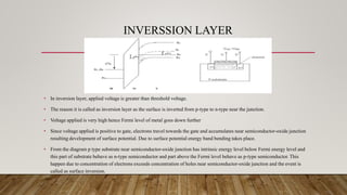
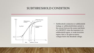
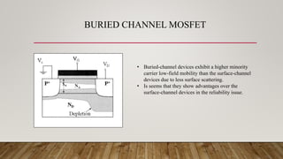
WELCOME
PRESENTED BY:
SABA RATHINAM V
PONDICHERRY UNIVERSITY
M.TECH (1st YEAR)
METAL OXIDE
SEMICONDUCTOR
FIELD EFFECT
TRANSISTOR
MOSFET
CONTENTS
• Introduction
• Structure
• Working Principle
• Band Diagram
• I-V AND C-V Characteristics
• MOSFET Breakdown
• Subthreshold condition
• Buried Channel MOSFET
• Advantages and Disadvantages
• Applications
INTRODUCTION
• MOSFET also known as the metal–oxide–
silicon transistor (MOS transistor,
or MOS), is a type of insulated-gate field-
effect transistor that is fabricated by
the controlled oxidation of a semiconductor,
typically silicon.
• The voltage of the covered gate determines
the electrical conductivity of the device; this
ability to change conductivity with the
amount of applied voltage can be used
for amplifying or switching electronic
signals.
STRUCTURE
WORKING PRINCIPLE
• The working principle of MOSEFT depends up on the MOS capacitor.
• The MOS capacitor is the main part.
• The semiconductor surface a below the oxide layer and between the drain and source
terminal can bd inverted from p-type to n-type by applying a positive or negative gate
voltage respectively.
• When we apply positive gate voltage the holes present beneath the oxide layer
experiencing repulsive force and the holes are pushed downward with the substrate.
BAND DIAGRAM
• MOS capacitor is an equilibrium device i.e. when the external voltage is not applied to the
device the Fermi level of metal and semiconductor are at same level.
• When external voltage is applied to device it behaves according to the voltage applied
with respect to flat band voltage and threshold voltage.
• Flat band voltage is defined as a work function difference between the gate metal and the
semiconductor when no charge is present in oxide-semiconductor interface.
• Threshold voltage is defined as the minimum gate-to-source voltage required to induce or
create a conducting channel. This can be divided into three types.
ACCUMULATOR LAYER
• In this case, applied voltage (Vg)(Vg) is less than flat band voltage. Voltage applied to gate(on metal side) is
negative.
• When voltage is applied, mosfet no longer remain in equilibrium condition. The Fermi energy level of metal
changes by charge of electron multiplied by applied voltage. Voltage applied is negative and hence rise in Fermi
level of metal takes place while Fermi level of semiconductor remain constant.
Where
Ec= conduction band energy
level
Ef= Fermi energy level
Ev= valance band energy level
Ei = intrinsic energy level
Q = charge of electron
Vg=voltage applied on gate
Φs=surface voltage
DEPLETION LAYER
• In depletion region, voltage applied to gate is greater than flat band voltage and less than threshold voltage.
• n this case, voltage applied to gate is positive hence there is fall in Fermi energy level of metal while rise in
Fermi energy level of semiconductor.
• Since voltage applied to positive and hence positive charge develops near metal-oxide junction thus the
electrons travel towards the gate creating negative charge near oxide-semiconductor junction.
• Electrons recombine with holes present near oxide creating depletion region.
• Surface voltage develops in depletion region and effect of this we have energy band bending in depletion region.
INVERSSION LAYER
• In inversion layer, applied voltage is greater than threshold voltage.
• The reason it is called as inversion layer as the surface is inverted from p-type to n-type near the junction.
• Voltage applied is very high hence Fermi level of metal goes down further
• Since voltage applied is positive to gate, electrons travel towards the gate and accumulates near semiconductor-oxide junction
resulting development of surface potential. Due to surface potential energy band bending takes place.
• From the diagram p type substrate near semiconductor-oxide junction has intrinsic energy level below Fermi energy level and
this part of substrate behave as n-type semiconductor and part above the Fermi level behave as p-type semiconductor. This
happen due to concentration of electrons exceeds concentration of holes near semiconductor-oxide junction and the event is
called as surface inversion.
C-V CHARACTERISTICS
• Consider the terminal connections of n-channel
MOSFET shown in Figure below.
• Which consists of Vs = 0, Vd = 0 and Vb = 0
and a bias is applied to the gate terminal.
• Depending upon the gate bias there are different
regions of operation in C-V curve that are
accumulation, depletion and strong inversion.
• We will discuss each region of operation in details
in this section.
I-V CHARACTERISTICS
• It is a graph of drain current Id versus drain to
source voltage VDS for different values of the
gate to source voltage VGS. It has three regions;
saturation, cut-off, and ohmic region. In the
application where the MOSFET used as a
switch, the device works in the cut-off region
and ohmic region when turned OFF and ON
respectively. The operation in the saturation
region avoided reducing the power dissipation in
the on-state.
• When the gate-source voltage is less than the
threshold voltage, the MOSFET is in the cut-off
state. To avoid breakdown the drain to source
breakdown voltage should be greater than the
applied voltage. The avalanche breakdown takes
place.
• The power MOSFET goes into the ohmic region when a larger positive gate to source voltage apply and the drain to source
voltage is small. In this region, the power dissipation is low.
• In the saturation region, the drain current is almost independent of the drain to source voltage. It is only dependent on the gate
to source voltage. The gate voltage is greater than the threshold voltage. The drain current increase with the increase in the gate
to source voltage.
MOSFET BRESKDOWN
• MOSFETs typically operate in three regimes
depending on the drain-source voltage for a given
gate voltage.
• Initially the current-voltage relation is linear, this
is the Linear region.
• As the drain-source voltage increases the
extracted current begins to saturate, this is the
saturation region.
• As the drain-source voltage is further increased
the breakdown region is entered, where the
current increases exponentially for a small
increase in the applied voltage.
• This is due to impact ionization.
SUBTHRESHOLD CONDITION
• Subthreshold conduction or subthreshold
leakage or subthreshold drain current is
the current between the source and drain
of a MOSFET when the transistor is in
subthreshold region, or weak-inversion
region, that is, for gate-to-source
voltages below the threshold voltage.
BURIED CHANNEL MOSFET
• Buried-channel devices exhibit a higher minority
carrier low-field mobility than the surface-channel
devices due to less surface scattering.
• Is seems that they show advantages over the
surface-channel devices in the reliability issue.
ADVANTAGES OF MOSFET
• They can be operated in either enhancement mode or depletion mode.
• They have much higher input impedance compare to JFET.
• They have high drain resistance due to lower resistance of channel.
• They are easy to manufacture.
• They support high speed of operation compare to JFETs.
DISADVANTAGRES OF MOSFET
• The layer between gate and channel is very fragile which is vulnerable to electro-static
damage during installation.
• It requires well designed circuit to avoid the issue.
• MOSFET is very susceptible to overload voltages, hence special handling is required
during installation.
APPLICATIONS OF MOSFET
• MOSFET is used for switching and amplifying electronics signals in the electronic
devices.
• It is used as an inverter.
• It can be used in digital circuit.
• It can be used as a high frequency amplifier.
• MOSFET can be used as a passive element. (Resistor, Capacitor, Inductor).
• It can be used in brushless DC motor drive.
• It can be used in electronic DC relay.
• It can be used in switch mode power supply (SMPS).
THANK YOU

MOSFET

  • 1.
    WELCOME PRESENTED BY: SABA RATHINAMV PONDICHERRY UNIVERSITY M.TECH (1st YEAR)
  • 2.
  • 3.
    CONTENTS • Introduction • Structure •Working Principle • Band Diagram • I-V AND C-V Characteristics • MOSFET Breakdown • Subthreshold condition • Buried Channel MOSFET • Advantages and Disadvantages • Applications
  • 4.
    INTRODUCTION • MOSFET alsoknown as the metal–oxide– silicon transistor (MOS transistor, or MOS), is a type of insulated-gate field- effect transistor that is fabricated by the controlled oxidation of a semiconductor, typically silicon. • The voltage of the covered gate determines the electrical conductivity of the device; this ability to change conductivity with the amount of applied voltage can be used for amplifying or switching electronic signals.
  • 5.
  • 6.
    WORKING PRINCIPLE • Theworking principle of MOSEFT depends up on the MOS capacitor. • The MOS capacitor is the main part. • The semiconductor surface a below the oxide layer and between the drain and source terminal can bd inverted from p-type to n-type by applying a positive or negative gate voltage respectively. • When we apply positive gate voltage the holes present beneath the oxide layer experiencing repulsive force and the holes are pushed downward with the substrate.
  • 7.
    BAND DIAGRAM • MOScapacitor is an equilibrium device i.e. when the external voltage is not applied to the device the Fermi level of metal and semiconductor are at same level. • When external voltage is applied to device it behaves according to the voltage applied with respect to flat band voltage and threshold voltage. • Flat band voltage is defined as a work function difference between the gate metal and the semiconductor when no charge is present in oxide-semiconductor interface. • Threshold voltage is defined as the minimum gate-to-source voltage required to induce or create a conducting channel. This can be divided into three types.
  • 8.
    ACCUMULATOR LAYER • Inthis case, applied voltage (Vg)(Vg) is less than flat band voltage. Voltage applied to gate(on metal side) is negative. • When voltage is applied, mosfet no longer remain in equilibrium condition. The Fermi energy level of metal changes by charge of electron multiplied by applied voltage. Voltage applied is negative and hence rise in Fermi level of metal takes place while Fermi level of semiconductor remain constant. Where Ec= conduction band energy level Ef= Fermi energy level Ev= valance band energy level Ei = intrinsic energy level Q = charge of electron Vg=voltage applied on gate Φs=surface voltage
  • 9.
    DEPLETION LAYER • Indepletion region, voltage applied to gate is greater than flat band voltage and less than threshold voltage. • n this case, voltage applied to gate is positive hence there is fall in Fermi energy level of metal while rise in Fermi energy level of semiconductor. • Since voltage applied to positive and hence positive charge develops near metal-oxide junction thus the electrons travel towards the gate creating negative charge near oxide-semiconductor junction. • Electrons recombine with holes present near oxide creating depletion region. • Surface voltage develops in depletion region and effect of this we have energy band bending in depletion region.
  • 10.
    INVERSSION LAYER • Ininversion layer, applied voltage is greater than threshold voltage. • The reason it is called as inversion layer as the surface is inverted from p-type to n-type near the junction. • Voltage applied is very high hence Fermi level of metal goes down further • Since voltage applied is positive to gate, electrons travel towards the gate and accumulates near semiconductor-oxide junction resulting development of surface potential. Due to surface potential energy band bending takes place. • From the diagram p type substrate near semiconductor-oxide junction has intrinsic energy level below Fermi energy level and this part of substrate behave as n-type semiconductor and part above the Fermi level behave as p-type semiconductor. This happen due to concentration of electrons exceeds concentration of holes near semiconductor-oxide junction and the event is called as surface inversion.
  • 11.
    C-V CHARACTERISTICS • Considerthe terminal connections of n-channel MOSFET shown in Figure below. • Which consists of Vs = 0, Vd = 0 and Vb = 0 and a bias is applied to the gate terminal. • Depending upon the gate bias there are different regions of operation in C-V curve that are accumulation, depletion and strong inversion. • We will discuss each region of operation in details in this section.
  • 12.
    I-V CHARACTERISTICS • Itis a graph of drain current Id versus drain to source voltage VDS for different values of the gate to source voltage VGS. It has three regions; saturation, cut-off, and ohmic region. In the application where the MOSFET used as a switch, the device works in the cut-off region and ohmic region when turned OFF and ON respectively. The operation in the saturation region avoided reducing the power dissipation in the on-state. • When the gate-source voltage is less than the threshold voltage, the MOSFET is in the cut-off state. To avoid breakdown the drain to source breakdown voltage should be greater than the applied voltage. The avalanche breakdown takes place. • The power MOSFET goes into the ohmic region when a larger positive gate to source voltage apply and the drain to source voltage is small. In this region, the power dissipation is low. • In the saturation region, the drain current is almost independent of the drain to source voltage. It is only dependent on the gate to source voltage. The gate voltage is greater than the threshold voltage. The drain current increase with the increase in the gate to source voltage.
  • 13.
    MOSFET BRESKDOWN • MOSFETstypically operate in three regimes depending on the drain-source voltage for a given gate voltage. • Initially the current-voltage relation is linear, this is the Linear region. • As the drain-source voltage increases the extracted current begins to saturate, this is the saturation region. • As the drain-source voltage is further increased the breakdown region is entered, where the current increases exponentially for a small increase in the applied voltage. • This is due to impact ionization.
  • 14.
    SUBTHRESHOLD CONDITION • Subthresholdconduction or subthreshold leakage or subthreshold drain current is the current between the source and drain of a MOSFET when the transistor is in subthreshold region, or weak-inversion region, that is, for gate-to-source voltages below the threshold voltage.
  • 15.
    BURIED CHANNEL MOSFET •Buried-channel devices exhibit a higher minority carrier low-field mobility than the surface-channel devices due to less surface scattering. • Is seems that they show advantages over the surface-channel devices in the reliability issue.
  • 16.
    ADVANTAGES OF MOSFET •They can be operated in either enhancement mode or depletion mode. • They have much higher input impedance compare to JFET. • They have high drain resistance due to lower resistance of channel. • They are easy to manufacture. • They support high speed of operation compare to JFETs.
  • 17.
    DISADVANTAGRES OF MOSFET •The layer between gate and channel is very fragile which is vulnerable to electro-static damage during installation. • It requires well designed circuit to avoid the issue. • MOSFET is very susceptible to overload voltages, hence special handling is required during installation.
  • 18.
    APPLICATIONS OF MOSFET •MOSFET is used for switching and amplifying electronics signals in the electronic devices. • It is used as an inverter. • It can be used in digital circuit. • It can be used as a high frequency amplifier. • MOSFET can be used as a passive element. (Resistor, Capacitor, Inductor). • It can be used in brushless DC motor drive. • It can be used in electronic DC relay. • It can be used in switch mode power supply (SMPS).
  • 19.