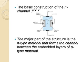
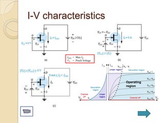
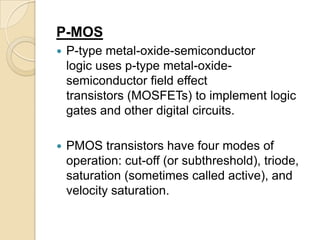
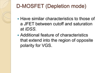
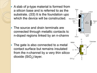
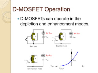
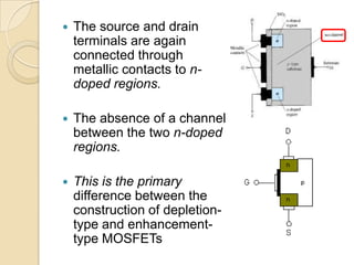
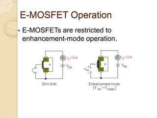
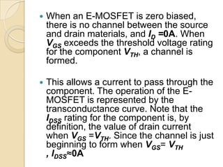
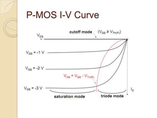
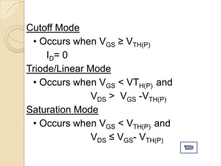
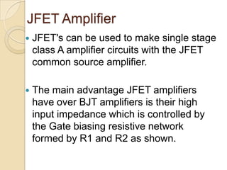
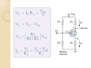
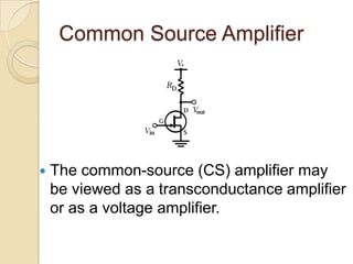
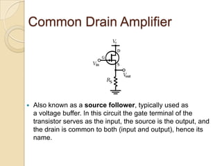
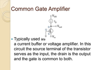
CHAPTER 5
 EE201-SEMICONDUCTOR DEVICES


  FIELD EFFECT
TRANSISTORS (FET)
                     BY
         PN. RUHIYAH NAZIHAH ZAHKAI
    ELECTRICAL ENGINEERING DEPARTMENT
       POLYTECHNIC SULTAN IDRIS SHAH
Introduction
   The field-effect transistor (FET) is a three-
    terminal device used for a variety of applications
    that match, to a large extent, those of the BJT
    Although there are important differences between
    the two types of devices.

   The primary difference between the two types of
    transistors is the fact that the
    ◦ BJT transistor is a current-controlled device
    ◦ JFET transistor is a voltage-controlled device

   In each case the current of the output circuit is
    being controlled by a parameter of the input
    circuit—in one case a current level and in the
    other an applied voltage.
   Two types of FETs will be introduced in
    this chapter :
    ◦ Junction Field-Effect Transistor (JFET)
    ◦ Metal-Oxide-Semiconductor Field-Effect
      Transistor (MOSFET)
JFET
 JFET is a three-terminal device with
  one terminal capable of controlling the
  current between the other two.
 For the JFET transistor the n-channel
  device will appear as the prominent
  device than p-channel.
   The basic construction of the n-
    channel JFET .


   The major part of the structure is the
    n-type material that forms the channel
    between the embedded layers of p-
    type material.
   The top of the n-type channel is
    connected through an ohmic contact
    to a terminal referred to as the drain
    (D).

   The lower end of the same material is
    connected through an ohmic contact
    to a terminal referred to as the source
    (S).

   The two p-type materials are
Physical structure
Schematic Symbol


N-Channel      P-Channel
I-V characteristics


         IDSS = Max ID
         VP = Pinch Voltage


                              Operating
                              region
MOSFET
   The metal–oxide–semiconductor field-effect
    transistor (MOSFET, MOS-FET, or MOS FET) is
    a transistor used for amplifying or switching
    electronic signals.

   In MOSFETs, a voltage on the oxide-insulated
    gate electrode can induce a conducting
    channel between the two other contacts called
    source and drain.

   The channel can be of n-type or p-type, called an
    nMOSFET or a pMOSFET (also commonly
    nMOS, pMOS).

   MOSFET is further broken down into depletion
    and enhancement types.
N-MOS & P-MOS
N-MOS
   n-channel MOSFETs are smaller than p-
    channel MOSFETs and producing only one
    type of MOSFET on a silicon substrate is
    cheaper and technically simpler.
P-MOS
   P-type metal-oxide-semiconductor
    logic uses p-type metal-oxide-
    semiconductor field effect
    transistors (MOSFETs) to implement logic
    gates and other digital circuits.

   PMOS transistors have four modes of
    operation: cut-off (or subthreshold), triode,
    saturation (sometimes called active), and
    velocity saturation.
Physical & Schematic
diagram
D-MOSFET (Depletion mode)

 Have similar characteristics to those of
  a JFET between cutoff and saturation
  at IDSS.
 Additional feature of characteristics
  that extend into the region of opposite
  polarity for VGS.
   A slab of p-type material is formed from
    a silicon base and is referred to as the
    substrate. (SS) It is the foundation upon
    which the device will be constructed.

   The source and drain terminals are
    connected through metallic contacts to
    n-doped regions linked by an n-channel

   The gate is also connected to a metal
    contact surface but remains insulated
    from the n-channel by a very thin silicon
    dioxide (SiO2) layer.
D-MOSFET Operation
    D-MOSFETs can operate in the
     depletion and enhancement modes.
   Zero bias: The gate is shorted to the source, so
    drain current equals the IDSS rating of the
    component.

   Depletion mode: The negative gate-source
    voltage forces free electrons away from the gate,
    forming a depletion layer that cuts into the
    channel. As a result,
     ID < IDSS

   Enhancement mode: The positive gate-source
    voltage attracts free electrons in the substrate
    toward the channel while driving valence-band
    holes (in the substrate) away from the channel. As
    a result, the material to the right of the channel
    effectively becomes n-type material. ID > IDSS.
E-MOSFET
   There are some similarities in construction and
    mode of operation between depletion-type and
    enhancement-type MOSFETs

   The characteristics of the enhancement-type
    MOSFET are quite different from anything
    obtained thus far.

   Current control in an n-channel device is now
    effected by a positive gate-to-source voltage
    rather than the range of negative voltages
    encountered in n-channel depletion-type
    MOSFETs.
   The source and drain
    terminals are again
    connected through
    metallic contacts to n-
    doped regions.

   The absence of a channel
    between the two n-doped
    regions.

   This is the primary
    difference between the
    construction of depletion-
    type and enhancement-
    type MOSFETs
E-MOSFET Operation
   E-MOSFETs are restricted to
    enhancement-mode operation.
   When an E-MOSFET is zero biased,
    there is no channel between the source
    and drain materials, and ID =0A. When
    VGS exceeds the threshold voltage rating
    for the component VTH, a channel is
    formed.

   This allows a current to pass through the
    component. The operation of the E-
    MOSFET is represented by the
    transconductance curve. Note that the
    IDSS rating for the component is, by
    definition, the value of drain current
    when VGS =VTH. Since the channel is just
    beginning to form when VGS= VTH
    , IDSS≈0A
NMOS I-V Characteristics
Cutoff Mode
 • Occurs when VGS ≤ VTH(N)
    ID= 0

Triode/Linear Mode
  • Occurs when VGS > VTH(N) and
               VDS < VGS-VTH(N)

Saturation Mode
 • Occurs when VGS > VTH(N) and
              VDS ≥ VGS -VTH(N)
PMOS IV Characteristics
•    ID, VGS, VDS, and VTH(P) are all negative
    for PMOS.

•   Channel formed when VGS < VTH(P)

•   Saturation occurs when VDS ≤ VGS –
    VTH(P)
P-MOS I-V Curve
Cutoff Mode
 • Occurs when VGS ≥ VTH(P)
     ID= 0
Triode/Linear Mode
 • Occurs when VGS < VTH(P) and
               VDS > VGS -VTH(P)
Saturation Mode
 • Occurs when VGS < VTH(P) and
               VDS ≤ VGS- VTH(P)
JFET Amplifier
   JFET's can be used to make single stage
    class A amplifier circuits with the JFET
    common source amplifier.

   The main advantage JFET amplifiers
    have over BJT amplifiers is their high
    input impedance which is controlled by
    the Gate biasing resistive network
    formed by R1 and R2 as shown.
   The control of the Drain current by a
    negative Gate potential makes
    the Junction Field Effect Transistor
    useful as a switch.

   It is essential that the Gate voltage is
    never positive for an N-channel JFET as
    the channel current will flow to the Gate
    and not the Drain resulting in damage to
    the JFET.

   The principals of operation for a P-channel
    JFET are the same as for the N-channel
    JFET, except that the polarity of the
    voltages need to be reversed.
   The FET can be used as a linear amplifier
    or as a digital device in logic circuits.

   The enhancement MOSFET is quite
    popular in digital circuitry, especially in
    CMOS circuits that require very low power
    consumption.

   FET devices are also widely used in high-
    frequency applications and in buffering
    (interfacing) applications.
Common Source Amplifier


   The common-source (CS) amplifier may
    be viewed as a transconductance amplifier
    or as a voltage amplifier.
   As a transconductance amplifier, the input
    voltage is seen as modulating the current
    going to the load.

   As a voltage amplifier, input voltage
    modulates the amount of current flowing
    through the FET, changing the voltage
    across the output resistance according
    to Ohm's law.

   FET device's output resistance typically is
    not high enough for a reasonable
    transconductance amplifier (ideally infinite),
    nor low enough for a decent voltage
    amplifier (ideally zero).
Common Drain Amplifier


   Also known as a source follower, typically used as
    a voltage buffer. In this circuit the gate terminal of the
    transistor serves as the input, the source is the output, and
    the drain is common to both (input and output), hence its
    name.
   In addition, this circuit is used to
    transform impedances.
    ◦ For example, the Thévenin resistance of a
      combination of a voltage follower driven by a
      voltage source with high Thévenin resistance is
      reduced to only the output resistance of the
      voltage follower, a small resistance. That
      resistance reduction makes the combination a
      more ideal voltage source.

   Conversely, a voltage follower inserted
    between a driving stage and a high load (ie a
    low resistance) presents an infinite resistance
    (low load) to the driving stage, an advantage
    in coupling a voltage signal to a large load.
Common Gate Amplifier


   Typically used as
    a current buffer or voltage amplifier. In this
    circuit the source terminal of the transistor
    serves as the input, the drain is the output
    and the gate is common to both.
   This configuration is used less often
    than the common source or source
    follower.

   Usually used in CMOS RF receivers
    for ease of impedance matching and
    potentially has lower noise.
MOSFET as Switches
   MOSFET switches use the MOSFET
    channel as a low–on-resistance switch
    to pass analog signals when on, and
    as a high impedance when off.

   In this application the drain and source
    of a MOSFET exchange places
    depending on the voltages of each
    electrode compared to that of the
    gate.
   For a simple MOSFET without an
    integrated diode, the source is the
    more negative side for an N-MOS or
    the more positive side for a P-MOS.
    All of these switches are limited on
    what signals they can pass or stop by
    their gate-source, gate-drain and
    source-drain voltages, and source-to-
    drain currents; exceeding the voltage
    limits will potentially damage the
    switch.
MOSFET CHARACTERISTIC
CURVE
1. Cut-off Region
 Here the operating conditions of the
  transistor are zero input gate voltage
  ( VIN ), zero drain current IDand output
  voltage VDS = VDD Therefore the MOSFET
  is switched "Fully-OFF".
Saturation Region
 Here the transistor will be biased so that
  the maximum amount of gate voltage is
  applied to the device which results in the
  channel resistance RDS(on) being as small
  as possible with maximum drain current
  flowing through the MOSFET switch.
  Therefore the MOSFET is switched "Fully-
  ON".
N-MOS as switch


•The input and Gate are grounded (0v)
•Gate-source voltage less than threshold voltage VGS < VTH
•MOSFET is "fully-OFF" (Cut-off region)
•No Drain current flows ( ID = 0 )
•VOUT = VDS = VDD = "1"
•MOSFET operates as an "open switch"

Then we can define the "cut-off region" or "OFF mode" of a MOSFET
switch as being, gate voltage,VGS < VTH and ID = 0. For a P-channel
MOSFET, the gate potential must be negative.
•The input and Gate are connected to VDD
•Gate-source voltage is much greater than threshold voltage VGS > VTH
•MOSFET is "fully-ON" (saturation region)
•Max Drain current flows ( ID = VDD / RL )
•VDS = 0V (ideal saturation)
•Min channel resistance RDS(on) < 0.1Ω
•VOUT = VDS = 0.2V (RDS.ID)
•MOSFET operates as a "closed switch"

Then we can define the "saturation region" or "ON mode" of a MOSFET
switch as gate-source voltage,VGS > VTH and ID = Maximum. For a P-channel
MOSFET, the gate potential must be positive.
P-channel MOSFET Switch
APPLICATION MOSFET AS
SWITCH
   In this circuit arrangement an Enhancement-
    mode N-channel MOSFET is being used to
    switch a simple lamp "ON" and "OFF" (could
    also be an LED). The gate input
    voltage VGS is taken to an appropriate
    positive voltage level to turn the device and
    therefore the lamp either fully "ON",
    ( VGS = +ve ) or at a zero voltage level that
    turns the device fully "OFF", ( VGS = 0).
   If the resistive load of the lamp was to be
    replaced by an inductive load such as a coil,
    solenoid or relay a "flywheel diode" would be
    required in parallel with the load to protect
    the MOSFET from any self generated back-
    emf.
   In a P-channel device the conventional flow of
    drain current is in the negative direction so a
    negative gate-source voltage is applied to switch
    the transistor "ON". This is achieved because the
    P-channel MOSFET is "upside down" with its
    source terminal tied to the positive supply +VDD.
    Then when the switch goes LOW, the MOSFET
    turns "ON" and when the switch goes HIGH the
    MOSFET turns "OFF".

   This upside down connection of a P-channel
    enhancement mode MOSFET switch allows us to
    connect it in series with a N-channel enhancement
    mode MOSFET to produce a complementary or
    CMOS switching device as shown across a dual
    supply.

EE20-Chapter 5

  • 1.
    CHAPTER 5 EE201-SEMICONDUCTORDEVICES FIELD EFFECT TRANSISTORS (FET) BY PN. RUHIYAH NAZIHAH ZAHKAI ELECTRICAL ENGINEERING DEPARTMENT POLYTECHNIC SULTAN IDRIS SHAH
  • 2.
    Introduction  The field-effect transistor (FET) is a three- terminal device used for a variety of applications that match, to a large extent, those of the BJT Although there are important differences between the two types of devices.  The primary difference between the two types of transistors is the fact that the ◦ BJT transistor is a current-controlled device ◦ JFET transistor is a voltage-controlled device  In each case the current of the output circuit is being controlled by a parameter of the input circuit—in one case a current level and in the other an applied voltage.
  • 3.
    Two types of FETs will be introduced in this chapter : ◦ Junction Field-Effect Transistor (JFET) ◦ Metal-Oxide-Semiconductor Field-Effect Transistor (MOSFET)
  • 4.
    JFET  JFET isa three-terminal device with one terminal capable of controlling the current between the other two.  For the JFET transistor the n-channel device will appear as the prominent device than p-channel.
  • 5.
    The basic construction of the n- channel JFET .  The major part of the structure is the n-type material that forms the channel between the embedded layers of p- type material.
  • 6.
    The top of the n-type channel is connected through an ohmic contact to a terminal referred to as the drain (D).  The lower end of the same material is connected through an ohmic contact to a terminal referred to as the source (S).  The two p-type materials are
  • 7.
  • 8.
  • 9.
    I-V characteristics IDSS = Max ID VP = Pinch Voltage Operating region
  • 10.
    MOSFET  The metal–oxide–semiconductor field-effect transistor (MOSFET, MOS-FET, or MOS FET) is a transistor used for amplifying or switching electronic signals.  In MOSFETs, a voltage on the oxide-insulated gate electrode can induce a conducting channel between the two other contacts called source and drain.  The channel can be of n-type or p-type, called an nMOSFET or a pMOSFET (also commonly nMOS, pMOS).  MOSFET is further broken down into depletion and enhancement types.
  • 11.
    N-MOS & P-MOS N-MOS  n-channel MOSFETs are smaller than p- channel MOSFETs and producing only one type of MOSFET on a silicon substrate is cheaper and technically simpler.
  • 12.
    P-MOS  P-type metal-oxide-semiconductor logic uses p-type metal-oxide- semiconductor field effect transistors (MOSFETs) to implement logic gates and other digital circuits.  PMOS transistors have four modes of operation: cut-off (or subthreshold), triode, saturation (sometimes called active), and velocity saturation.
  • 13.
  • 14.
    D-MOSFET (Depletion mode) Have similar characteristics to those of a JFET between cutoff and saturation at IDSS.  Additional feature of characteristics that extend into the region of opposite polarity for VGS.
  • 15.
    A slab of p-type material is formed from a silicon base and is referred to as the substrate. (SS) It is the foundation upon which the device will be constructed.  The source and drain terminals are connected through metallic contacts to n-doped regions linked by an n-channel  The gate is also connected to a metal contact surface but remains insulated from the n-channel by a very thin silicon dioxide (SiO2) layer.
  • 16.
    D-MOSFET Operation  D-MOSFETs can operate in the depletion and enhancement modes.
  • 17.
    Zero bias: The gate is shorted to the source, so drain current equals the IDSS rating of the component.  Depletion mode: The negative gate-source voltage forces free electrons away from the gate, forming a depletion layer that cuts into the channel. As a result, ID < IDSS  Enhancement mode: The positive gate-source voltage attracts free electrons in the substrate toward the channel while driving valence-band holes (in the substrate) away from the channel. As a result, the material to the right of the channel effectively becomes n-type material. ID > IDSS.
  • 18.
    E-MOSFET  There are some similarities in construction and mode of operation between depletion-type and enhancement-type MOSFETs  The characteristics of the enhancement-type MOSFET are quite different from anything obtained thus far.  Current control in an n-channel device is now effected by a positive gate-to-source voltage rather than the range of negative voltages encountered in n-channel depletion-type MOSFETs.
  • 19.
    The source and drain terminals are again connected through metallic contacts to n- doped regions.  The absence of a channel between the two n-doped regions.  This is the primary difference between the construction of depletion- type and enhancement- type MOSFETs
  • 20.
    E-MOSFET Operation  E-MOSFETs are restricted to enhancement-mode operation.
  • 21.
    When an E-MOSFET is zero biased, there is no channel between the source and drain materials, and ID =0A. When VGS exceeds the threshold voltage rating for the component VTH, a channel is formed.  This allows a current to pass through the component. The operation of the E- MOSFET is represented by the transconductance curve. Note that the IDSS rating for the component is, by definition, the value of drain current when VGS =VTH. Since the channel is just beginning to form when VGS= VTH , IDSS≈0A
  • 22.
  • 23.
    Cutoff Mode •Occurs when VGS ≤ VTH(N) ID= 0 Triode/Linear Mode • Occurs when VGS > VTH(N) and VDS < VGS-VTH(N) Saturation Mode • Occurs when VGS > VTH(N) and VDS ≥ VGS -VTH(N)
  • 24.
    PMOS IV Characteristics • ID, VGS, VDS, and VTH(P) are all negative for PMOS. • Channel formed when VGS < VTH(P) • Saturation occurs when VDS ≤ VGS – VTH(P)
  • 25.
  • 26.
    Cutoff Mode •Occurs when VGS ≥ VTH(P) ID= 0 Triode/Linear Mode • Occurs when VGS < VTH(P) and VDS > VGS -VTH(P) Saturation Mode • Occurs when VGS < VTH(P) and VDS ≤ VGS- VTH(P)
  • 27.
    JFET Amplifier  JFET's can be used to make single stage class A amplifier circuits with the JFET common source amplifier.  The main advantage JFET amplifiers have over BJT amplifiers is their high input impedance which is controlled by the Gate biasing resistive network formed by R1 and R2 as shown.
  • 29.
    The control of the Drain current by a negative Gate potential makes the Junction Field Effect Transistor useful as a switch.  It is essential that the Gate voltage is never positive for an N-channel JFET as the channel current will flow to the Gate and not the Drain resulting in damage to the JFET.  The principals of operation for a P-channel JFET are the same as for the N-channel JFET, except that the polarity of the voltages need to be reversed.
  • 30.
    The FET can be used as a linear amplifier or as a digital device in logic circuits.  The enhancement MOSFET is quite popular in digital circuitry, especially in CMOS circuits that require very low power consumption.  FET devices are also widely used in high- frequency applications and in buffering (interfacing) applications.
  • 31.
    Common Source Amplifier  The common-source (CS) amplifier may be viewed as a transconductance amplifier or as a voltage amplifier.
  • 32.
    As a transconductance amplifier, the input voltage is seen as modulating the current going to the load.  As a voltage amplifier, input voltage modulates the amount of current flowing through the FET, changing the voltage across the output resistance according to Ohm's law.  FET device's output resistance typically is not high enough for a reasonable transconductance amplifier (ideally infinite), nor low enough for a decent voltage amplifier (ideally zero).
  • 33.
    Common Drain Amplifier  Also known as a source follower, typically used as a voltage buffer. In this circuit the gate terminal of the transistor serves as the input, the source is the output, and the drain is common to both (input and output), hence its name.
  • 34.
    In addition, this circuit is used to transform impedances. ◦ For example, the Thévenin resistance of a combination of a voltage follower driven by a voltage source with high Thévenin resistance is reduced to only the output resistance of the voltage follower, a small resistance. That resistance reduction makes the combination a more ideal voltage source.  Conversely, a voltage follower inserted between a driving stage and a high load (ie a low resistance) presents an infinite resistance (low load) to the driving stage, an advantage in coupling a voltage signal to a large load.
  • 35.
    Common Gate Amplifier  Typically used as a current buffer or voltage amplifier. In this circuit the source terminal of the transistor serves as the input, the drain is the output and the gate is common to both.
  • 36.
    This configuration is used less often than the common source or source follower.  Usually used in CMOS RF receivers for ease of impedance matching and potentially has lower noise.
  • 37.
    MOSFET as Switches  MOSFET switches use the MOSFET channel as a low–on-resistance switch to pass analog signals when on, and as a high impedance when off.  In this application the drain and source of a MOSFET exchange places depending on the voltages of each electrode compared to that of the gate.
  • 38.
    For a simple MOSFET without an integrated diode, the source is the more negative side for an N-MOS or the more positive side for a P-MOS. All of these switches are limited on what signals they can pass or stop by their gate-source, gate-drain and source-drain voltages, and source-to- drain currents; exceeding the voltage limits will potentially damage the switch.
  • 39.
  • 40.
    1. Cut-off Region Here the operating conditions of the transistor are zero input gate voltage ( VIN ), zero drain current IDand output voltage VDS = VDD Therefore the MOSFET is switched "Fully-OFF".
  • 41.
    Saturation Region  Herethe transistor will be biased so that the maximum amount of gate voltage is applied to the device which results in the channel resistance RDS(on) being as small as possible with maximum drain current flowing through the MOSFET switch. Therefore the MOSFET is switched "Fully- ON".
  • 42.
    N-MOS as switch •Theinput and Gate are grounded (0v) •Gate-source voltage less than threshold voltage VGS < VTH •MOSFET is "fully-OFF" (Cut-off region) •No Drain current flows ( ID = 0 ) •VOUT = VDS = VDD = "1" •MOSFET operates as an "open switch" Then we can define the "cut-off region" or "OFF mode" of a MOSFET switch as being, gate voltage,VGS < VTH and ID = 0. For a P-channel MOSFET, the gate potential must be negative.
  • 43.
    •The input andGate are connected to VDD •Gate-source voltage is much greater than threshold voltage VGS > VTH •MOSFET is "fully-ON" (saturation region) •Max Drain current flows ( ID = VDD / RL ) •VDS = 0V (ideal saturation) •Min channel resistance RDS(on) < 0.1Ω •VOUT = VDS = 0.2V (RDS.ID) •MOSFET operates as a "closed switch" Then we can define the "saturation region" or "ON mode" of a MOSFET switch as gate-source voltage,VGS > VTH and ID = Maximum. For a P-channel MOSFET, the gate potential must be positive.
  • 44.
  • 45.
  • 46.
    In this circuit arrangement an Enhancement- mode N-channel MOSFET is being used to switch a simple lamp "ON" and "OFF" (could also be an LED). The gate input voltage VGS is taken to an appropriate positive voltage level to turn the device and therefore the lamp either fully "ON", ( VGS = +ve ) or at a zero voltage level that turns the device fully "OFF", ( VGS = 0).  If the resistive load of the lamp was to be replaced by an inductive load such as a coil, solenoid or relay a "flywheel diode" would be required in parallel with the load to protect the MOSFET from any self generated back- emf.
  • 47.
    In a P-channel device the conventional flow of drain current is in the negative direction so a negative gate-source voltage is applied to switch the transistor "ON". This is achieved because the P-channel MOSFET is "upside down" with its source terminal tied to the positive supply +VDD. Then when the switch goes LOW, the MOSFET turns "ON" and when the switch goes HIGH the MOSFET turns "OFF".  This upside down connection of a P-channel enhancement mode MOSFET switch allows us to connect it in series with a N-channel enhancement mode MOSFET to produce a complementary or CMOS switching device as shown across a dual supply.