Download as PDF, PPTX


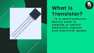
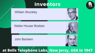
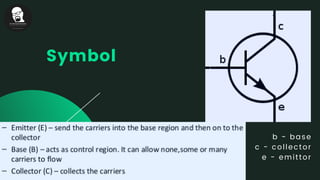
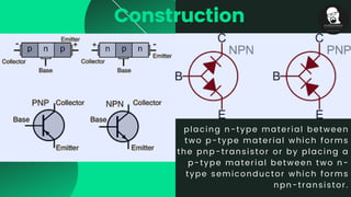


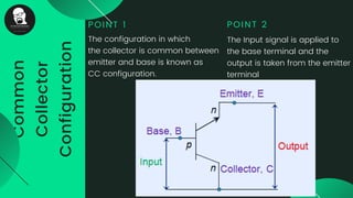
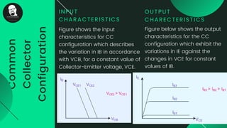
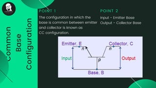
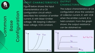
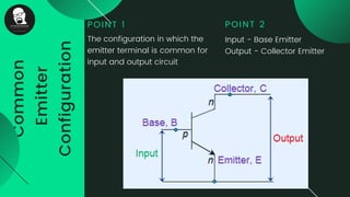
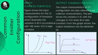
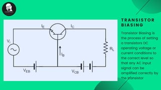

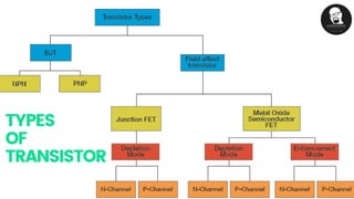


The document provides an overview of transistors, including their definition as semiconductor devices used for amplifying or switching signals and their invention in 1947. It details the structure, configuration types (common collector, common base, common emitter), and explains the biasing process necessary for optimal transistor performance. The document also mentions various applications of transistors in electronic circuits such as amplifiers and switching devices.