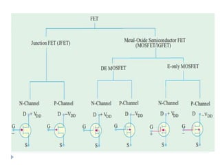
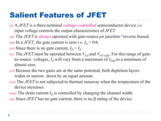
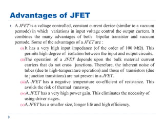
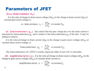
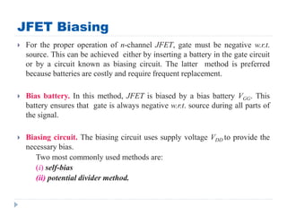
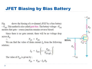
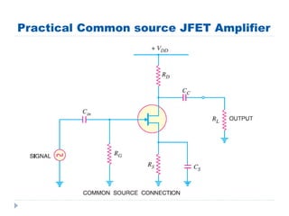
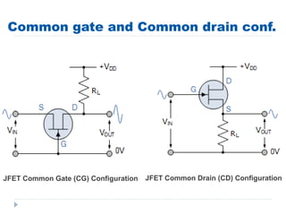
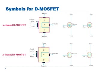
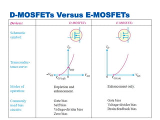
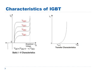
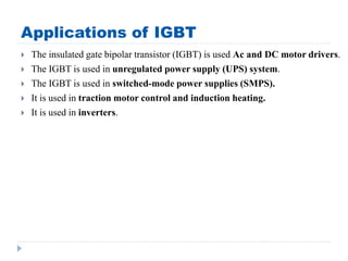
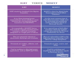
This document provides an overview of field effect transistors (FETs), including their advantages over bipolar junction transistors (BJTs), construction, operation, characteristics, and types. The key types discussed are junction FETs (JFETs), metal-oxide-semiconductor FETs (MOSFETs), which come in depletion and enhancement varieties, and insulated-gate bipolar transistors (IGBTs). JFETs and MOSFETs are described as voltage-controlled devices with high input impedance. IGBTs combine aspects of MOSFETs and BJTs. Common configurations like common source are also covered.
![Expression for Drain Current (ID)
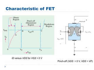
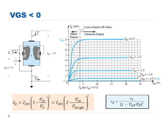
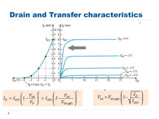
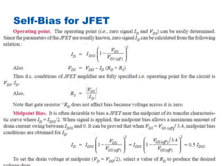
The relation between IDSS and VP is shown in Fig.
We note that gate-source cut off voltage [i.e.VGS (off)] on the transfer characteristic is
equal to pinch off voltage VP on the drain characteristic i.e.
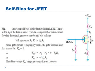
The transfer characteristic of JFET shown in Fig. is part of a parabola. A rather
complex mathematical analysis yields the following expression for drain current :](https://image.slidesharecdn.com/chapter-4fet1-220922182103-28e9aebe/85/Chapter-4-FET-1-ppt-11-320.jpg)
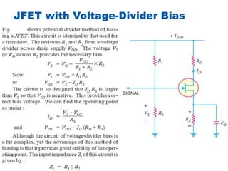
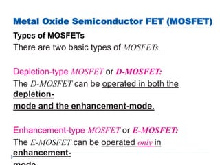
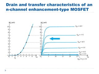
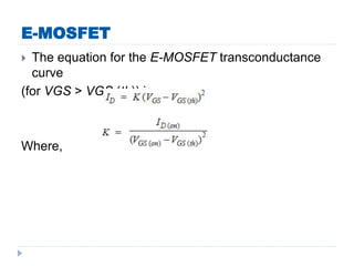
![E-MOSFET
Two things are worth noting about E-MOSFET.
First, E-MOSFET operates only in the enhancement
mode and has no depletion mode.
Secondly, the E-MOSFET has no physical channel
from source to drain.
The minimum value of VGS of proper polarity that
turns on the E-MOSFET is called Threshold voltage
[VGS (th)].](https://image.slidesharecdn.com/chapter-4fet1-220922182103-28e9aebe/85/Chapter-4-FET-1-ppt-28-320.jpg)


![Aim-to study characterstics of fet (field effect [Autosaved].pptx](https://cdn.slidesharecdn.com/ss_thumbnails/aim-tostudycharactersticsoffetfieldeffectautosaved-221113041420-4dcee974-thumbnail.jpg?width=640&height=640&fit=bounds)