Jfet basics
•
5 likes•6,707 views

This document provides an overview of junction field-effect transistors (JFETs), including their basic construction and operation. It develops analytic equations to model JFET behavior, such as equations for drain current, transconductance gain, and normalized parameters. It also compares approximate and more exact mathematical models for JFETs, showing that the approximate model is reasonably accurate while being more convenient.
![JFET Basics
The main feature of JFETs is extremely high input resistance – usually at least several
hundred megohms. This feature enables the power gain of a JFET amplifier to be huge.
Development of analytic equations for JFET bias condition
The following discussion is about n-channel JFETs. p-channel JFETs operate the same
way except that the polarity of the terminal voltages and currents is inverted. There are
two parameters that describe the operation of a JFET:
IDSS is the drain saturation current at VGS = 0.
VP is the gate-source voltage, VGS, that causes the channel conduction to drop to zero
(actually, the drain current does not go all the way to zero but ceases to decrease
below a very small current).
IDSS and VP have a rough proportional relationship. A high IDSS generally has a higher
magnitude VP. However, because the relationship is dependent on the manufacturing
geometry of the JFET there is not a singular proportionality constant. The interpretation
of this is that for the spread of IDSS and VP provided on the data sheet for a specific part
that low values of one parameter tend to correlate with low values of the other parameter
with the same holding true for higher values. Some data sheets show a typical plot of this
relationship.
The drain current is zero when VGS = VP and is IDSS when VGS = 0. The relationship in
the saturation region follows a square law as shown in Equation 1. For normal operation,
VGS is biased to be somewhere between VP and 0. Equation 1 gives the approximate
drain current, ID, for a given bias point. This approximation is generally good to within
about ten percent and is the accepted equation for all JFET calculations. The more exact
model is discussed later.
2
ID = IDSS * [1 - (VGS/VP)] Eq. 1
Equation 1 is valid only if the JFET is operating such that VGS is between 0 and VP and
that VDS is greater than (VGS - VP) , i.e. the saturation region. Note that the drain current,
ID, will be between 0 and IDSS. Figure 2 illustrates an example transfer function for a
JFET that has an IDSS of 12 mA and a VP of -6 volts. The drain current will be less if the
transistor is operating in the ohmic region. Although the transfer curve continues into the
positive bias region we do not normally operate the JFET there except for very small
signals.
2](data:image/gif;base64,R0lGODlhAQABAIAAAAAAAP///yH5BAEAAAAALAAAAAABAAEAAAIBRAA7)
More Related Content
What's hot
What's hot (20)
Viewers also liked
Viewers also liked (18)
Similar to Jfet basics
Similar to Jfet basics (20)
Recently uploaded
Recently uploaded (20)
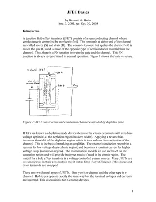
Jfet basics
- 1. JFET Basics by Kenneth A. Kuhn Nov. 3, 2001, rev. Oct. 30, 2008 Introduction A junction field-effect transistor (JFET) consists of a semiconducting channel whose conductance is controlled by an electric field. The terminals at either end of the channel are called source (S) and drain (D). The control electrode that applies the electric field is called the gate (G) and is made of the opposite type of semiconductor material than the channel. Thus, there is a PN junction between the gate and the channel. This PN junction is always reverse biased in normal operation. Figure 1 shows the basic structure. Figure 1: JFET construction and conduction channel controlled by depletion zone JFETs are known as depletion mode devices because the channel conducts with zero bias voltage applied (i.e. the depletion region has zero width). Applying a reverse bias increases the width of the depletion region which in turn reduces the conduction of the channel. This is the basis for making an amplifier. The channel conduction resembles a resistor for low voltage drops (ohmic region) and becomes a constant current for higher voltage drops (saturation region). The mathematical models we use are based on the saturation region and will provide incorrect results if used in the ohmic region. The model for a field effect transistor is a voltage controlled current source. Many JFETs are so symmetrical in their construction that it makes little if any difference if the source and drain terminals are swapped. There are two channel types of JFETs. One type is n-channel and the other type is p- channel. Both types operate exactly the same way but the terminal voltages and currents are inverted. This discussion is for n-channel devices. 1
- 2. JFET Basics The main feature of JFETs is extremely high input resistance – usually at least several hundred megohms. This feature enables the power gain of a JFET amplifier to be huge. Development of analytic equations for JFET bias condition The following discussion is about n-channel JFETs. p-channel JFETs operate the same way except that the polarity of the terminal voltages and currents is inverted. There are two parameters that describe the operation of a JFET: IDSS is the drain saturation current at VGS = 0. VP is the gate-source voltage, VGS, that causes the channel conduction to drop to zero (actually, the drain current does not go all the way to zero but ceases to decrease below a very small current). IDSS and VP have a rough proportional relationship. A high IDSS generally has a higher magnitude VP. However, because the relationship is dependent on the manufacturing geometry of the JFET there is not a singular proportionality constant. The interpretation of this is that for the spread of IDSS and VP provided on the data sheet for a specific part that low values of one parameter tend to correlate with low values of the other parameter with the same holding true for higher values. Some data sheets show a typical plot of this relationship. The drain current is zero when VGS = VP and is IDSS when VGS = 0. The relationship in the saturation region follows a square law as shown in Equation 1. For normal operation, VGS is biased to be somewhere between VP and 0. Equation 1 gives the approximate drain current, ID, for a given bias point. This approximation is generally good to within about ten percent and is the accepted equation for all JFET calculations. The more exact model is discussed later. 2 ID = IDSS * [1 - (VGS/VP)] Eq. 1 Equation 1 is valid only if the JFET is operating such that VGS is between 0 and VP and that VDS is greater than (VGS - VP) , i.e. the saturation region. Note that the drain current, ID, will be between 0 and IDSS. Figure 2 illustrates an example transfer function for a JFET that has an IDSS of 12 mA and a VP of -6 volts. The drain current will be less if the transistor is operating in the ohmic region. Although the transfer curve continues into the positive bias region we do not normally operate the JFET there except for very small signals. 2
- 3. JFET Basics Transfer Curve of a Typical JFET 0.015 0.014 0.013 0.012 0.011 0.010 0.009 0.008 ID 0.007 0.006 0.005 0.004 0.003 0.002 0.001 0.000 -7.0 -6.0 -5.0 -4.0 -3.0 -2.0 -1.0 0.0 VGS Figure 2: Transfer Curve of a Typical JFET showing ID versus VGS Figure 3 shows the family curves for a typical JFET. For amplifiers we normally operate the JFET in the saturation region to the right of the dotted parabola curve that separates the ohmic region from the saturation region. Note that that the dotted curve is the solution to VDS = (VGS – VP). In the ohmic region the device acts similarly to a voltage controlled resistor and in the saturation region the device acts as a voltage controlled current source. The slight tilt of the lines in the saturation region is an extension of the model that includes the effective shunt resistance of the current source. That model is not discussed here. All of the mathematics developed later assumes these lines are perfectly horizontal. It should be noted that for VDS near zero volts (within plus or minus a few tenths of a volt at most) the channel acts as a voltage variable resistor that is linear with voltage. This useful effect continues through zero for small negative voltages across the channel. 3
- 4. FET Family Curves for IDSS = 12 mA and VP = -6 0.015 0.014 Ohmic_region Saturation_region 0.013 VGS=0 0.012 0.011 VGS=-1 0.010 VGS=-2 0.009 0.008 ID VGS=-3 0.007 0.006 VGS=-4 0.005 0.004 VGS=-5 0.003 0.002 VGS=-5.5 0.001 0.000 Knee 0 1 2 3 4 5 6 7 8 9 10 11 12 13 14 15 16 17 18 19 20 VDS Figure 3: FET Family Curves Note: VGS is negative – the minus sign may not show on some systems It is desirable to have the solution to every possible permutation of knowns. The next task is to solve Equation 1 for VGS if ID is known. This is an exercise for the student but the result is: VGS = VP * [1 - sqrt(ID/IDSS)] Eq. 2 Equations 1 and 2 tell us about the DC bias point operation of the JFET for any combination of knowns. Development of gain equations for the JFET Since the JFET is a voltage controlled current source, the gain is the change in drain current divided by the change in gate voltage. This is called the transconductance gain (abbreviated as gm) of the JFET and has units of conductance which is measured in Siemens. The gain value is very low (typically between 0.0001 and 0.02 – but remember that what matters is power gain and that is very high for a JFET) and is often expressed in mS. The gain is found by taking the derivative of Equation 1 with respect to VGS. gm = |2 * (IDSS/VP) * [1 - (VGS/VP)]| Eq. 3
- 5. The absolute value is used because gm is always positive. This is done because sign information is lost when terms are squared as in Equation 1. The ratio, IDSS/VP, will always be negative since VP is negative for n-channel JFETS and IDSS is negative for p- channel JFETS. Note from Equation 3 that gm is a linear function of VGS. When VGS is equal to VP (i.e. ID is zero) then gm is zero. When VGS is equal to zero (i.e. ID = IDSS) then gm is at the maximum value. The maximum value of gm is known as gmo and is obtained by setting VGS to zero in Equation 3. gmo = |2 * (IDSS/VP)| Eq. 4 At this point it should seem obvious that if high gain is desired then the JFET should be biased as close as practical to IDSS. Equation 4 gives us the ultimate gain possible. Equation 3 gives us the gm if VGS is known. For some problems, ID is known instead. Although VGS can be calculated if ID is known, it is convenient to have an equation that directly gives us gm when ID is known. Simple substitution of Equation 1 into Equation 3 (an exercise for the student) gives: gm = |2 * sqrt(ID * IDSS) / VP| Eq. 5 Equation 5 can be expressed in another way that might be convenient for some problems gm = gmo * sqrt(ID/IDSS) Eq. 6 All three ways of computing gm give exactly the same answer. The one to use depends on what the knowns at the moment are. It must be remembered that all of these equations assume the JFET is operating in the saturation region. They do not apply in the ohmic region. The user must always take care in using these equations. The scale factor of 2 in Equations 3 through 5 is nominal. According to the National Semiconductor FET Handbook (1977), that factor can range from about 1.1 to 2.5 but is typically near 2. Keep in mind that we use a model of a JFET based on a simplified quadratic equation. Equations 1 and 2 can be expressed in a normalized form as 2 ID/IDSS = [1 – (VGS/VP)] Eq. 7 VGS/VP = 1 – sqrt(ID/IDSS) Eq. 8
- 6. An equation for the normalized gm can be developed by dividing Equation 3 by Equation 4 producing gm/gmo = 1 – VGS/VP Eq. 9 By substituting Equation 8 into Equation 9 we can also write gm/gmo = sqrt(ID/IDSS) Eq. 10 Figure 4 is a plot of Equations 7 and 9. The linear relationship between VGS and gm is clearly seen. Figure 5 is a plot of Equation 10. Normalized ID/IDSS and gm/gmo versus VGS/VP 1.000 0.900 0.800 0.700 0.600 ID/IDSS ID/IDSS 0.500 gm/gmo 0.400 0.300 0.200 0.100 0.000 0.00 0.10 0.20 0.30 0.40 0.50 0.60 0.70 0.80 0.90 1.00 VGS/VP Figure 4: Normalized FET plot
- 7. gm/gmo versus ID/IDSS 1.000 0.900 0.800 0.700 0.600 gm/gmo 0.500 0.400 0.300 0.200 0.100 0.000 0.000 0.100 0.200 0.300 0.400 0.500 0.600 0.700 0.800 0.900 1.000 ID/IDSS Figure 5: Normalized gm/gmo Comparing “Exact” and Approximate JFET Models In the text, Engineering Electronics, A Practical Approach, by Robert Mauro (copyright 1989 by Prentice-Hall, Inc., Englewood Cliffs, NJ 07632) on pages 209 to 211 there is a development of a more accurate mathematical model for the JFET. The result of that development is: 3/2 [ (VGS) (VGS) ] ID = IDSS * [ 1 – 3 * (-----) + 2 * (-----) ] Eq. 11 [ ( VP ) ( VP ) ] A commonly used and more convenient approximate model was presented in Equation 1 and is expanded here for comparison: 2 [ (VGS) (VGS) ] ID = IDSS * [ 1 – 2 * (-----) + (-----) ] Eq. 12 [ ( VP ) ( VP ) ]
- 8. Figure 6 is a plot of both equations in normalized form. Observe that the error of the approximate model is not very large and that the approximate model predicts a somewhat higher current than the actual. Observe also that the slope of the “exact” curve is steeper thus leading to a higher gm. Comparing "Exact" versus Approximate JFET Models 1.00 0.90 0.80 0.70 0.60 Normalized ID ID approx 0.50 ID exact ID error 0.40 0.30 0.20 0.10 0.00 0.00 0.10 0.20 0.30 0.40 0.50 0.60 0.70 0.80 0.90 1.00 VGS/VP Figure 6: Comparing “Exact” versus Approximate JFET Models Figure 7 shows the normalized transconductance for both models. Observe that the “exact” model has a higher gmo than the approximate model. This is one reason that on data sheets the stated value of gmo is often higher than what one would calculate using the given IDSS and VP parameters.
- 9. Comparing "Exact" gm versus Approximate gm JFET Models 1.40 1.30 1.20 1.10 1.00 0.90 Normalized gm 0.80 gm approx 0.70 gm exact 0.60 0.50 0.40 0.30 0.20 0.10 0.00 0.00 0.10 0.20 0.30 0.40 0.50 0.60 0.70 0.80 0.90 1.00 VGS/VP Figure 7: Comparing “Exact” gm versus Approximate gm JFET Models