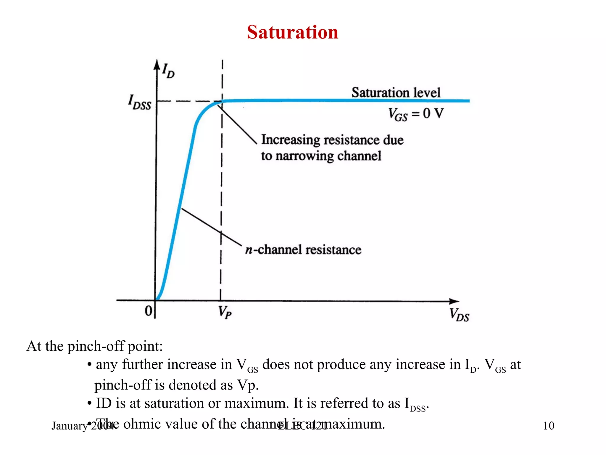
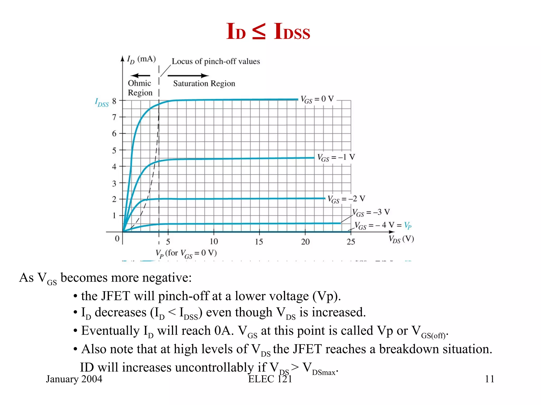
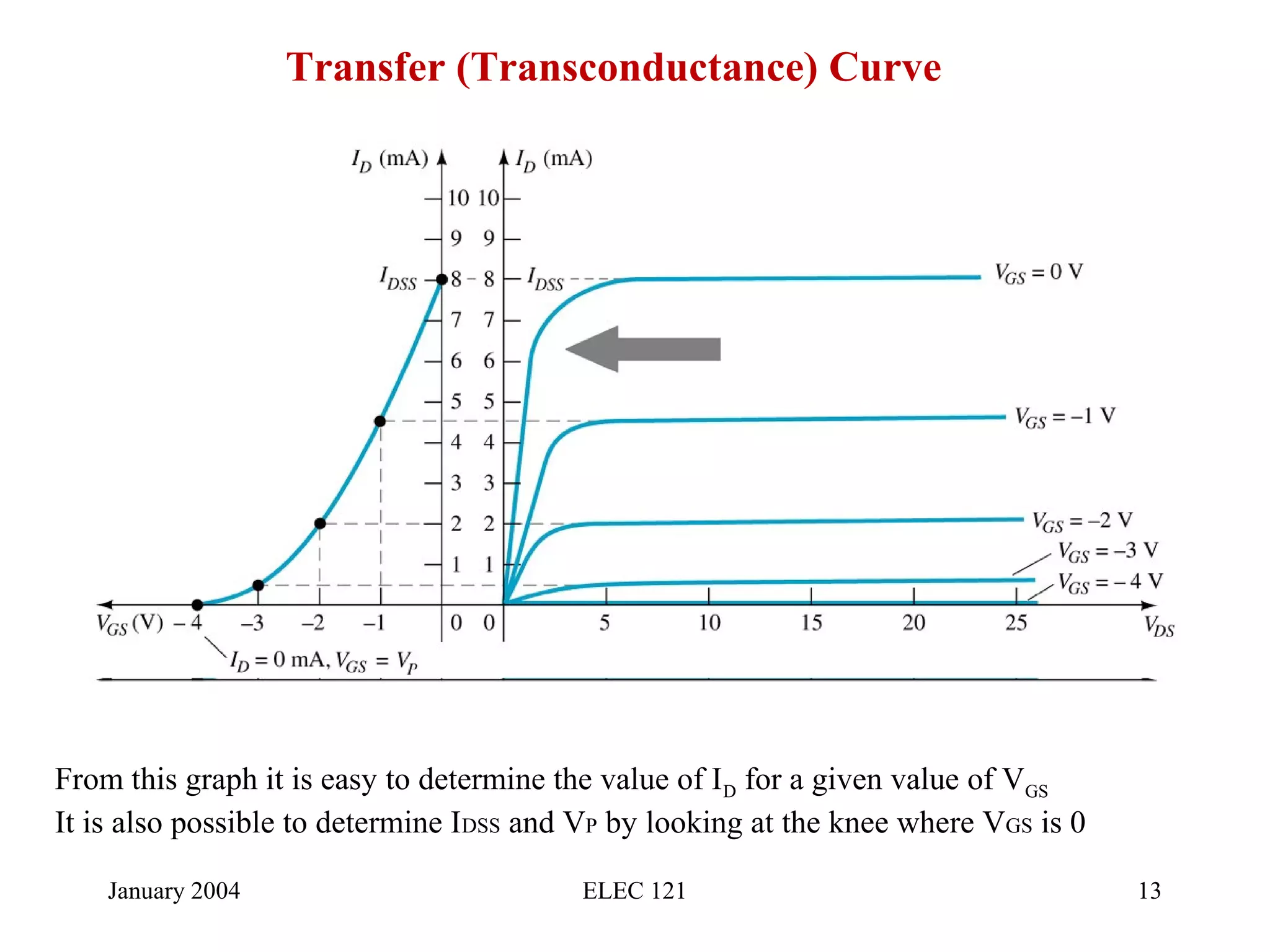
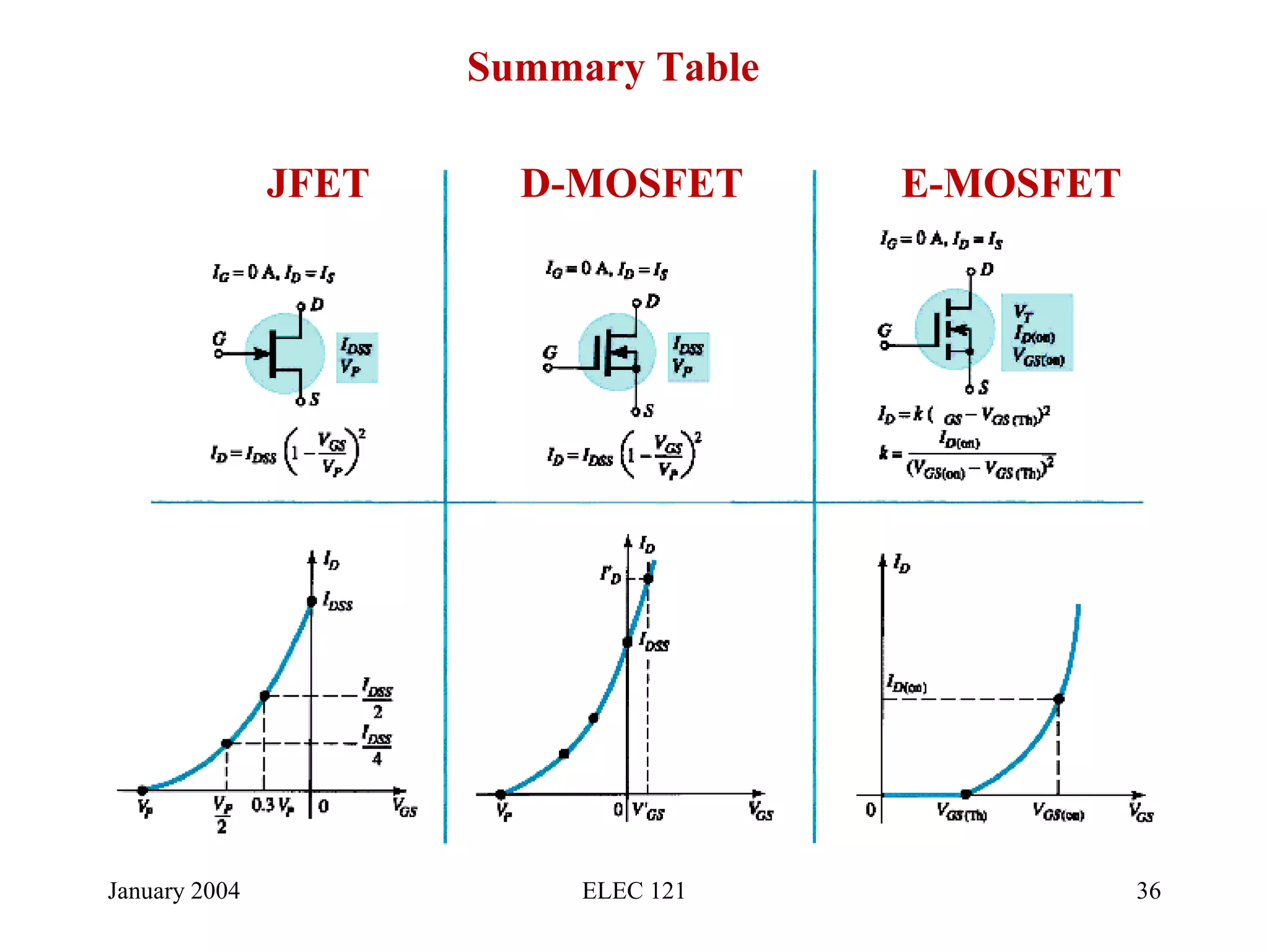
The document discusses different types of field effect transistors (FETs), including:
1) Junction FETs (JFETs), which operate in depletion mode only and have a non-linear relationship between input voltage and output current.
2) Depletion-mode metal-oxide-semiconductor FETs (D-MOSFETs), which can operate in either depletion or enhancement mode.
3) Enhancement-mode MOSFETs (E-MOSFETs), which only operate in enhancement mode and have an output current of zero until the input voltage exceeds the threshold voltage.
Concept of Field Effect Transistors (channel width modulation), Gate isolation types, JFET Structure and characteristics, MOSFET Structure and characteristics, depletion and enhancement type; CS, CG, CD configurations; CMOS: Basic Principles
The three terminals of the FET are known as Gate, Drain, and Source.
It is a voltage controlled device, where the input voltage controls by the output current.
In FET current used to flow between the drain and the source terminal. And this current can be controlled by applying the voltage between the gate and the source terminal.
So this applied voltage generate the electric field within the device and by controlling these electric field we can control the flow of current through the device.
Field Effect Transistor is a transistor that is voltage controlled devices. It has higher input impedance and less sensitive to temperature variations.
The MOSFET is an important element in embedded system design which is used to control the loads as per the requirement. The MOSFET is a high voltage controlling device provides some key features for circuit designers in terms of their overall performance.
SHORT-CHANNEL EFFECTS
A MOSFET is considered to be short when the channel length ‘L’ is the same order of magnitude as the depletion-layer widths (xdD, xdS). The potential distribution in the channel now depends upon both, transverse field Ex, due to gate bias and also on the longitudinal field Ey, due to drain bias When the Gate channel length <<1 m, short channel effect becomes important .
This leads to many
undesirable effects in MOSFET.
The short-channel effects are attributed to two physical phenomena:
A) The limitation imposed on electron drift characteristics in the channel,
B) The modification of the threshold voltage due to the shortening channel length.
In particular five different short-channel effects can be distinguished:
1. Drain-induced barrier lowering and “Punch through”
2. Surface scattering
3. Velocity saturation
4. Impact ionization
5. Hot electrons
The presentation covers, Field Effect Transistor: Construction and Characteristic of JFETs, dc biasing of CS, ac analysis of CS amplifier, MOSFET (Depletion and Enhancement)Type, Transfer Characteristic
A field-effect transistor (FET) is a type of transistor commonly used for weak-signal amplification (for example, for amplifying wireless signals). The device can amplify analog or digital signals. It can also switch DC or function as an oscillator.
The metal–oxide–semiconductor field-effect transistor (MOSFET, MOS-FET, or MOS FET) is a type of field-effect transistor (FET). It has an insulated gate, whose voltage determines the conductivity of the device. This ability to change conductivity with the amount of applied voltage can be used for amplifying or switching electronic signals. Although FET is sometimes used when referring to MOSFET devices, other types of field-effect transistors also exist.
Mosfet
MOSFETs have characteristics similar to JFETs and additional characteristics that make them very useful.
There are 2 types:
• Depletion-Type MOSFET
• Enhancement-Type MOSFET
Introduction to AI for Nonprofits with Tapp NetworkTechSoup
Dive into the world of AI! Experts Jon Hill and Tareq Monaur will guide you through AI's role in enhancing nonprofit websites and basic marketing strategies, making it easy to understand and apply.
Honest Reviews of Tim Han LMA Course Program.pptxtimhan337
Personal development courses are widely available today, with each one promising life-changing outcomes. Tim Han’s Life Mastery Achievers (LMA) Course has drawn a lot of interest. In addition to offering my frank assessment of Success Insider’s LMA Course, this piece examines the course’s effects via a variety of Tim Han LMA course reviews and Success Insider comments.
Read| The latest issue of The Challenger is here! We are thrilled to announce that our school paper has qualified for the NATIONAL SCHOOLS PRESS CONFERENCE (NSPC) 2024. Thank you for your unwavering support and trust. Dive into the stories that made us stand out!
Operation “Blue Star” is the only event in the history of Independent India where the state went into war with its own people. Even after about 40 years it is not clear if it was culmination of states anger over people of the region, a political game of power or start of dictatorial chapter in the democratic setup.
The people of Punjab felt alienated from main stream due to denial of their just demands during a long democratic struggle since independence. As it happen all over the word, it led to militant struggle with great loss of lives of military, police and civilian personnel. Killing of Indira Gandhi and massacre of innocent Sikhs in Delhi and other India cities was also associated with this movement.
Francesca Gottschalk - How can education support child empowerment.pptxEduSkills OECD
Francesca Gottschalk from the OECD’s Centre for Educational Research and Innovation presents at the Ask an Expert Webinar: How can education support child empowerment?
Welcome to TechSoup New Member Orientation and Q&A (May 2024).pdfTechSoup
In this webinar you will learn how your organization can access TechSoup's wide variety of product discount and donation programs. From hardware to software, we'll give you a tour of the tools available to help your nonprofit with productivity, collaboration, financial management, donor tracking, security, and more.
The French Revolution, which began in 1789, was a period of radical social and political upheaval in France. It marked the decline of absolute monarchies, the rise of secular and democratic republics, and the eventual rise of Napoleon Bonaparte. This revolutionary period is crucial in understanding the transition from feudalism to modernity in Europe.
For more information, visit-www.vavaclasses.com
A Strategic Approach: GenAI in EducationPeter Windle
Artificial Intelligence (AI) technologies such as Generative AI, Image Generators and Large Language Models have had a dramatic impact on teaching, learning and assessment over the past 18 months. The most immediate threat AI posed was to Academic Integrity with Higher Education Institutes (HEIs) focusing their efforts on combating the use of GenAI in assessment. Guidelines were developed for staff and students, policies put in place too. Innovative educators have forged paths in the use of Generative AI for teaching, learning and assessments leading to pockets of transformation springing up across HEIs, often with little or no top-down guidance, support or direction.
This Gasta posits a strategic approach to integrating AI into HEIs to prepare staff, students and the curriculum for an evolving world and workplace. We will highlight the advantages of working with these technologies beyond the realm of teaching, learning and assessment by considering prompt engineering skills, industry impact, curriculum changes, and the need for staff upskilling. In contrast, not engaging strategically with Generative AI poses risks, including falling behind peers, missed opportunities and failing to ensure our graduates remain employable. The rapid evolution of AI technologies necessitates a proactive and strategic approach if we are to remain relevant.
2. January 2004 ELEC 121 2
Current Controlled vs Voltage Controlled Devices
3. January 2004 ELEC 121 3
• JFET – Junction Field Effect Transistor
• MOSFET – Metal Oxide Semiconductor Field Effect
Transistor
– D-MOSFET - Depletion Mode MOSFET
– E- MOSFET - Enhancement Mode MOSFET
Types of FET’s
4. January 2004 ELEC 121 4
Transfer Characteristics
The input-output transfer characteristic of the JFET is not as straight
forward as it is for the BJT
In a BJT, β (hFE) defined the relationship between IB (input current) and IC
(output current).
In a JFET, the relationship (Shockley’s Equation) between VGS (input
voltage) and ID (output current) is used to define the transfer characteristics,
and a little more complicated (and not linear):
As a result, FET’s are often referred to a square law devices
÷
2
GS
D DSS
P
V
I = I 1-
V
5. January 2004 ELEC 121 5
JFET Construction
There are two types of JFET’s: n-channel and p-channel.
The n-channel is more widely used.
There are three terminals: Drain (D) and Source (S) are connected to n-channel
Gate (G) is connected to the p-type material
6. January 2004 ELEC 121 6
JFET Operating Characteristics
There are three basic operating conditions for a JFET:
JFET’s operate in the depletion mode only
A. VGS = 0, VDS is a minimum value depending on IDSS and the
drain and source resistance
B. VGS < 0, VDS at some positive value and
C. Device is operating as a Voltage-Controlled Resistor
For an n channel JFET, VGS may never be positive*
For an p channel JFET, VGS may never be negative*
8. January 2004 ELEC 121 8
The nonconductive depletion region becomes thicker with increased reverse bias.
(Note: The two gate regions of each FET are connected to each other.)
N-Channel JFET Operation
10. January 2004 ELEC 121 10
Saturation
At the pinch-off point:
• any further increase in VGS does not produce any increase in ID. VGS at
pinch-off is denoted as Vp.
• ID is at saturation or maximum. It is referred to as IDSS.
• The ohmic value of the channel is at maximum.
11. January 2004 ELEC 121 11
ID ≤ IDSS
As VGS becomes more negative:
• the JFET will pinch-off at a lower voltage (Vp).
• ID decreases (ID < IDSS) even though VDS is increased.
• Eventually ID will reach 0A. VGS at this point is called Vp or VGS(off).
• Also note that at high levels of VDS the JFET reaches a breakdown situation.
ID will increases uncontrollably if VDS > VDSmax.
12. January 2004 ELEC 121 12
FET as a Voltage-Controlled Resistor
The region to the left of the pinch-off point is called the ohmic
region.
The JFET can be used as a variable resistor, where VGS controls
the drain-source resistance (rd). As VGS becomes more negative,
the resistance (rd) increases.
÷
o
d
2
GS
P
r
r =
V
1-
V
13. January 2004 ELEC 121 13
Transfer (Transconductance) Curve
From this graph it is easy to determine the value of ID for a given value of VGS
It is also possible to determine IDSS and VP by looking at the knee where VGS is 0
14. January 2004 ELEC 121 14
Plotting the Transconductance Curve
Using IDSS and VP (or VGS(off)) values found in a specification sheet, the Family of Curves
can be plotted by making a table of data using the following 3 steps:
Step 1:
Solve for VGS = 0V
Step 2
Solve for VGS = VP ( aka VGS(off) )
Step 3:
Solve for 0V ≥VGS ≥ VP in 1V increments for VGS
÷
2
GS
D DSS
P
V
I = I 1-
V
÷
2
GS
D DSS
P
V
I = I 1-
V
÷
2
GS
D DSS
P
V
I = I 1-
V
15. January 2004 ELEC 121 15
Case Construction and Terminal Identification
This information is found on the specification sheet
16. January 2004 ELEC 121 16
p-Channel JFET’s
p-Channel JFET operates in a similar manner as the n-channel JFET except the voltage
polarities and current directions are reversed
17. January 2004 ELEC 121 17
P-Channel JFET Characteristics
As VGS increases more positively
• the depletion zone increases
• ID decreases (ID < IDSS)
• eventually ID = 0A
Also note that at high levels of VDS the JFET reaches a breakdown situation. ID
increases uncontrollably if VDS > VDSmax.
19. January 2004 ELEC 121 19
MOSFETs
MOSFETs have characteristics similar to JFETs and additional
characteristics that make then very useful
There are 2 types of MOSFET’s:
• Depletion mode MOSFET (D-MOSFET)
• Operates in Depletion mode the same way as a JFET when VGS ≤ 0
• Operates in Enhancement mode like E-MOSFET when VGS > 0
• Enhancement Mode MOSFET (E-MOSFET)
• Operates in Enhancement mode
• IDSS = 0 until VGS > VT (threshold voltage)
20. January 2004 ELEC 121 20
MOSFET Handling
MOSFETs are very static sensitive. Because of the very thin SiO2 layer
between the external terminals and the layers of the device, any small electrical
discharge can stablish an unwanted conduction.
Protection:
• Always transport in a static sensitive bag
• Always wear a static strap when handling MOSFETS
• Apply voltage limiting devices between the Gate and Source, such as back-to-
back Zeners to limit any transient voltage
23. January 2004 ELEC 121 23
Depletion Mode MOSFET Construction
The Drain (D) and Source (S) leads connect to the to n-doped regions
These N-doped regions are connected via an n-channel
This n-channel is connected to the Gate (G) via a thin insulating layer of SiO2
The n-doped material lies on a p-doped substrate that may have an additional terminal
connection called SS
24. January 2004 ELEC 121 24
Basic Operation
A D-MOSFET may be biased to operate in two modes:
the Depletion mode or the Enhancement mode
25. January 2004 ELEC 121 25
D-MOSFET Depletion Mode Operation
The transfer characteristics are similar to the JFET
In Depletion Mode operation:
When VGS = 0V, ID = IDSS
When VGS < 0V, ID < IDSS
When VGS > 0V, ID > IDSS
The formula used to plot the Transfer Curve, is:
÷
2
GS
D DSS
P
V
I = I 1-
V
26. January 2004 ELEC 121 26
D-MOSFET Enhancement Mode Operation
Enhancement Mode operation
In this mode, the transistor operates with VGS > 0V, and ID increases above IDSS
Shockley’s equation, the formula used to plot the Transfer Curve, still applies but VGS is
positive:
÷
2
GS
D DSS
P
V
I = I 1-
V
27. January 2004 ELEC 121 27
p-Channel Depletion Mode MOSFET
The p-channel Depletion mode MOSFET is similar to the n-channel except that the
voltage polarities and current directions are reversed
29. January 2004 ELEC 121 29
n-Channel E-MOSFET showing channel length L and
channel width W
30. January 2004 ELEC 121 30
Enhancement Mode MOSFET Construction
The Drain (D) and Source (S) connect to the to n-doped regions
These n-doped regions are not connected via an n-channel without an external voltage
The Gate (G) connects to the p-doped substrate via a thin insulating layer of SiO2
The n-doped material lies on a p-doped substrate that may have an additional terminal
connection called SS
33. January 2004 ELEC 121 33
Basic Operation
The Enhancement mode MOSFET only operates in the enhancement mode.
VGS is always positive
IDSS = 0 when VGS < VT
As VGS increases above VT, ID increases
If VGS is kept constant and VDS is increased, then ID saturates (IDSS)
The saturation level, VDSsat is reached.
34. January 2004 ELEC 121 34
Transfer Curve
To determine ID given VGS:
where VT = threshold voltage or voltage at which the MOSFET turns on.
k = constant found in the specification sheet
The PSpice determination of k is based on the geometry of the device:
2
D GS TI = k (V - V )
D(on)
2
GS(ON) T
I
k =
(V - V )
÷ ÷
N OX
W KP
k = where KP = μ C
L 2
35. January 2004 ELEC 121 35
p-Channel Enhancement Mode MOSFETs
The p-channel Enhancement mode MOSFET is similar to the n-channel except that the
voltage polarities and current directions are reversed.