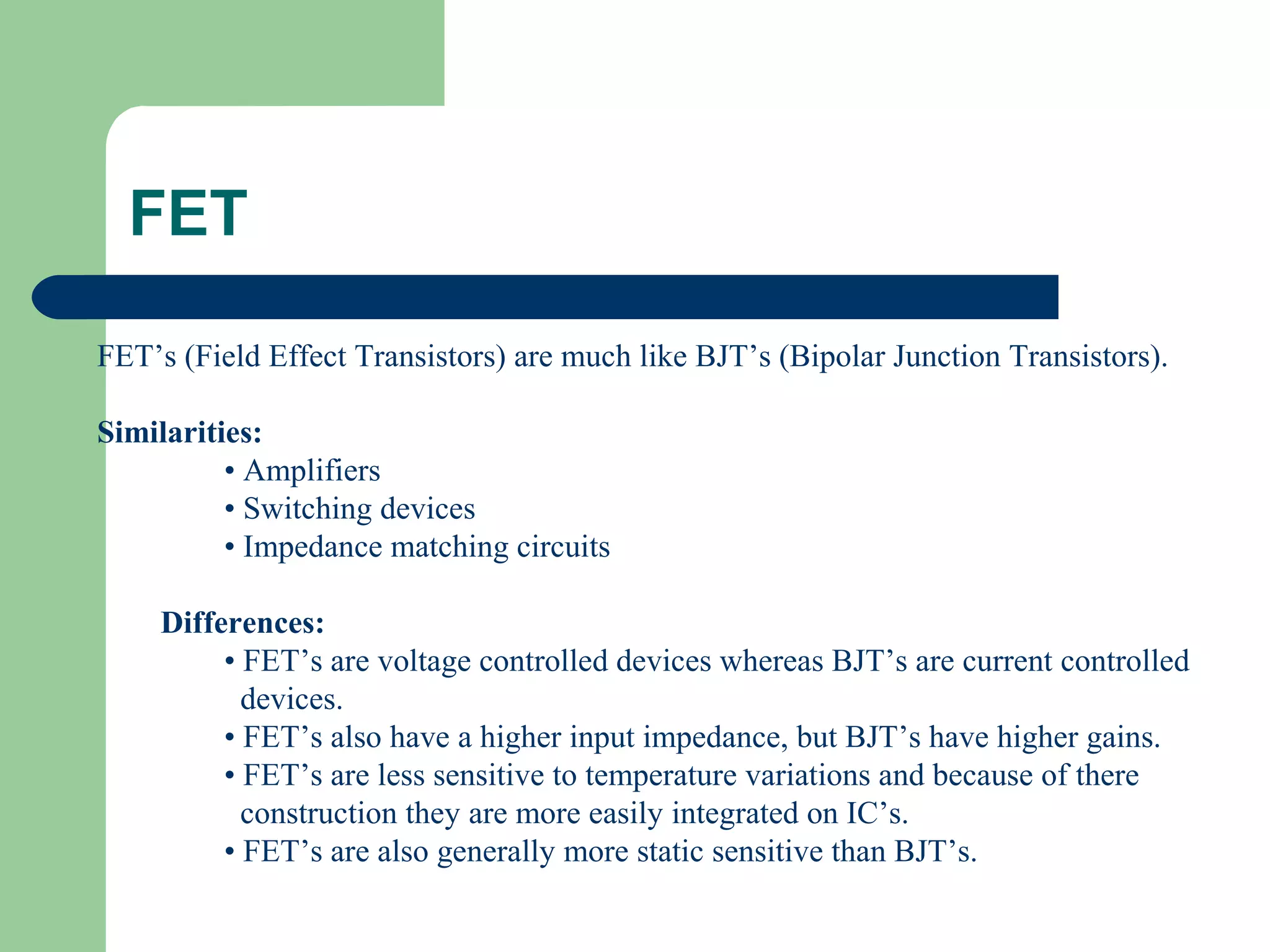
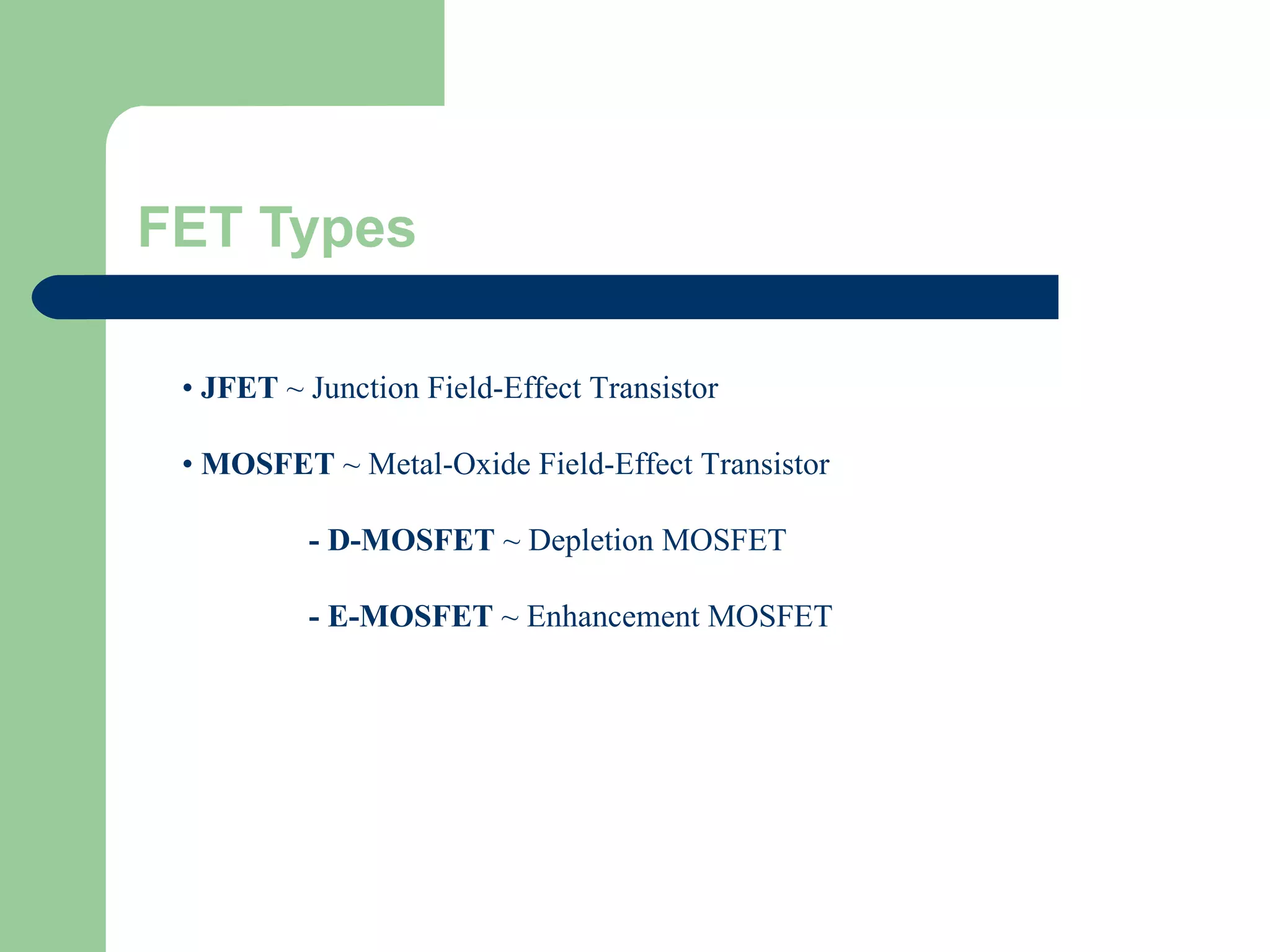
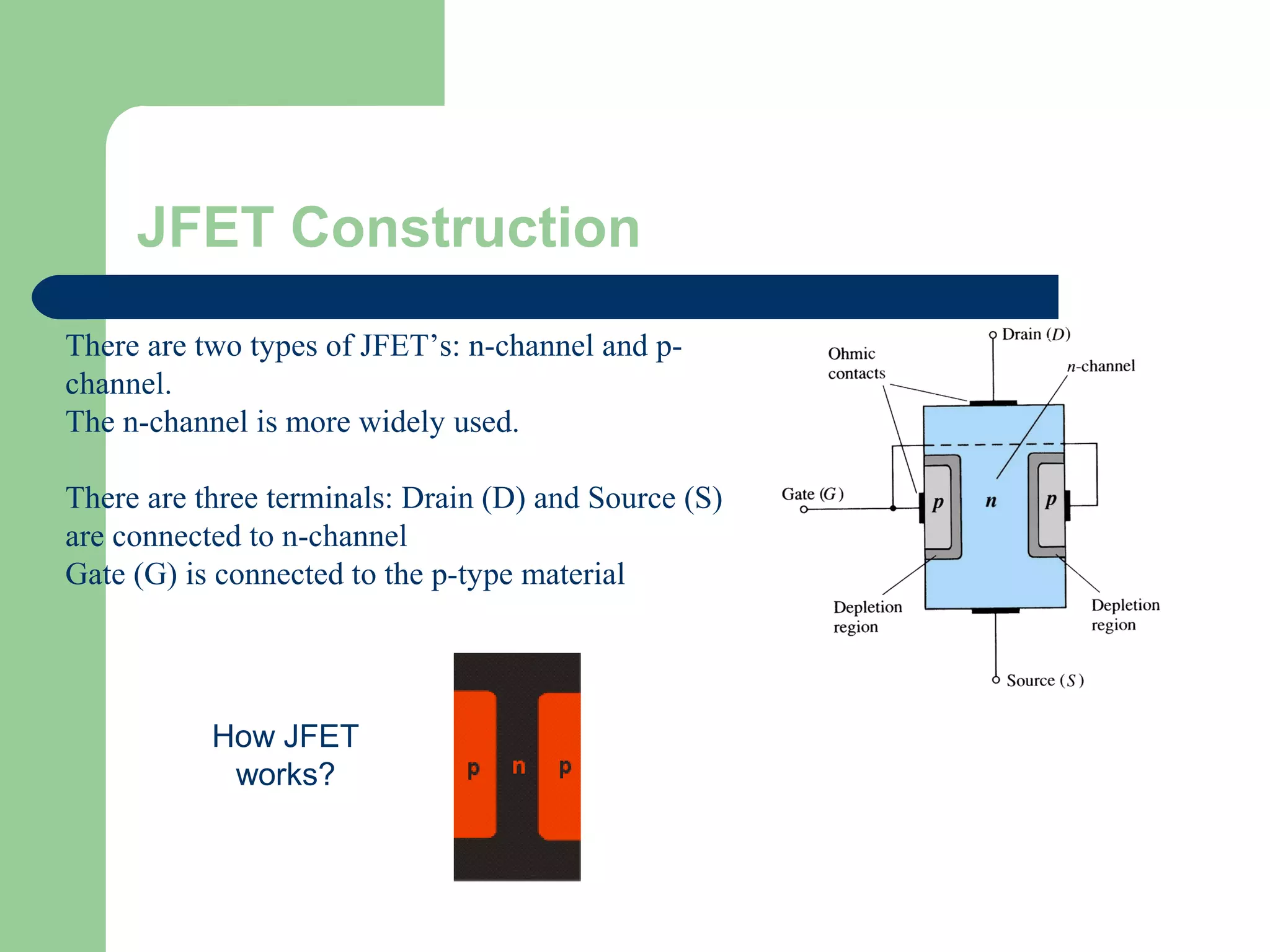
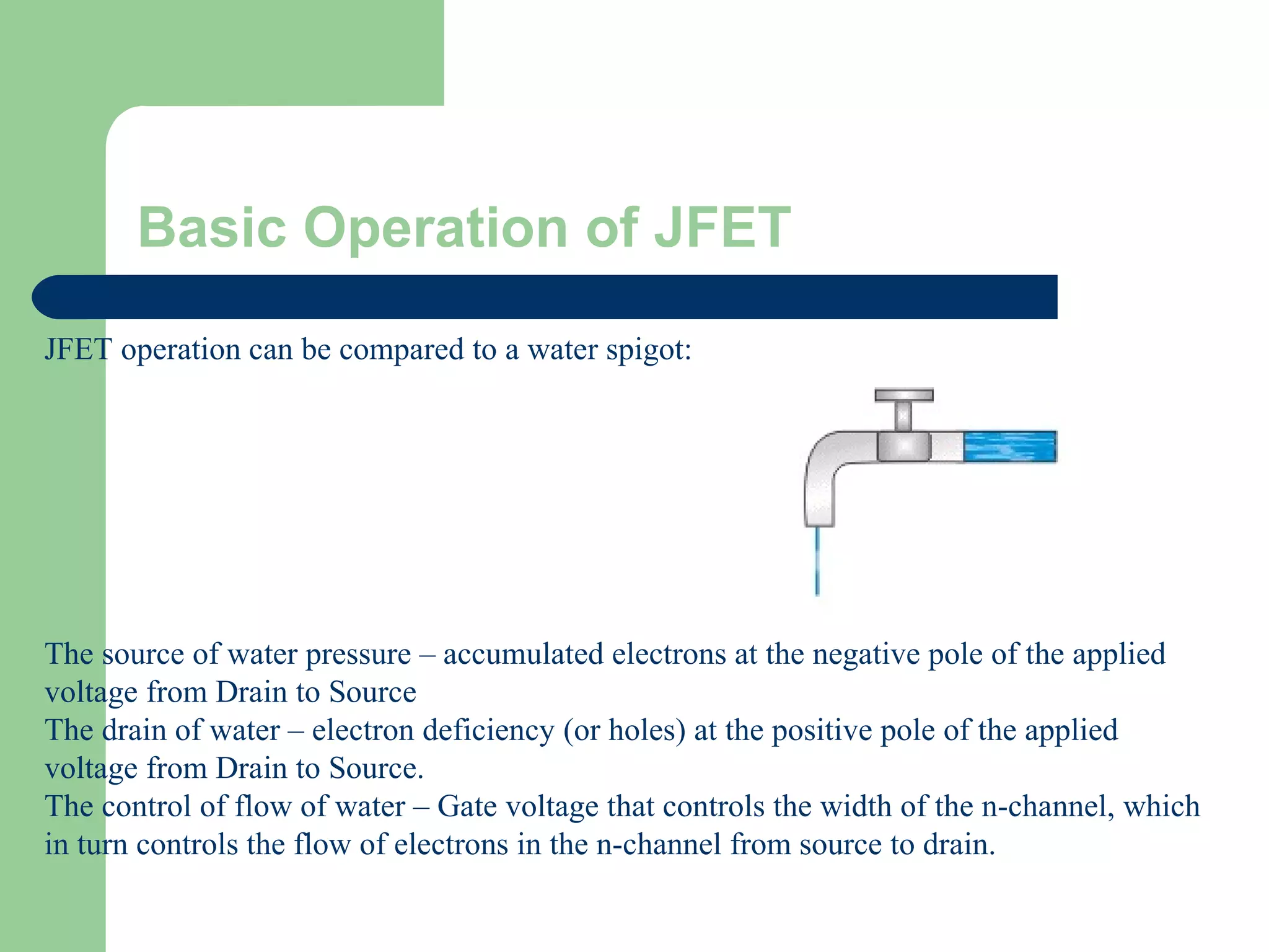
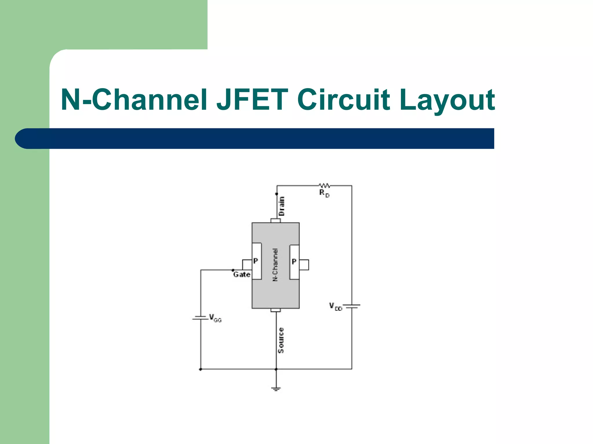
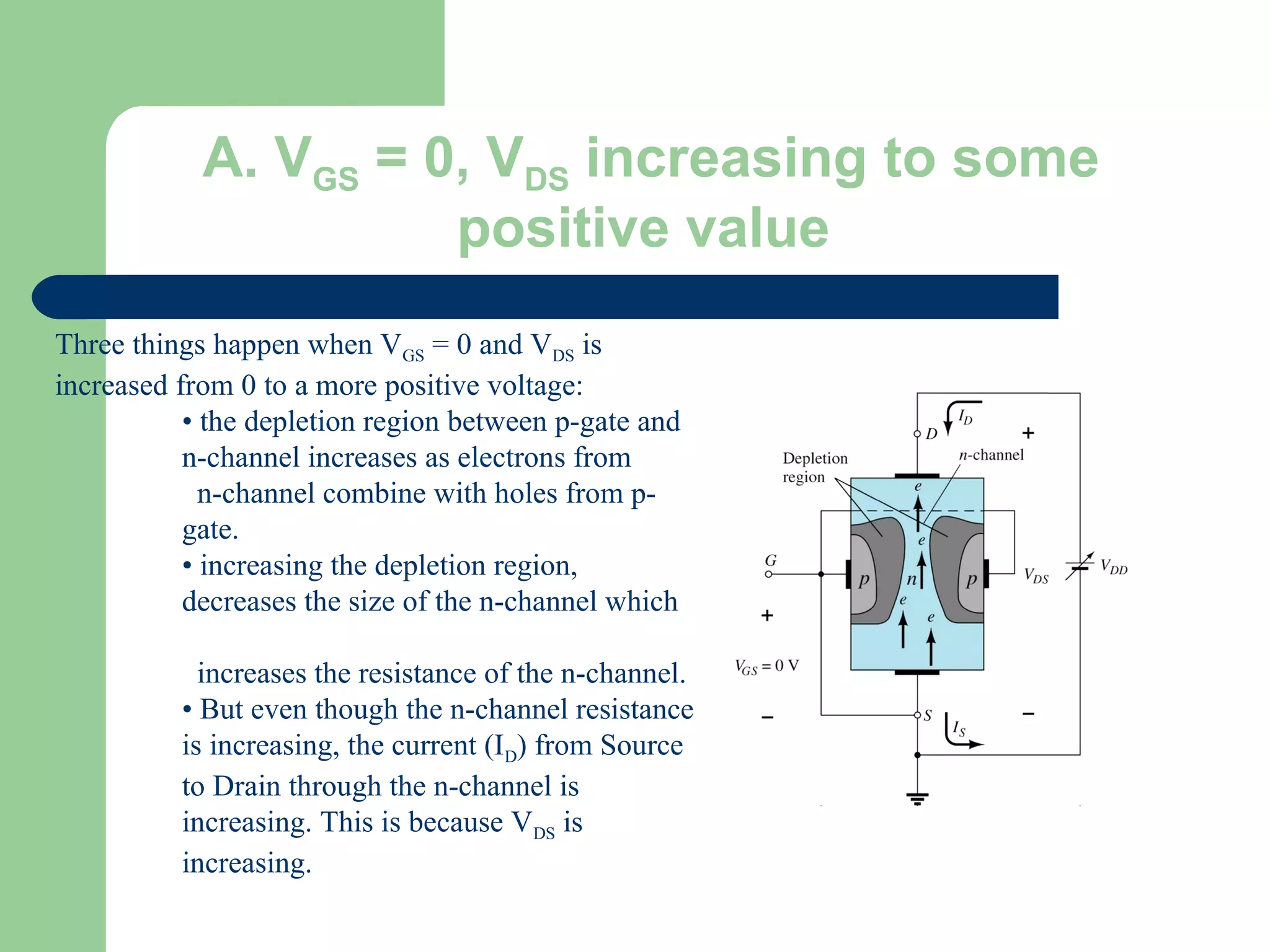
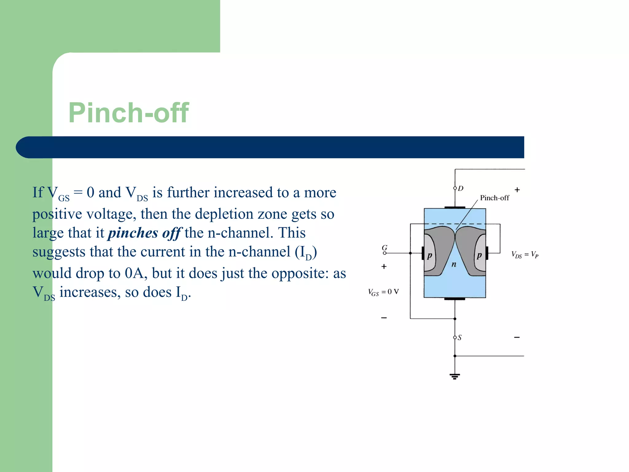
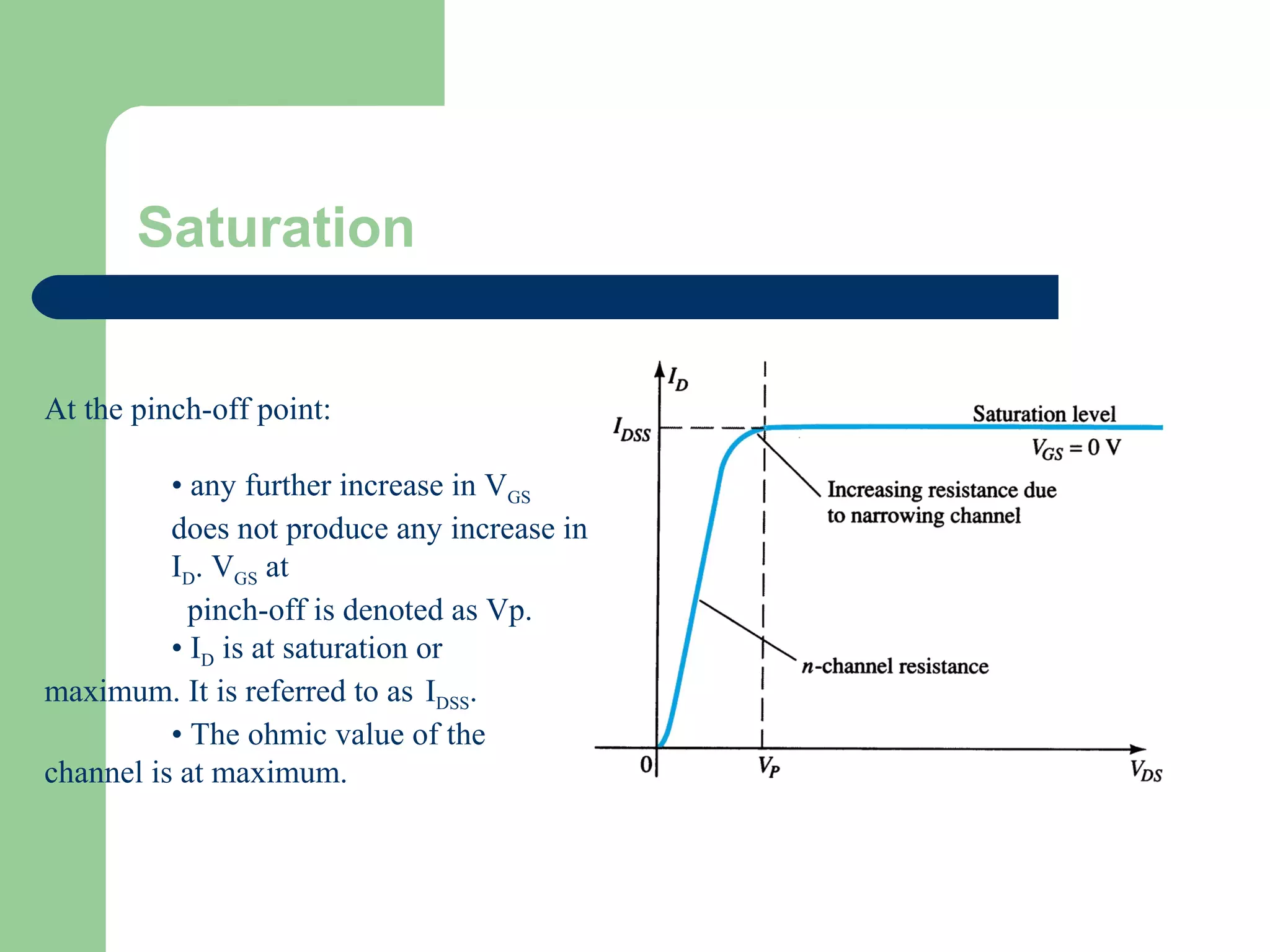
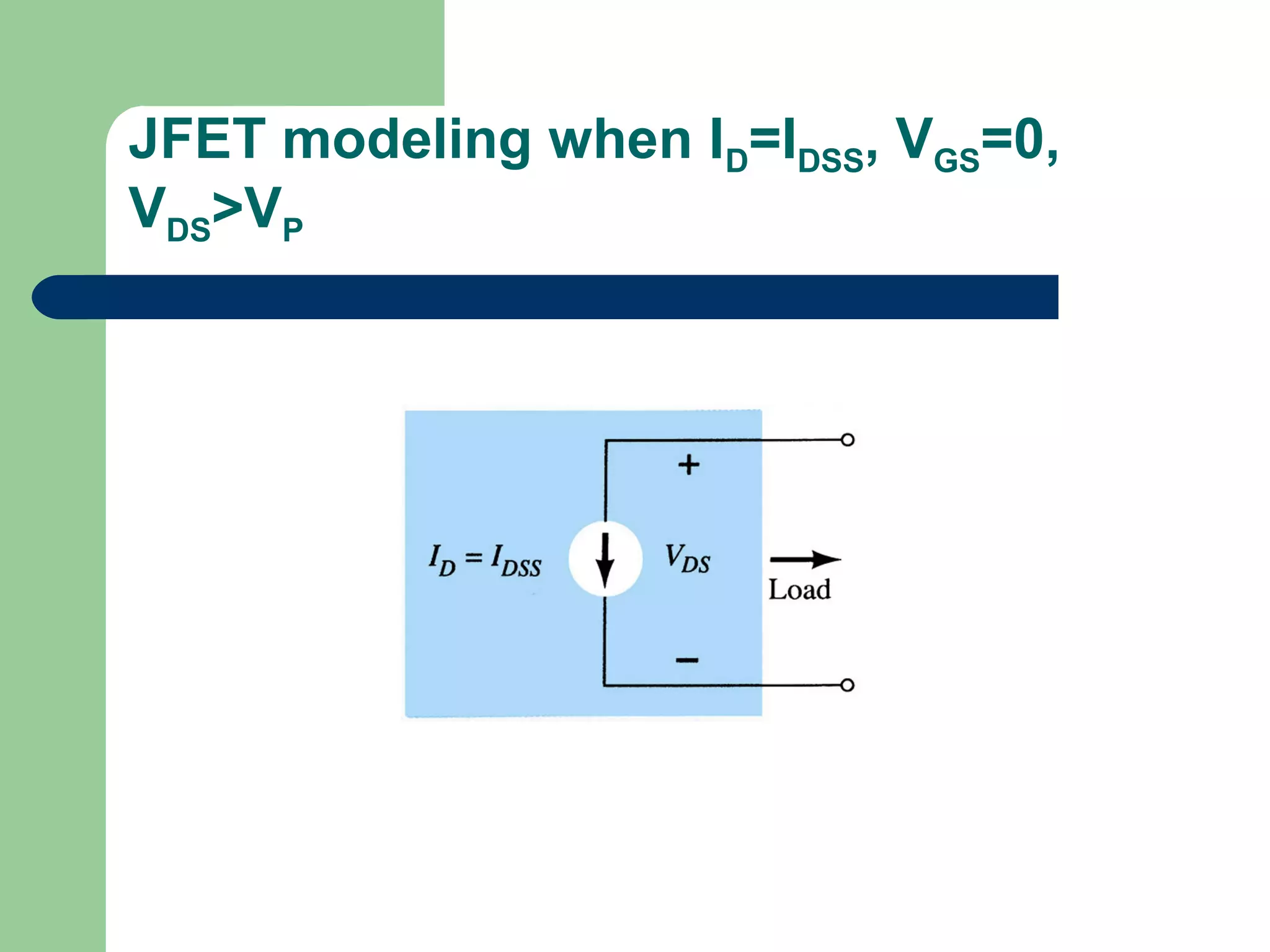
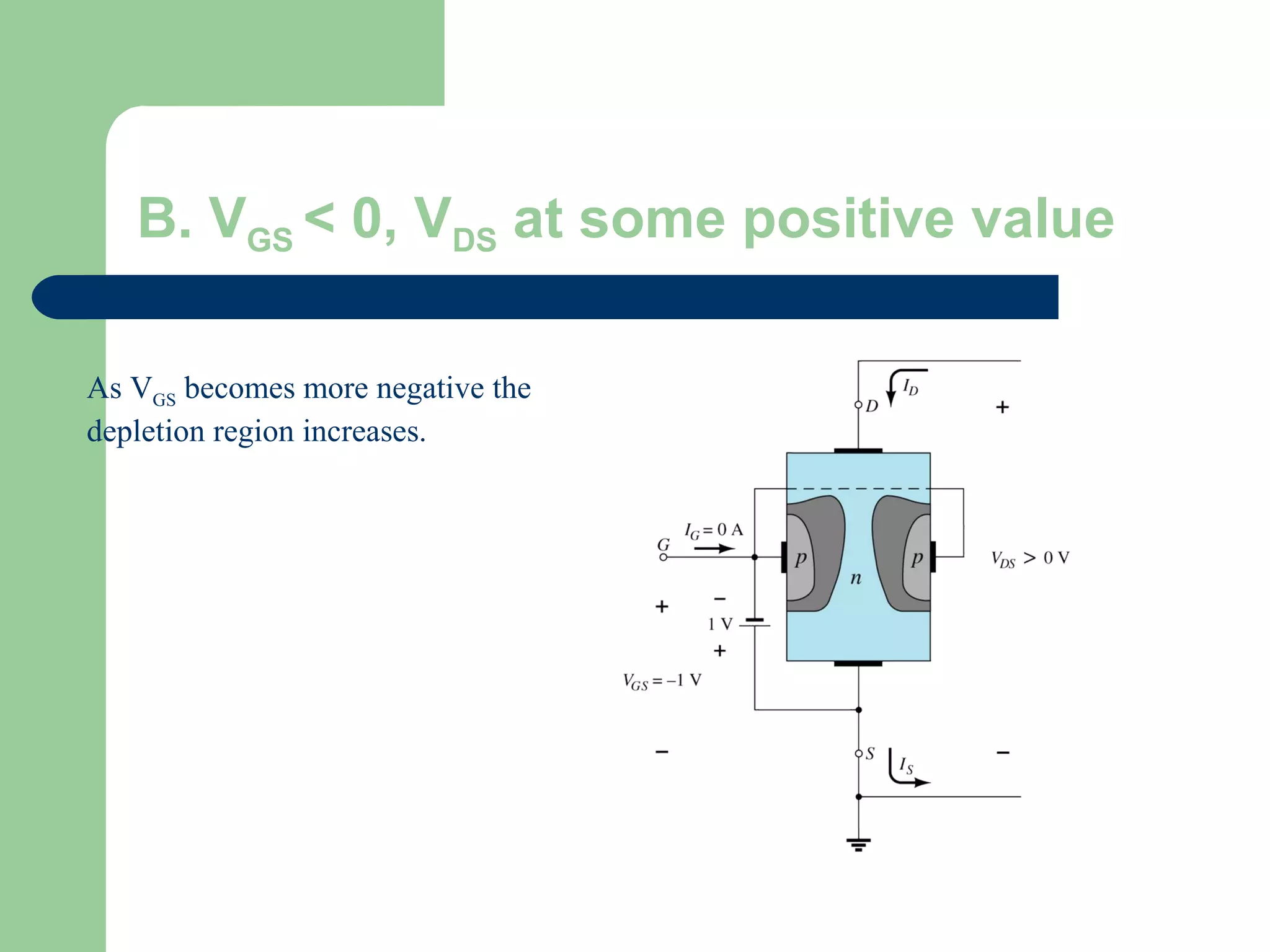
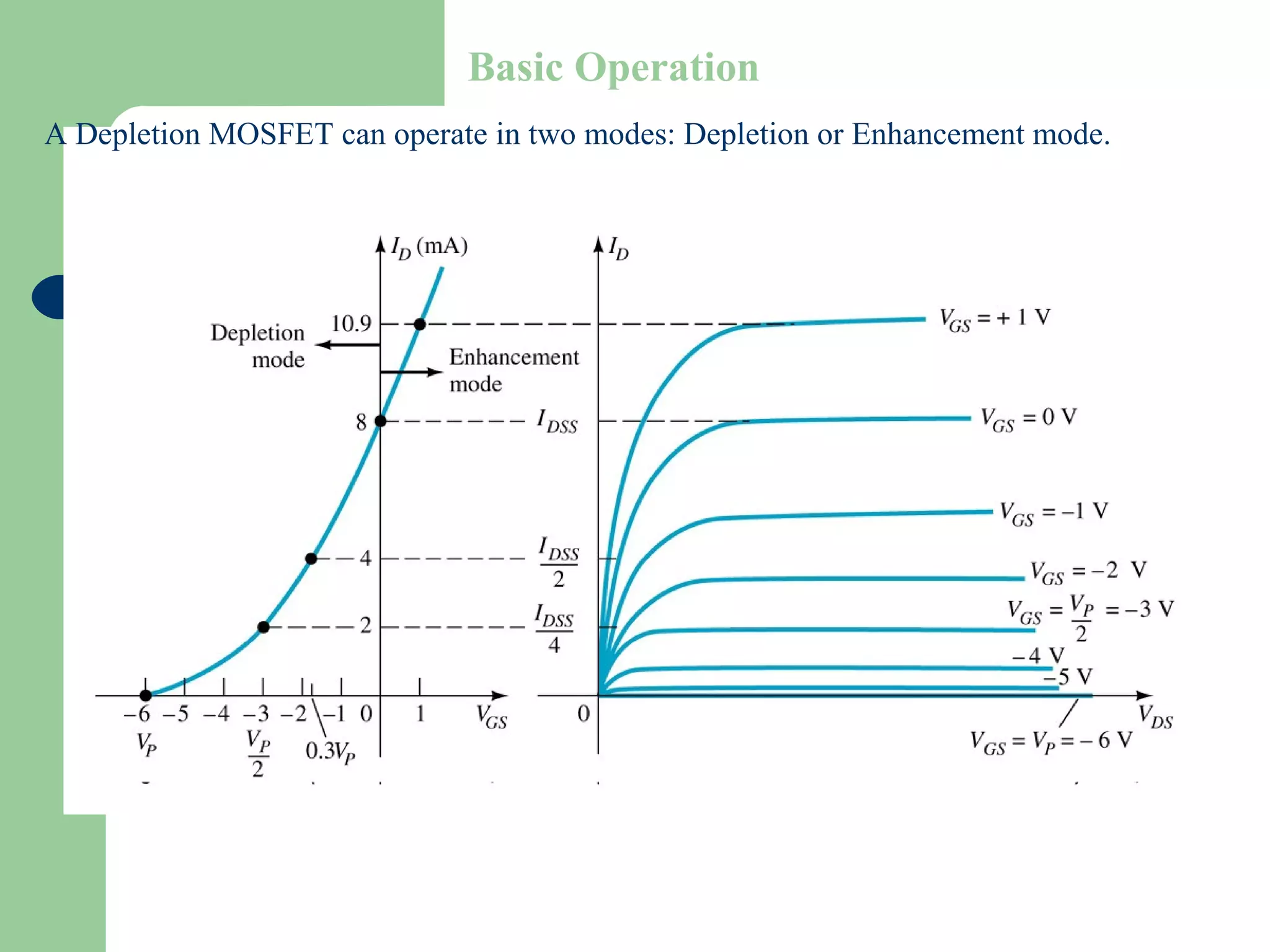
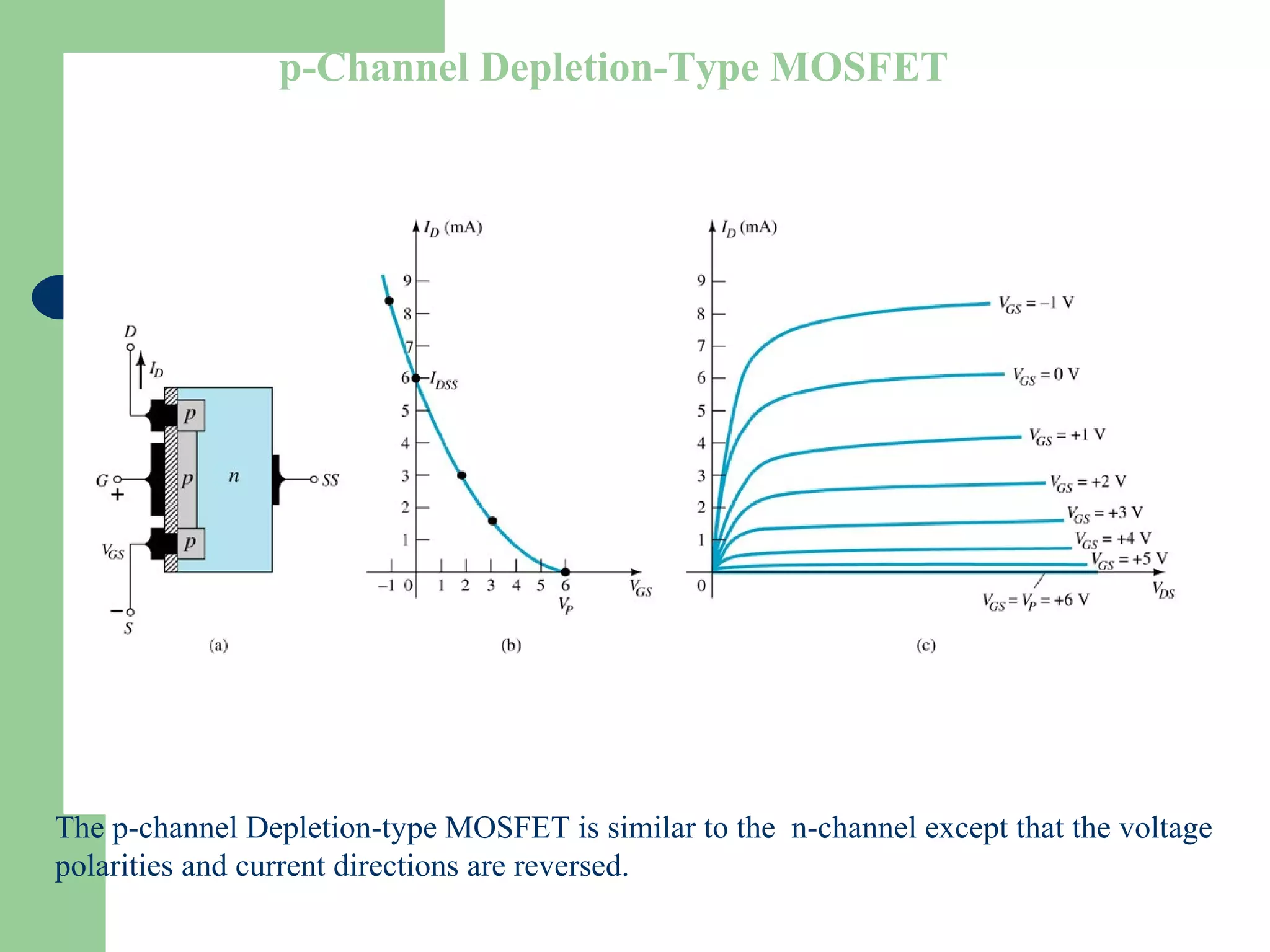
The document discusses different types of field effect transistors (FETs), including JFETs and MOSFETs. It explains the construction, operation, and characteristics of n-channel JFETs and describes how to plot their transfer and drain characteristics. It also covers depletion-type and enhancement-type MOSFETs, discussing their construction, modes of operation, and how to plot their transfer curves. Key aspects like threshold voltage and methods of testing FETs are also summarized.

![Depletion-type MOSFET in Depletion Mode
Depletion mode
The characteristics are similar to the JFET.
When VGS = 0V, ID = IDSS
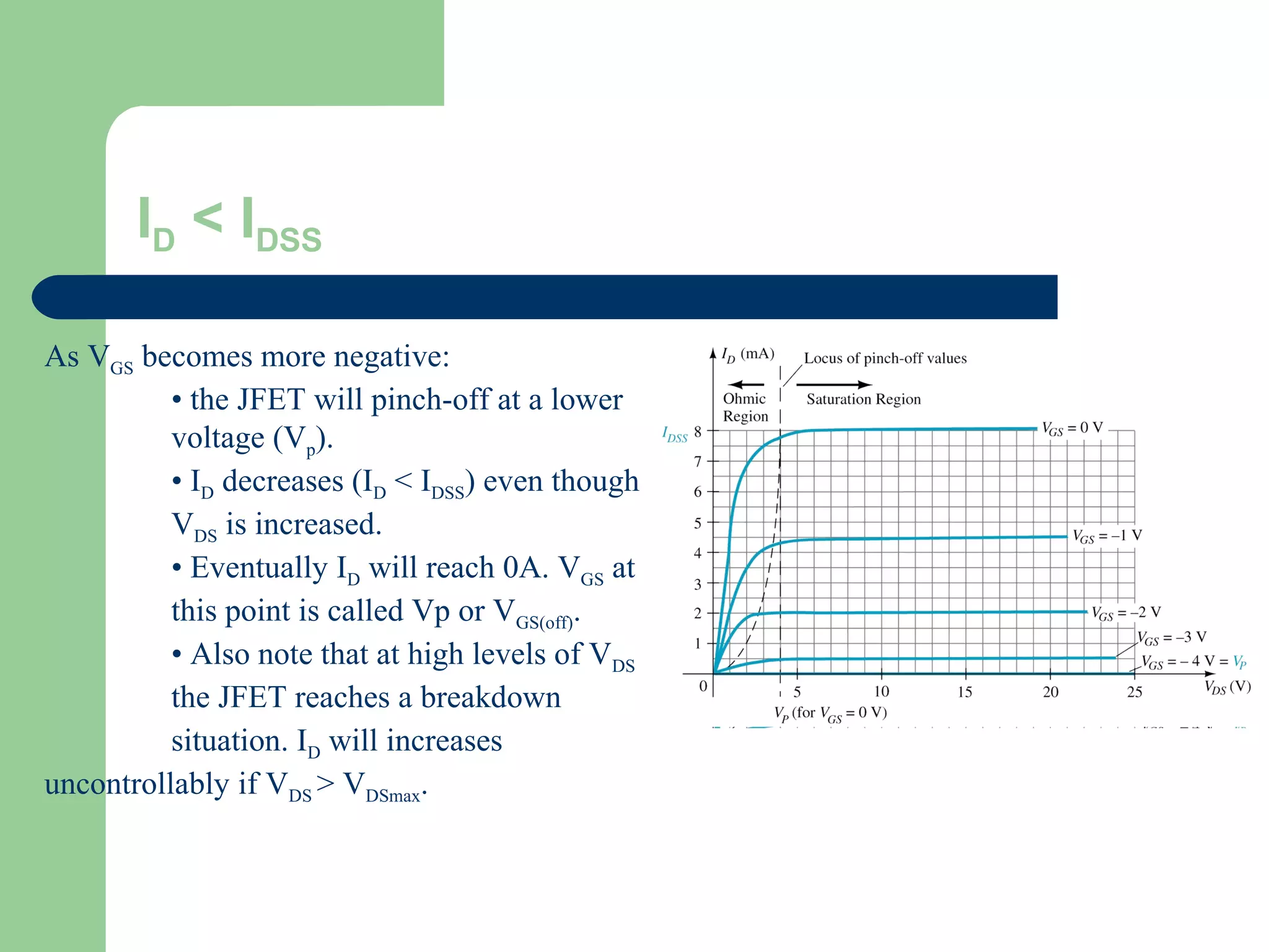
When VGS < 0V, ID < IDSS
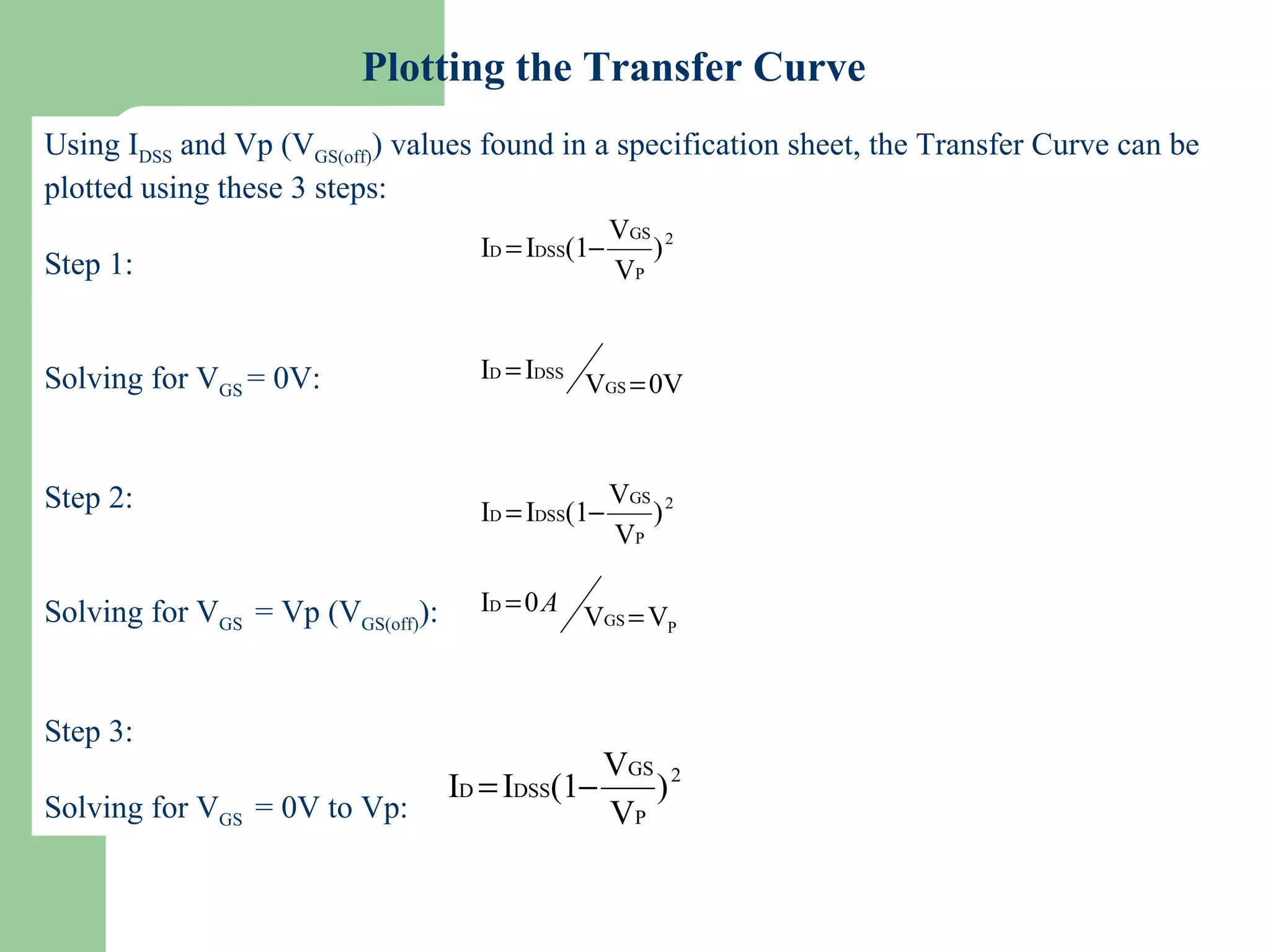
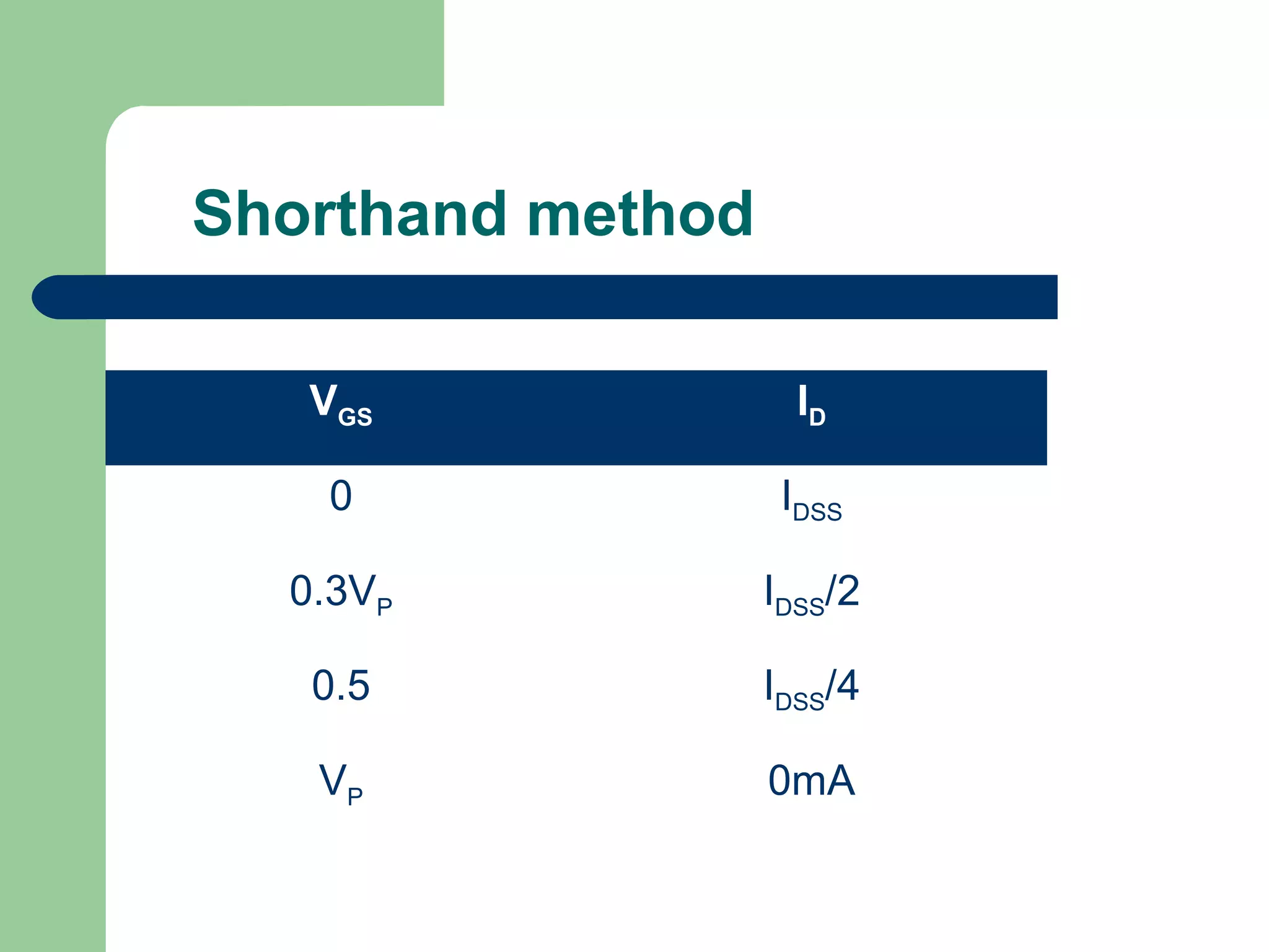
The formula used to plot the Transfer Curve still applies:
[Formula 5.3]2
P
GS
DSSD )
V
V
(1II −=](https://image.slidesharecdn.com/fetlecturefor08batch2010-161026192714/75/FET-lecture_Electronics-by-Arif-Sir-31-2048.jpg)
![Depletion-type MOSFET in Enhancement Mode
Enhancement mode
VGS > 0V, ID increases above IDSS
The formula used to plot the
Transfer Curve still applies: [Formula 5.3]
(note that VGS is now a positive polarity)
2
P
GS
DSSD )
V
V
(1II −=](https://image.slidesharecdn.com/fetlecturefor08batch2010-161026192714/75/FET-lecture_Electronics-by-Arif-Sir-32-2048.jpg)
![Slide 30
Basic Operation
The Enhancement-type MOSFET only operates in the enhancement mode.
VGS is always positive
As VGS increases, ID increases
But if VGS is kept constant and VDS is increased, then ID saturates (IDSS)
The saturation level, VDSsat is reached.
[Formula 5.12]
TGSDsat VVV −=](https://image.slidesharecdn.com/fetlecturefor08batch2010-161026192714/75/FET-lecture_Electronics-by-Arif-Sir-39-2048.jpg)
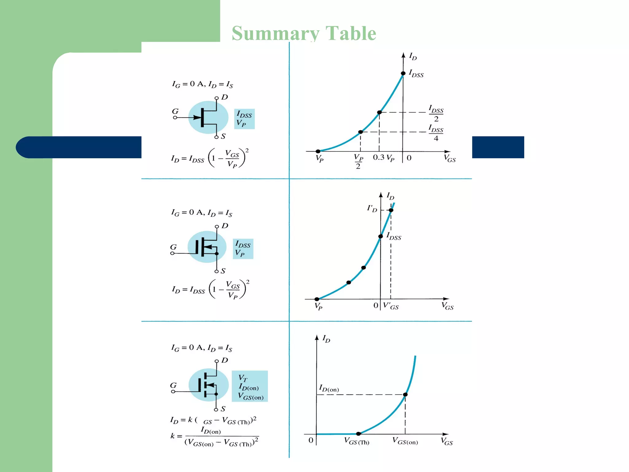
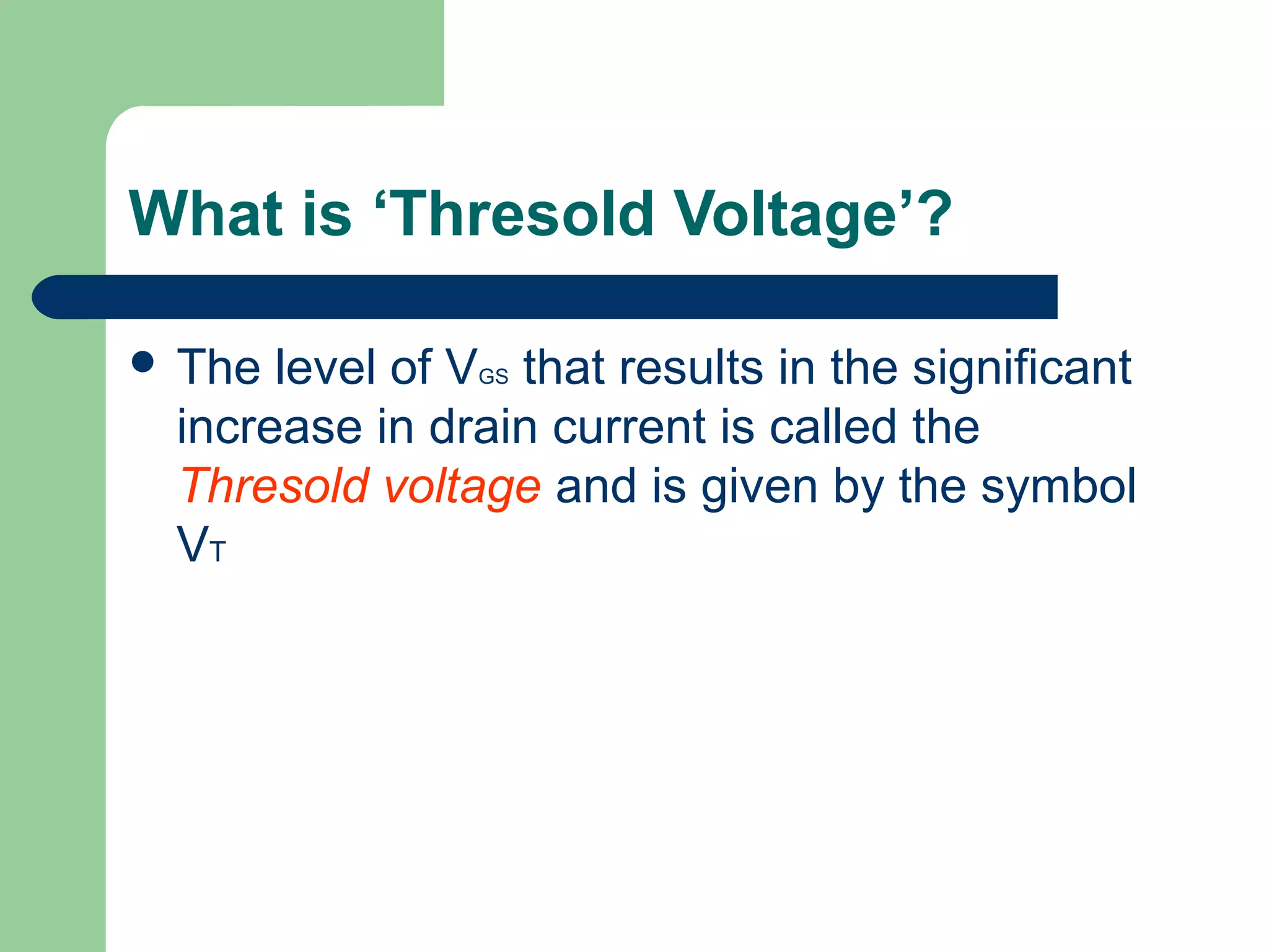
![Transfer Curve
To determine ID given VGS: [Formula 5.13]
where VT = threshold voltage or voltage at which the MOSFET turns on.
k = constant found in the specification sheet
k can also be determined by using values at a specific point and the formula:
[Formula 5.14]
VDSsat can also be calculated:
[Formula 5.12]
2
)( TGSD VVkI −=
2
TGS(ON)
D(on)
)V(V
I
k
−
=
TGSDsat VVV −=](https://image.slidesharecdn.com/fetlecturefor08batch2010-161026192714/75/FET-lecture_Electronics-by-Arif-Sir-40-2048.jpg)