
Download to read offline

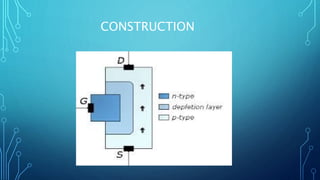
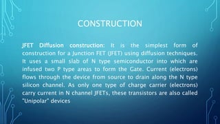
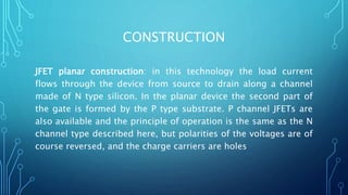
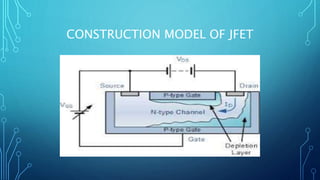
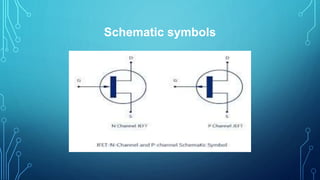
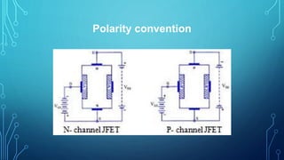

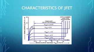


This document discusses the Junction Field Effect Transistor (JFET). It provides an introduction, explaining that a JFET is a three-terminal semiconductor device that can be used as a controlled switch, amplifier, or voltage-controlled resistor. It operates using the properties of a PN junction diode under forward and reverse bias. The document then discusses the construction of JFETs using diffusion and planar techniques, providing diagrams. It also covers the schematic symbol, polarity convention, and working principle of a JFET, comparing it to squeezing a garden hose to control water flow. Key characteristics and applications are summarized, along with the conclusion that JFETs are unipolar devices widely used as amplifiers with high input


![Aim-to study characterstics of fet (field effect [Autosaved].pptx](https://cdn.slidesharecdn.com/ss_thumbnails/aim-tostudycharactersticsoffetfieldeffectautosaved-221113041420-4dcee974-thumbnail.jpg?width=640&height=640&fit=bounds)


