Download to read offline


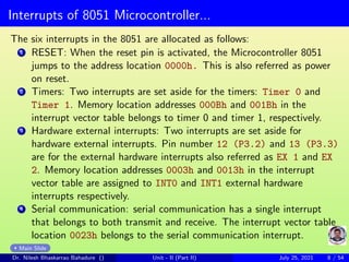
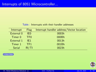


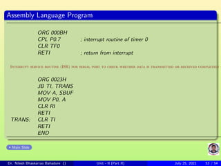


The document provides a comprehensive overview of interrupts in the 8051 microcontroller, detailing their types, functioning, and programming. It contrasts interrupts with polling, explaining the efficiency of interrupts in microcontroller operations, and includes examples for various interrupt scenarios. Additionally, it covers specific registers related to interrupts, such as the IE and IP registers, and discusses the procedural steps when an interrupt occurs or ends.