INTERFACING ANALAOG TO DIGITAL CONVERTER (ADC0808/09) TO 8051 MICROCONTROLLER
The document discusses interfacing an ADC IC0808/09 chip with a microcontroller. It describes how the ADC chip converts analog signals to digital signals using successive approximation. It explains the pinout, features and working of the ADC chip. It also discusses how to interface the ADC0809 chip with an 8051 microcontroller by selecting channels, initiating conversions and reading output data.
ADC INTERFACING USING
IC0808/09
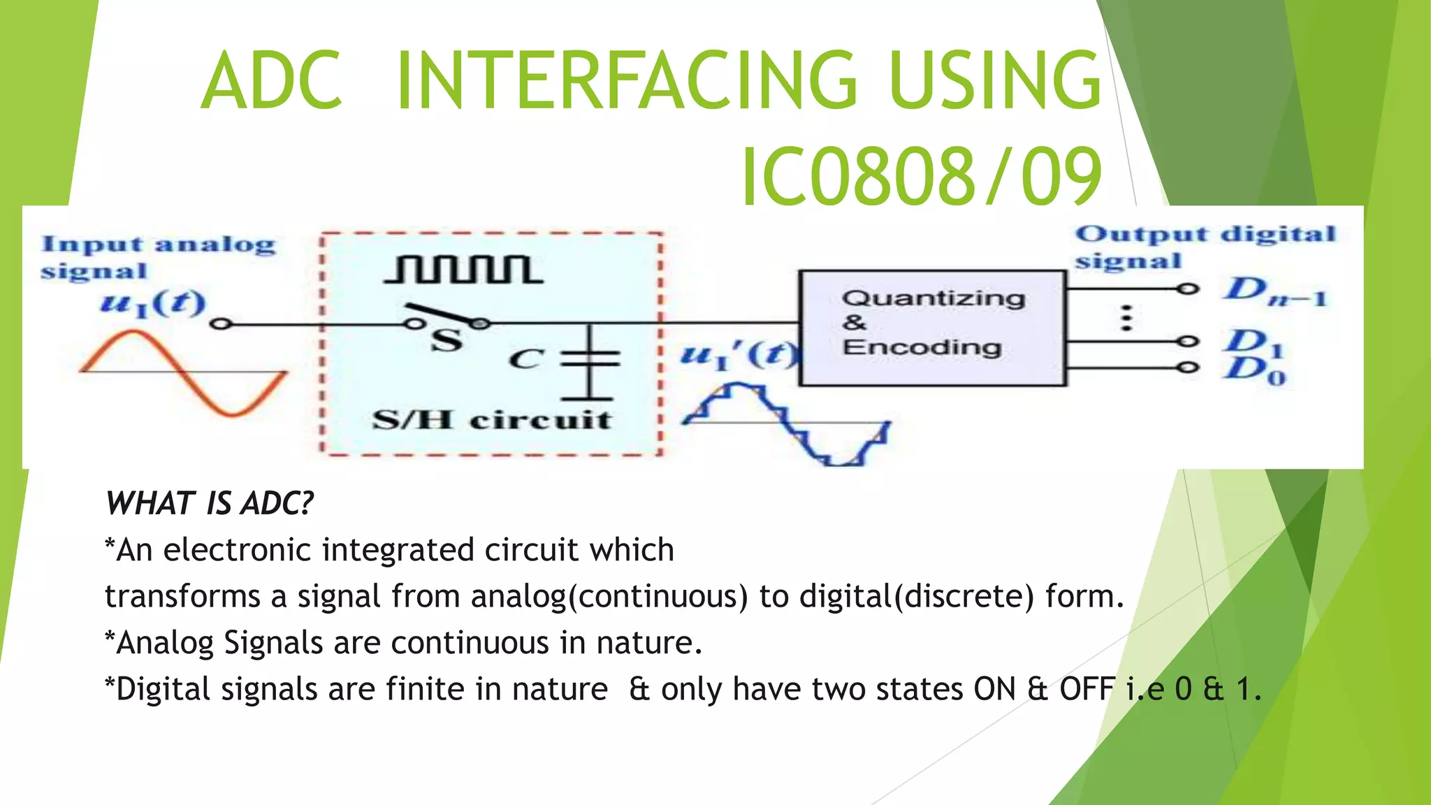
WHATIS ADC?
*An electronic integrated circuit which
transforms a signal from analog(continuous) to digital(discrete) form.
*Analog Signals are continuous in nature.
*Digital signals are finite in nature & only have two states ON & OFF i.e 0 & 1.
3.
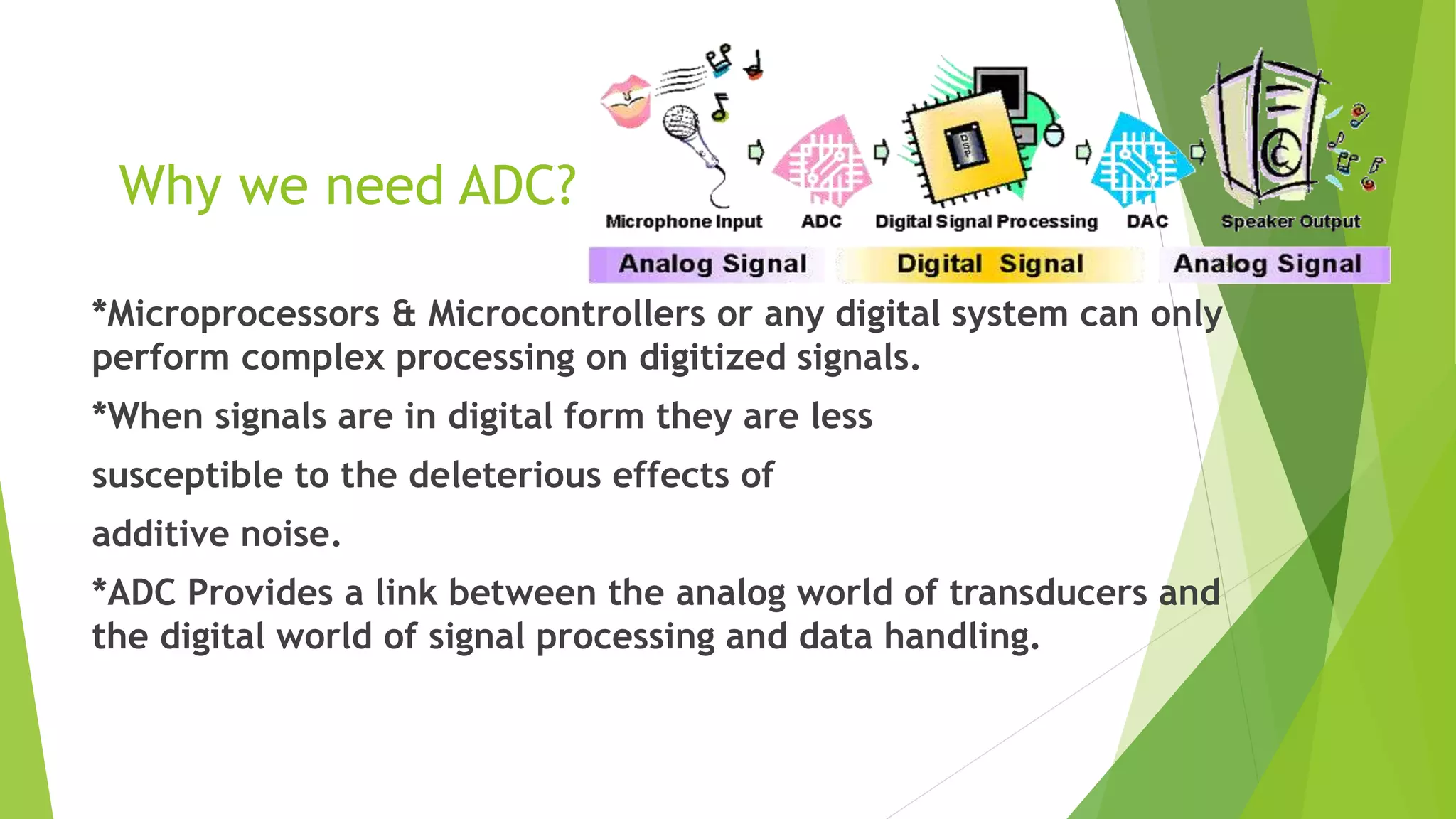
Why we needADC?
*Microprocessors & Microcontrollers or any digital system can only
perform complex processing on digitized signals.
*When signals are in digital form they are less
susceptible to the deleterious effects of
additive noise.
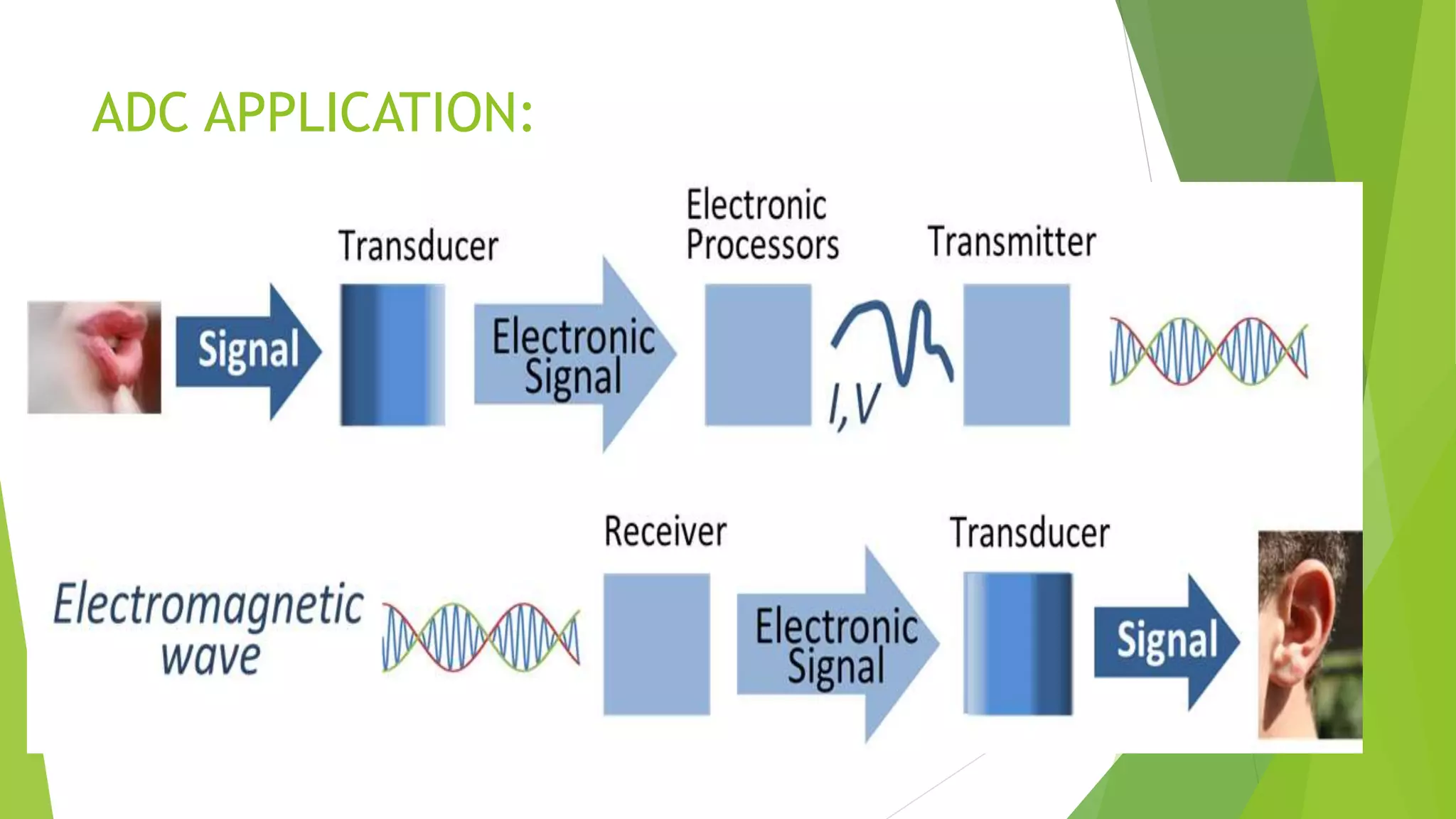
*ADC Provides a link between the analog world of transducers and
the digital world of signal processing and data handling.
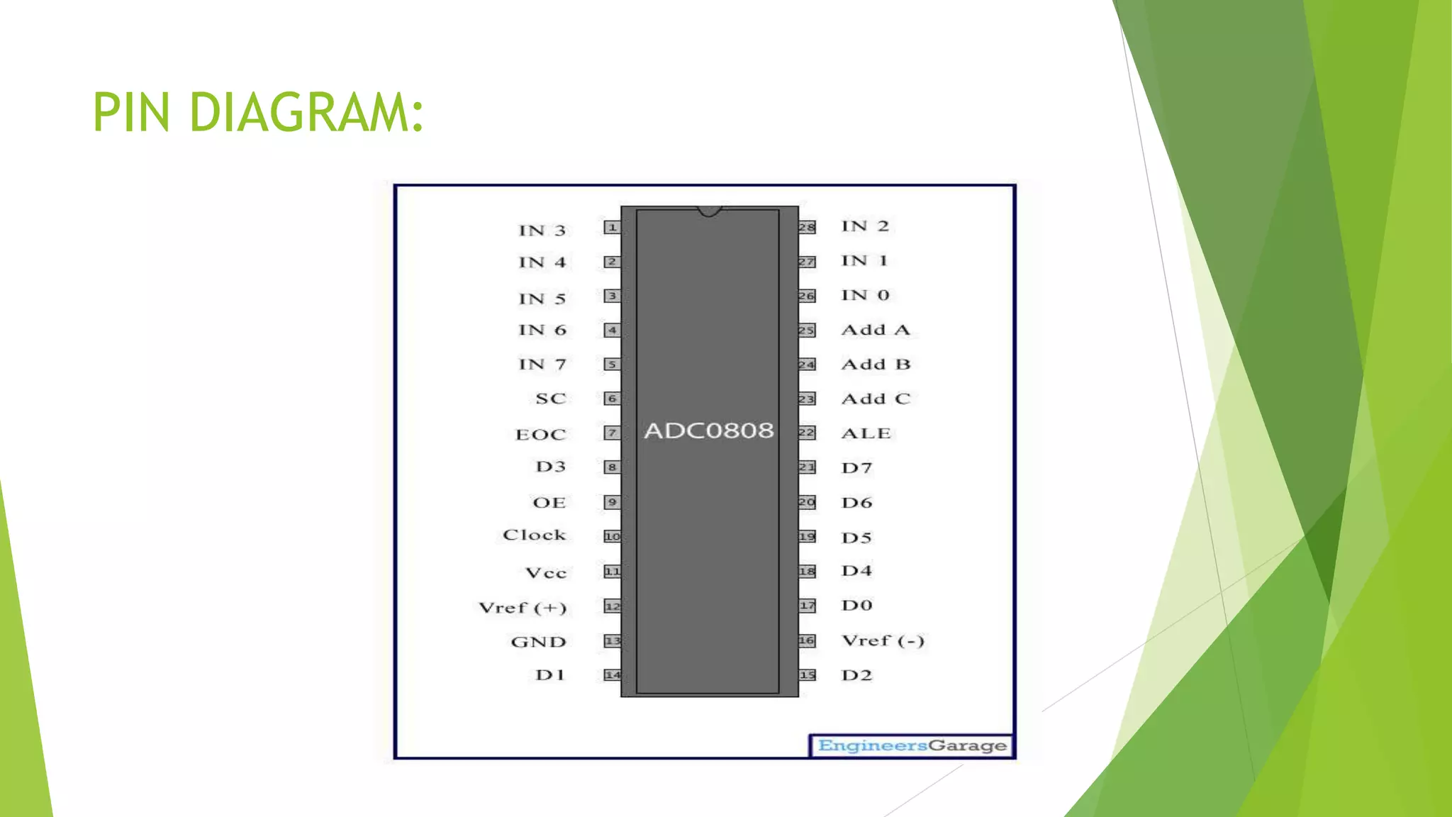
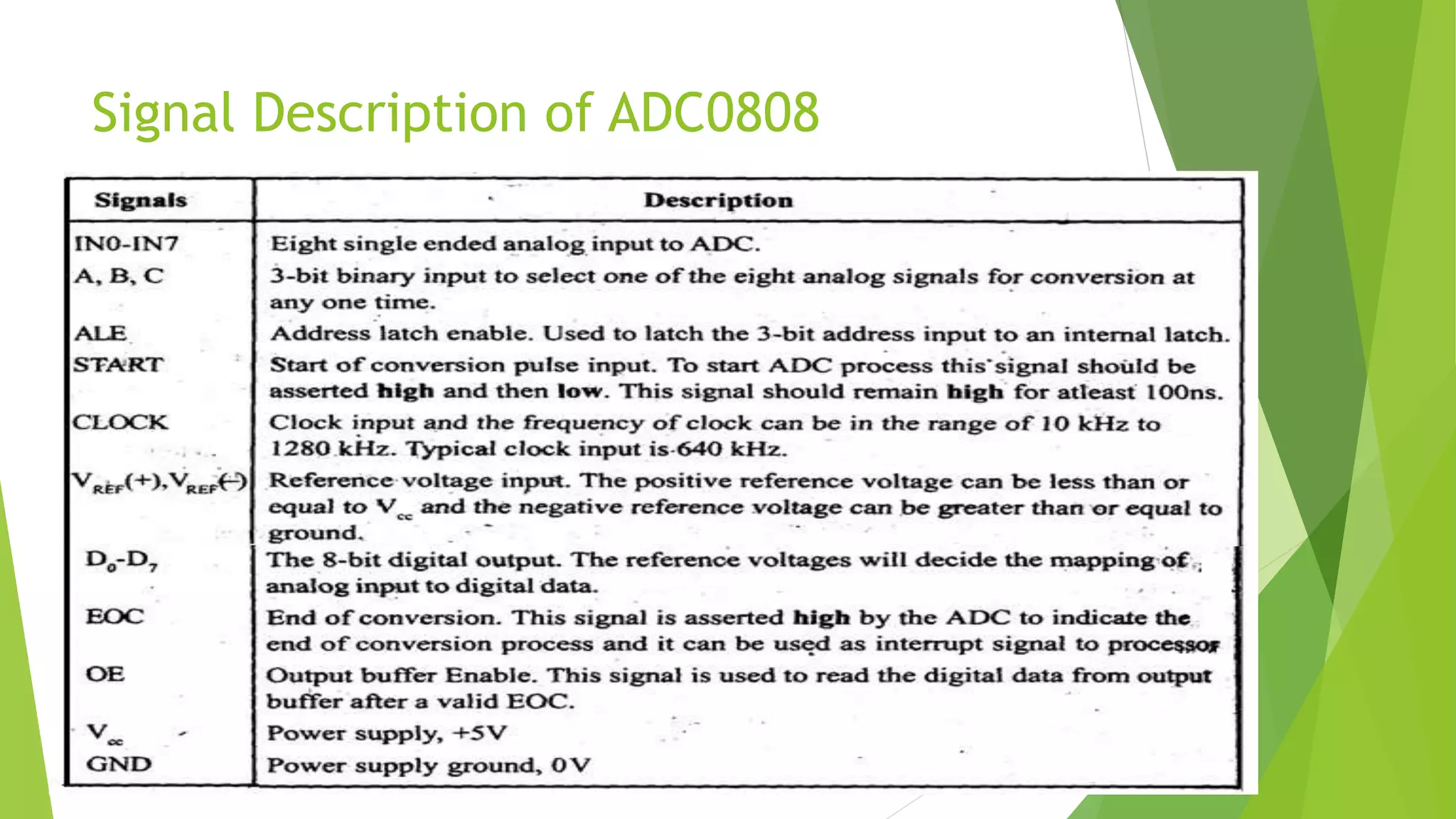
FEATURES OF 0808/0809
28 PIN DIP
Resolution-8 bits
8 INPUT & OUTPUT CHANNELS
Sample Rate (max) (SPS)-10K SPS
Successive approximation technique is used in this IC
High accuracy
High conversion speed[100ms at 640kHz]
8-channel multiplexer with latched control logic
Clock Frequency 10kHz to 1280kHz used clock frequency is 640 KHz
Latched Tri-state output
The IC internally consists of COMPAROTOR SAR, DAC etc.
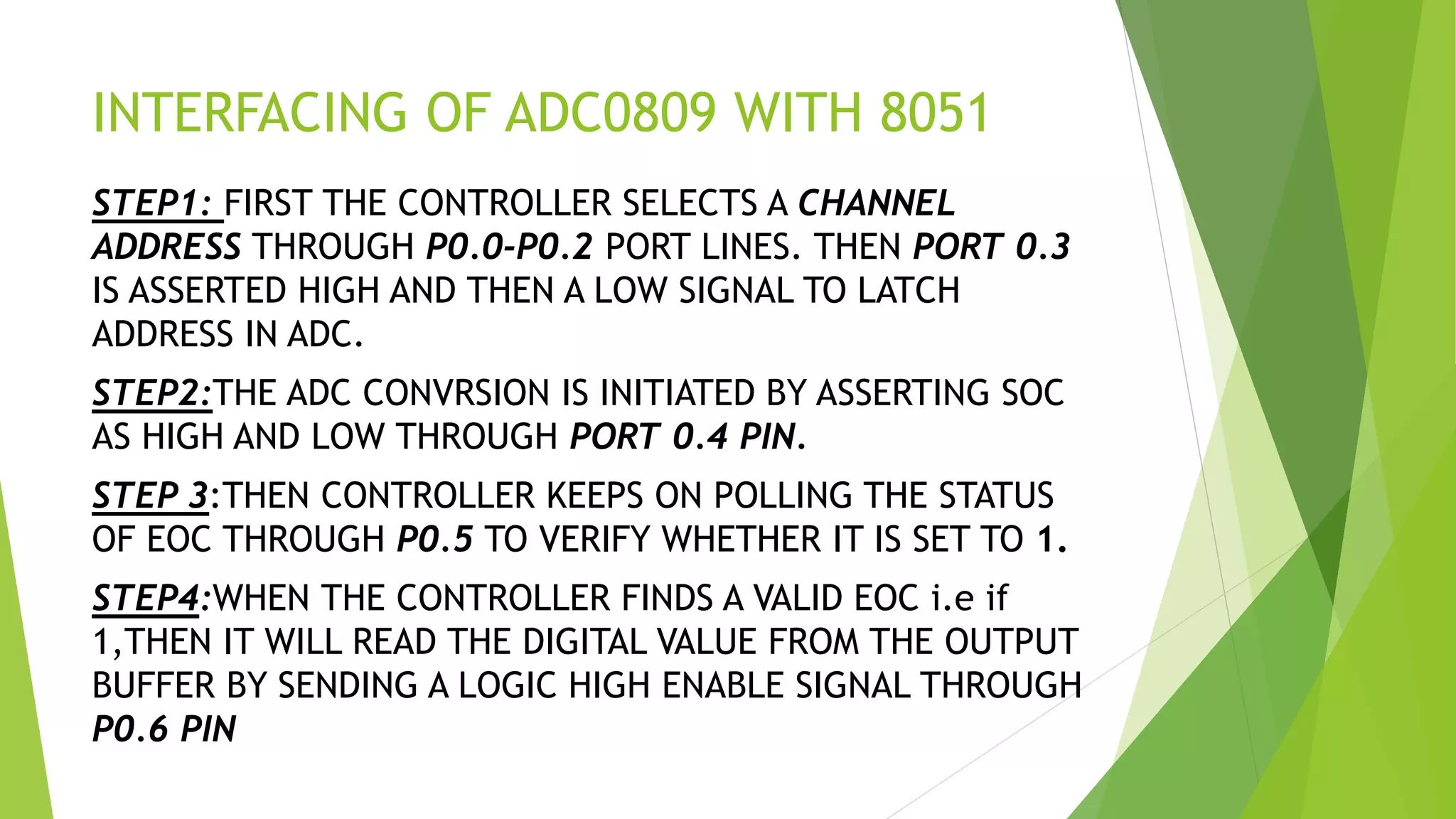
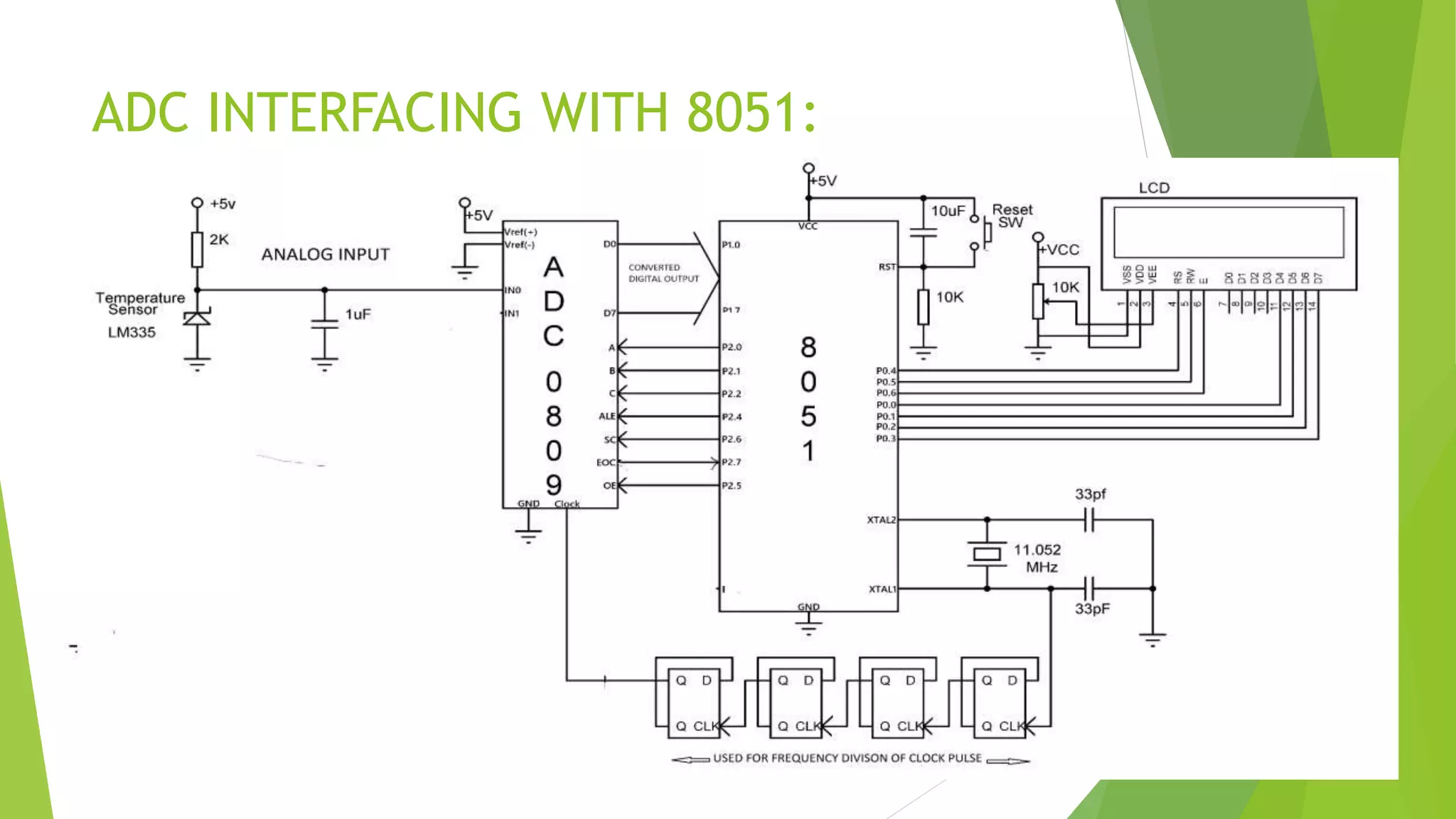
INTERFACING OF ADC0809WITH 8051
STEP1: FIRST THE CONTROLLER SELECTS A CHANNEL
ADDRESS THROUGH P0.0-P0.2 PORT LINES. THEN PORT 0.3
IS ASSERTED HIGH AND THEN A LOW SIGNAL TO LATCH
ADDRESS IN ADC.
STEP2:THE ADC CONVRSION IS INITIATED BY ASSERTING SOC
AS HIGH AND LOW THROUGH PORT 0.4 PIN.
STEP 3:THEN CONTROLLER KEEPS ON POLLING THE STATUS
OF EOC THROUGH P0.5 TO VERIFY WHETHER IT IS SET TO 1.
STEP4:WHEN THE CONTROLLER FINDS A VALID EOC i.e if
1,THEN IT WILL READ THE DIGITAL VALUE FROM THE OUTPUT
BUFFER BY SENDING A LOGIC HIGH ENABLE SIGNAL THROUGH
P0.6 PIN
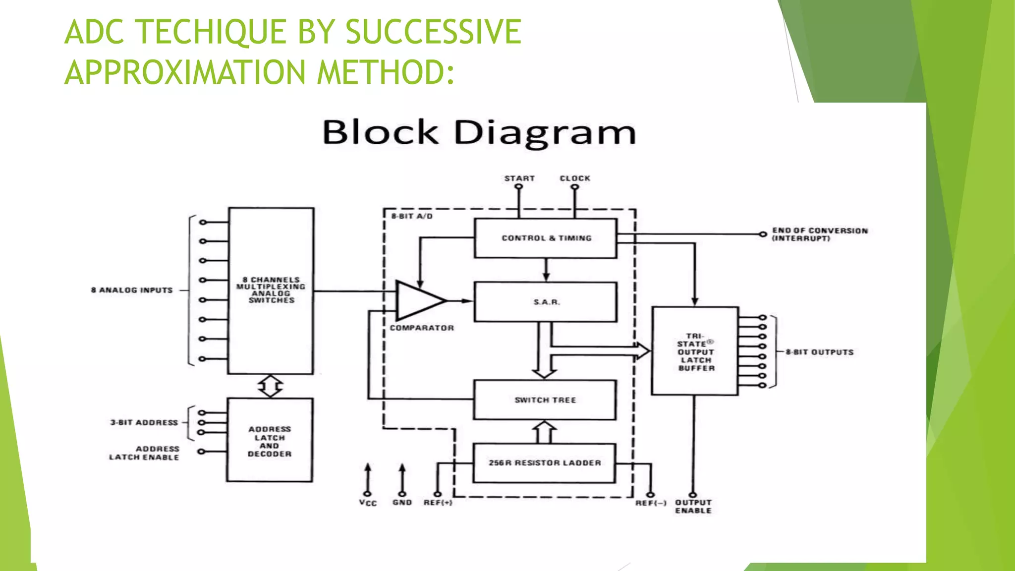
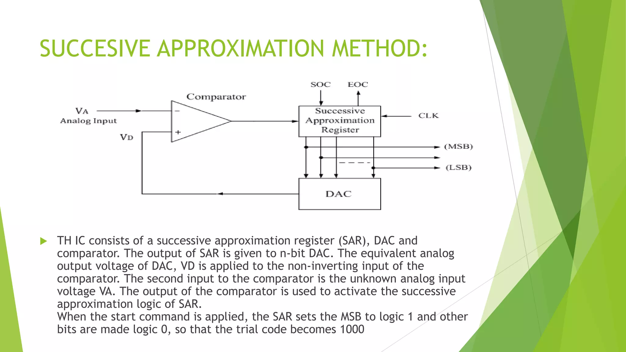
SUCCESIVE APPROXIMATION METHOD:
TH IC consists of a successive approximation register (SAR), DAC and
comparator. The output of SAR is given to n-bit DAC. The equivalent analog
output voltage of DAC, VD is applied to the non-inverting input of the
comparator. The second input to the comparator is the unknown analog input
voltage VA. The output of the comparator is used to activate the successive
approximation logic of SAR.
When the start command is applied, the SAR sets the MSB to logic 1 and other
bits are made logic 0, so that the trial code becomes 1000
11.
SUCCESSIVE APPROXIMATION WORKING:
PLEASE REFER THIS LINK FOR VIDEO ON SUCCESSIVE APPROXIATION
CALCULATION https://www.youtube.com/watch?v=jtb0XXnaYk8
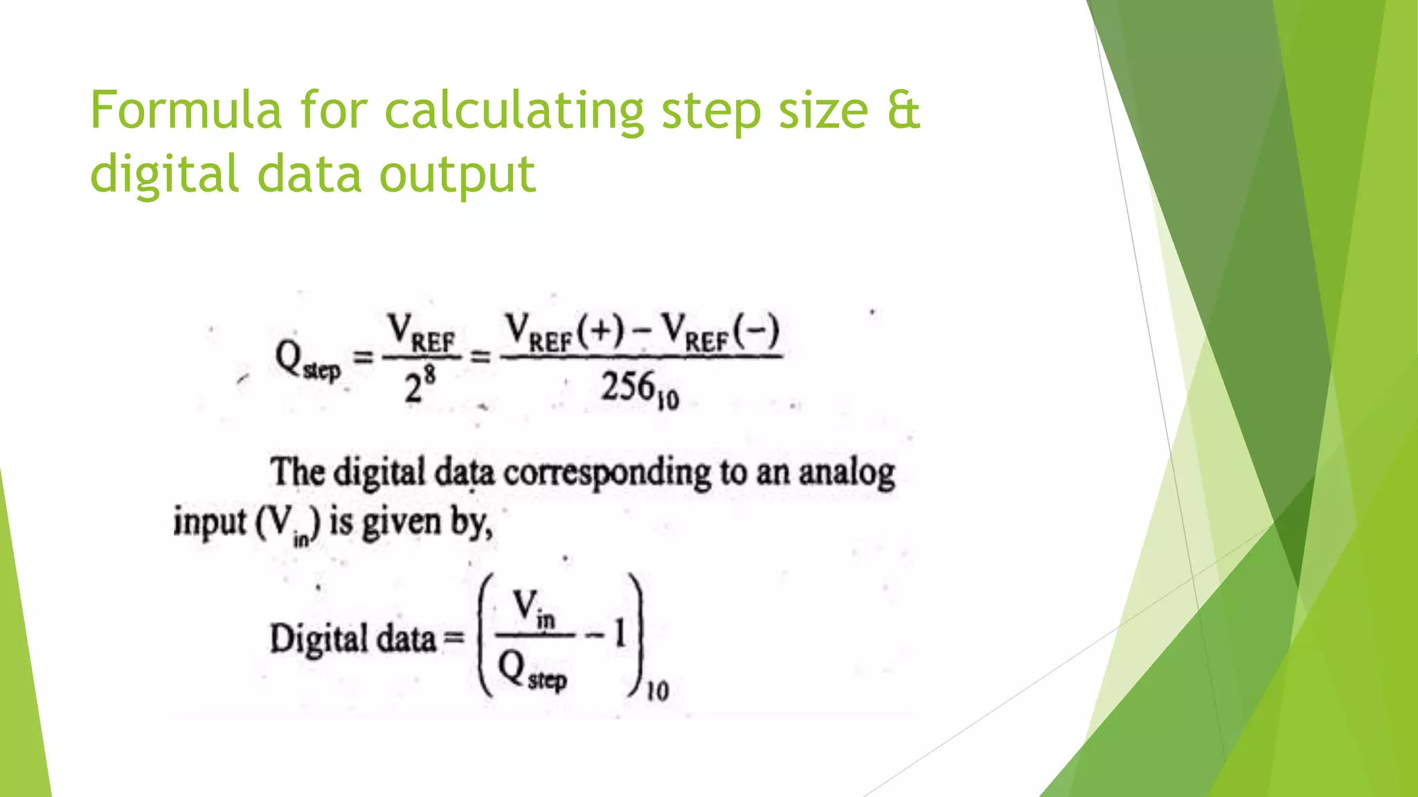
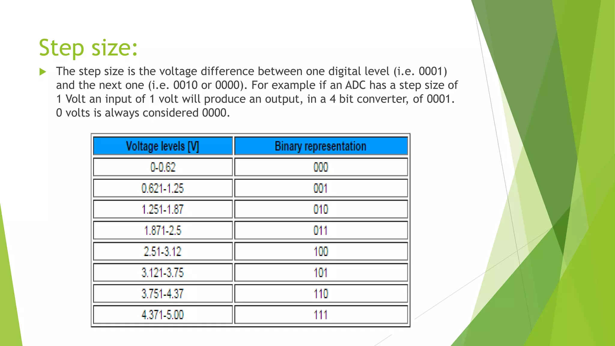
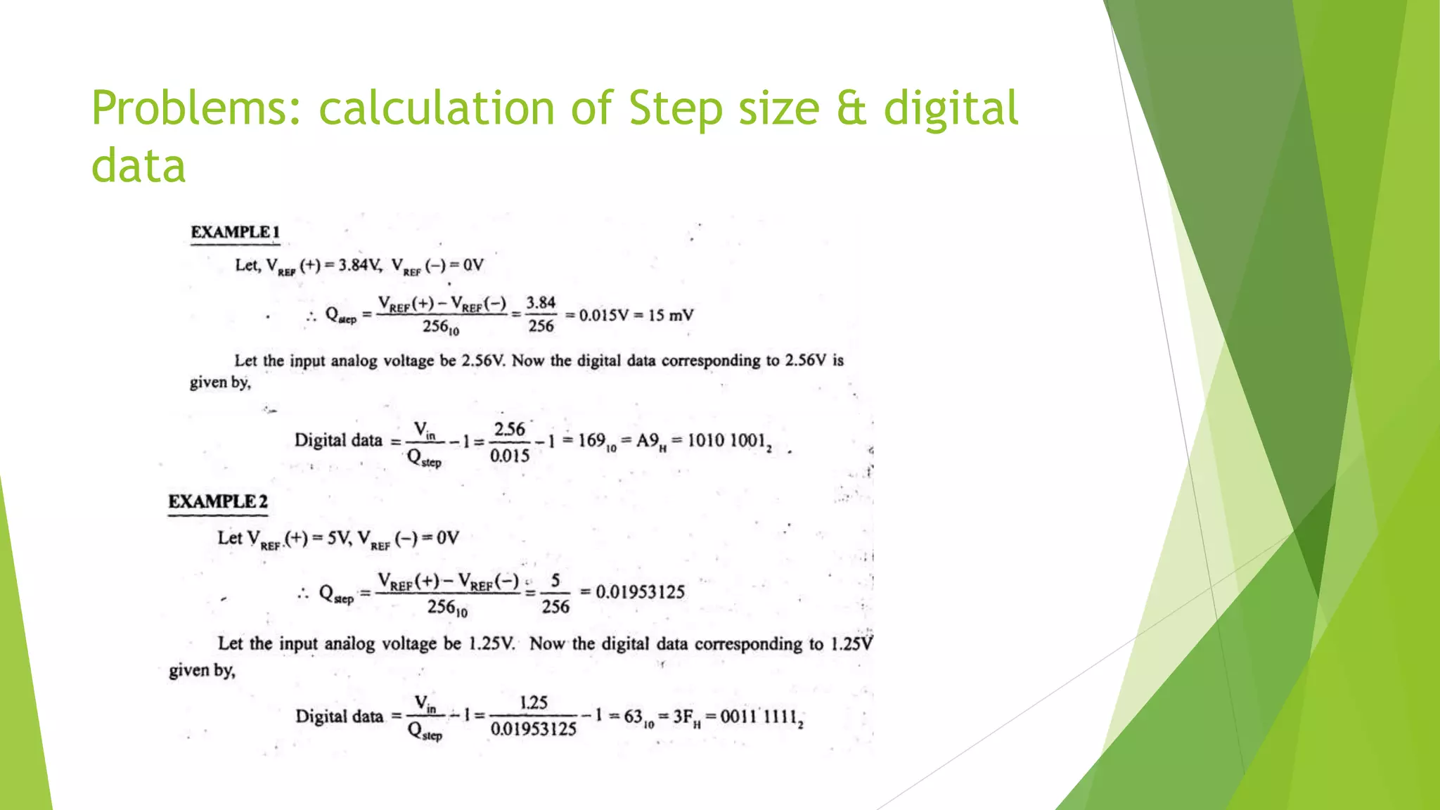
Step size:
Thestep size is the voltage difference between one digital level (i.e. 0001)
and the next one (i.e. 0010 or 0000). For example if an ADC has a step size of
1 Volt an input of 1 volt will produce an output, in a 4 bit converter, of 0001.
0 volts is always considered 0000.
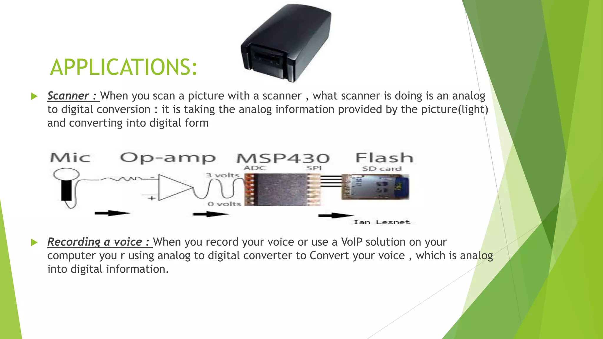
APPLICATIONS:
Scanner :When you scan a picture with a scanner , what scanner is doing is an analog
to digital conversion : it is taking the analog information provided by the picture(light)
and converting into digital form
Recording a voice : When you record your voice or use a VoIP solution on your
computer you r using analog to digital converter to Convert your voice , which is analog
into digital information.
![FEATURES OF 0808/0809
28 PIN DIP
Resolution-8 bits
8 INPUT & OUTPUT CHANNELS
Sample Rate (max) (SPS)-10K SPS
Successive approximation technique is used in this IC
High accuracy
High conversion speed[100ms at 640kHz]
8-channel multiplexer with latched control logic
Clock Frequency 10kHz to 1280kHz used clock frequency is 640 KHz
Latched Tri-state output
The IC internally consists of COMPAROTOR SAR, DAC etc.](https://image.slidesharecdn.com/adc-171021130011/75/INTERFACING-ANALAOG-TO-DIGITAL-CONVERTER-ADC0808-09-TO-8051-MICROCONTROLLER-5-2048.jpg)


![Interfacing technique with 8085- ADC[0808]](https://cdn.slidesharecdn.com/ss_thumbnails/adc-160307140900-thumbnail.jpg?width=640&height=640&fit=bounds)


