Download as PDF, PPTX

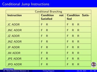
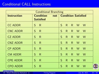
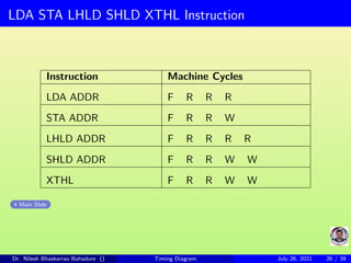
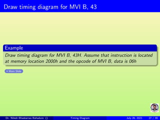
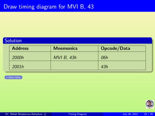
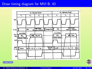
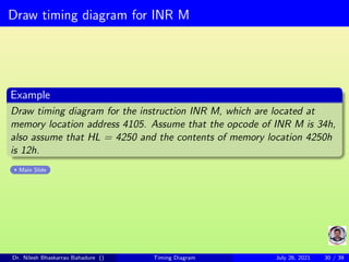
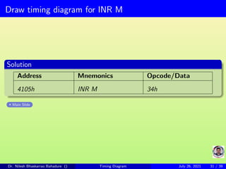
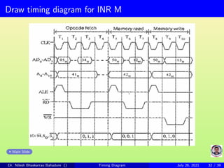
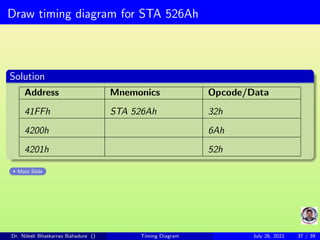
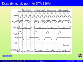


The document provides a detailed overview of the timing diagram for the 8085 microprocessor, outlining various machine cycles, instruction groupings, and their respective execution times represented in t-states. It includes explanations of instruction cycles, machine cycles, and provides examples of specific instructions like conditional jumps and data transfer instructions. Additionally, the author illustrates how to draw timing diagrams for various 8085 instructions with practical examples.