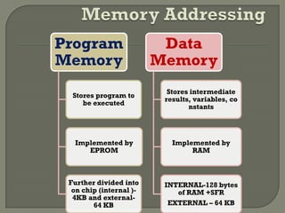
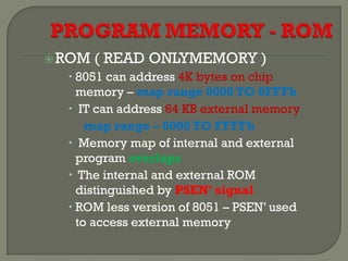
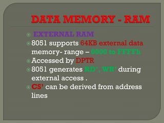
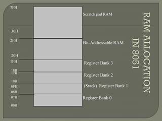
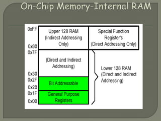
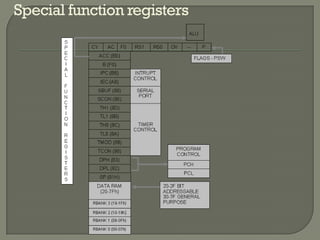
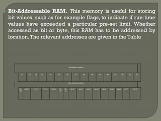
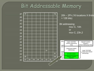
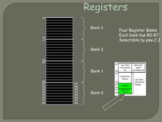
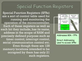
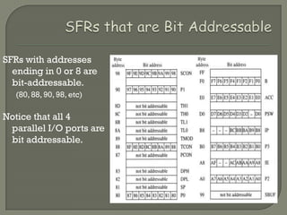
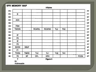
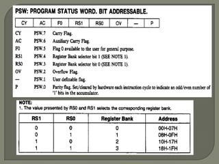
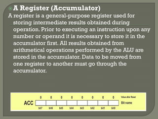
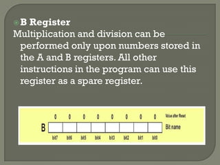
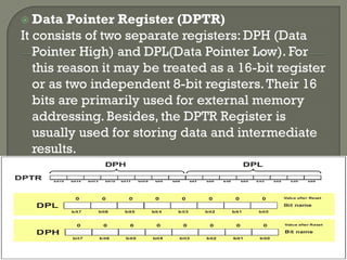
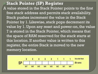
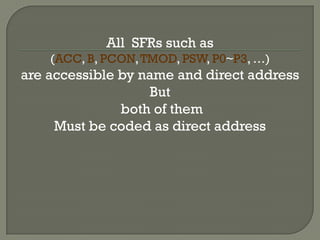
By: Mayank Garg
Program
Memory
Stores program to
be executed
Implemented by
EPROM
Further divided into
on chip (internal )-
4KB and external-
64 KB
Data
Memory
Stores intermediate
results, variables, co
nstants
Implemented by
RAM
INTERNAL-128 bytes
of RAM +SFR
EXTERNAL – 64 KB
ROM ( READ ONLYMEMORY )
 8051 can address 4K bytes on chip
memory – map range 0000 TO 0FFFh
 IT can address 64 KB external memory
map range – 0000 TO FFFFh
 Memory map of internal and external
program overlaps
 The internal and external ROM
distinguished by PSEN’ signal
 ROM less version of 8051 – PSEN’ used
to access external memory
 EXTERNAL RAM
8051 supports 64KB external data
memory- range – 0000 to FFFFh
Accessed by DPTR
8051 generates RD’,WR’ during
external access .
CS’ can be derived from address
lines
7FH
30H
2FH
20H
1FH
17H
10H
0FH
07H
08H
18H
00H
Register Bank 0
(Stack) Register Bank 1
Register Bank 2
Register Bank 3
Bit-Addressable RAM
Scratch pad RAM
8051 CPU Registers
A (Accumulator)
B
PSW (Program Status Word)
SP (Stack Pointer)
PC (Program Counter)
DPTR (Data Pointer)
Used in assembler
instructions
Special function registers
 Bit-Addressable RAM. This memory is useful for storing
bit values, such as for example flags, to indicate if run-time
values have exceeded a particular pre-set limit. Whether
accessed as bit or byte, this RAM has to be addressed by
location.The relevant addresses are given in the Table
Bit Address locations
20 21 22 23 24 25 26 27 28 29 2A 2B 2C 2D 2E 2F
Byte address locations
00-
07
08-0F 10-17 18-1F 20-27 28-
2F
30-
37
38-3F 40-47 48-4F 50-57 58-5F 60-67 68-6F 70-77 78-7F
20h – 2Fh (16 locations X 8-bits
= 128 bits)
7F 78
1A
10
0F 08
07 06 05 04 03 02 01 00
27
26
25
24
23
22
21
20
2F
2E
2D
2C
2B
2A
29
28
Bit addressing:
mov C, 1Ah
or
mov C, 23h.2
Registers
07
06
05
04
03
02
01
00
R7
R6
R5
R4
R3
R2
R1
R0
0F
08
17
10
1F
18
Bank 3
Bank 2
Bank 1
Bank 0
Four Register Banks
Each bank has R0-R7
Selectable by psw.2,3
Special Function Registers (SFRs)
are a sort of control table used for
running and monitoring the
operation of the microcontroller.
Each of these registers as well as
each bit they include, has its name,
address in the scope of RAM and
precisely defined purpose such as
timer control, interrupt control,
serial communication control etc.
Even though there are 128
memory locations intended to be
occupied by them has only 21
such registers.
Addresses 80h – FFh
Direct Addressing
used to access SPRs
SFRs with addresses
ending in 0 or 8 are
bit-addressable.
(80, 88, 90, 98, etc)
Notice that all 4
parallel I/O ports are
bit addressable.
A Register (Accumulator)
A register is a general-purpose register used for
storing intermediate results obtained during
operation. Prior to executing an instruction upon any
number or operand it is necessary to store it in the
accumulator first. All results obtained from
arithmetical operations performed by the ALU are
stored in the accumulator. Data to be moved from
one register to another must go through the
accumulator.
B Register
Multiplication and division can be
performed only upon numbers stored in
the A and B registers. All other
instructions in the program can use this
register as a spare register.
 Data Pointer Register (DPTR)
It consists of two separate registers: DPH (Data
Pointer High) and DPL(Data Pointer Low). For
this reason it may be treated as a 16-bit register
or as two independent 8-bit registers.Their 16
bits are primarily used for external memory
addressing. Besides, the DPTR Register is
usually used for storing data and intermediate
results.
Stack Pointer (SP) Register
A value stored in the Stack Pointer points to the first
free stack address and permits stack availability.
Stack pushes increment the value in the Stack
Pointer by 1. Likewise, stack pops decrement its
value by 1. Upon any reset and power-on, the value
7 is stored in the Stack Pointer, which means that
the space of RAM reserved for the stack starts at
this location. If another value is written to this
register, the entire Stack is moved to the new
memory location.
All SFRs such as
(ACC, B, PCON,TMOD, PSW, P0~P3, …)
are accessible by name and direct address
But
both of them
Must be coded as direct address

8051 memory

  • 1.
  • 2.
    Program Memory Stores program to beexecuted Implemented by EPROM Further divided into on chip (internal )- 4KB and external- 64 KB Data Memory Stores intermediate results, variables, co nstants Implemented by RAM INTERNAL-128 bytes of RAM +SFR EXTERNAL – 64 KB
  • 3.
    ROM ( READONLYMEMORY )  8051 can address 4K bytes on chip memory – map range 0000 TO 0FFFh  IT can address 64 KB external memory map range – 0000 TO FFFFh  Memory map of internal and external program overlaps  The internal and external ROM distinguished by PSEN’ signal  ROM less version of 8051 – PSEN’ used to access external memory
  • 4.
     EXTERNAL RAM 8051supports 64KB external data memory- range – 0000 to FFFFh Accessed by DPTR 8051 generates RD’,WR’ during external access . CS’ can be derived from address lines
  • 5.
    7FH 30H 2FH 20H 1FH 17H 10H 0FH 07H 08H 18H 00H Register Bank 0 (Stack)Register Bank 1 Register Bank 2 Register Bank 3 Bit-Addressable RAM Scratch pad RAM
  • 6.
    8051 CPU Registers A(Accumulator) B PSW (Program Status Word) SP (Stack Pointer) PC (Program Counter) DPTR (Data Pointer) Used in assembler instructions
  • 8.
  • 9.
     Bit-Addressable RAM.This memory is useful for storing bit values, such as for example flags, to indicate if run-time values have exceeded a particular pre-set limit. Whether accessed as bit or byte, this RAM has to be addressed by location.The relevant addresses are given in the Table Bit Address locations 20 21 22 23 24 25 26 27 28 29 2A 2B 2C 2D 2E 2F Byte address locations 00- 07 08-0F 10-17 18-1F 20-27 28- 2F 30- 37 38-3F 40-47 48-4F 50-57 58-5F 60-67 68-6F 70-77 78-7F
  • 10.
    20h – 2Fh(16 locations X 8-bits = 128 bits) 7F 78 1A 10 0F 08 07 06 05 04 03 02 01 00 27 26 25 24 23 22 21 20 2F 2E 2D 2C 2B 2A 29 28 Bit addressing: mov C, 1Ah or mov C, 23h.2
  • 11.
    Registers 07 06 05 04 03 02 01 00 R7 R6 R5 R4 R3 R2 R1 R0 0F 08 17 10 1F 18 Bank 3 Bank 2 Bank1 Bank 0 Four Register Banks Each bank has R0-R7 Selectable by psw.2,3
  • 12.
    Special Function Registers(SFRs) are a sort of control table used for running and monitoring the operation of the microcontroller. Each of these registers as well as each bit they include, has its name, address in the scope of RAM and precisely defined purpose such as timer control, interrupt control, serial communication control etc. Even though there are 128 memory locations intended to be occupied by them has only 21 such registers. Addresses 80h – FFh Direct Addressing used to access SPRs
  • 13.
    SFRs with addresses endingin 0 or 8 are bit-addressable. (80, 88, 90, 98, etc) Notice that all 4 parallel I/O ports are bit addressable.
  • 16.
    A Register (Accumulator) Aregister is a general-purpose register used for storing intermediate results obtained during operation. Prior to executing an instruction upon any number or operand it is necessary to store it in the accumulator first. All results obtained from arithmetical operations performed by the ALU are stored in the accumulator. Data to be moved from one register to another must go through the accumulator.
  • 17.
    B Register Multiplication anddivision can be performed only upon numbers stored in the A and B registers. All other instructions in the program can use this register as a spare register.
  • 18.
     Data PointerRegister (DPTR) It consists of two separate registers: DPH (Data Pointer High) and DPL(Data Pointer Low). For this reason it may be treated as a 16-bit register or as two independent 8-bit registers.Their 16 bits are primarily used for external memory addressing. Besides, the DPTR Register is usually used for storing data and intermediate results.
  • 19.
    Stack Pointer (SP)Register A value stored in the Stack Pointer points to the first free stack address and permits stack availability. Stack pushes increment the value in the Stack Pointer by 1. Likewise, stack pops decrement its value by 1. Upon any reset and power-on, the value 7 is stored in the Stack Pointer, which means that the space of RAM reserved for the stack starts at this location. If another value is written to this register, the entire Stack is moved to the new memory location.
  • 20.
    All SFRs suchas (ACC, B, PCON,TMOD, PSW, P0~P3, …) are accessible by name and direct address But both of them Must be coded as direct address