Download to read offline
![Srijan Chatterjee, V.V.Subrahmanya Kumar Bhajana / International Journal of Engineering
Research and Applications (IJERA) ISSN: 2248-9622 www.ijera.com
Vol. 3, Issue 3, May-Jun 2013, pp.543-547
546 | P a g e
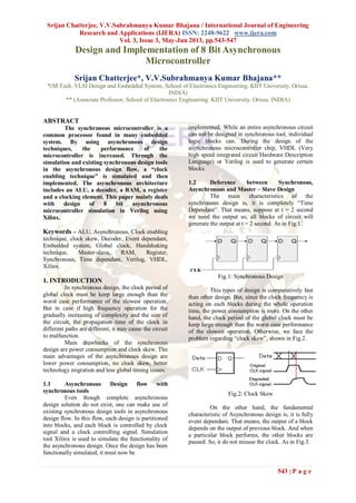
Fig.13: Simulated result of COMP between 2 and 1
This is the simulation result of comparison between
2 and 1. If first input „a‟ is larger than second input
„b‟ then the output will be 1, otherwise 0.
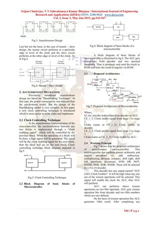
Fig.14: Simulated result of Right Shift (4 shifted by
2bit)
Fig.15: Simulated result of AND operation (1 AND
1)
Fig.16: Simulated result of OR operation (4 OR 1)
4. CONCLUSION
This paper is mainly deals with the
simulation and its implementation of the
asynchronous design of an 8bit microcontroller
with clock controlling technique. Using which
technique in a circuit block we can make activated
the working block only and the other blocks are
paused.
The above technique is very much useful in low
power applications viz. Bio medical instruments,
mobile phones etc.
5. ACKNOWLEDGEMENT
First of all I would like to thank my guide
B.V.V.Subrahmanya Kumar for guiding me
throughout the research part of the thesis. I am
really privileged to have opportunity to work with
him.
I will also thank Prof. S.K.Mandal
(Associate Dean, School of Electronics
Engineering, KIIT University, Bhubaneswar,
Orissa) for supporting me throughout my research
work. I am also thankful to Assistant Professor Mr.
Ankit Shivare for all his guidance and pleasant
work everyday in the lab. I am also thankful to all
the staffs and employees of School of Electronics
Engineering of KIIT University.
I am really also grateful to my friends
Pratik Ganguly and Abhinab Anand for all their
helping hands during my days of research.
Finally, last but not the least I pay all my sincere
gratitude towards my loving mother and caring
father for supporting throughout my sorrow and
best days of my life.
REFERENCES
[1] Raj Kamal, Embedded systems (The
McGraw Hill Companies)
[2] Muhammad Ali Mzidi, Janice Gillispie
Mazidi, The 8051 microcontroller and
embedded sysytems
[3] Peter Marwedel, Embedded system design
(Springer)](https://image.slidesharecdn.com/cn33543547-130523023141-phpapp01/85/Cn33543547-4-320.jpg)
![Srijan Chatterjee, V.V.Subrahmanya Kumar Bhajana / International Journal of Engineering
Research and Applications (IJERA) ISSN: 2248-9622 www.ijera.com
Vol. 3, Issue 3, May-Jun 2013, pp.543-547
547 | P a g e
[4] Kok – Leong Chang, Bah – Hwee Gwee,
Centre for Integrated Circuits and
Systems, Nayang Technological
University, Singapore, A low – energy low
– voltage asynchronous 8051
microcontroller core, 2006 IEEE.
[5] Hans van Gageldonk, Eindhoven
University of Technology, The
Netherlands, Kees van Berkel, Ad Peeters,
Philips Research Laboratories, The
Netherlands, Daniel Baumann, Daniel
Gloor, Gerhard Stegmann, Philips
Semiconductors, Zurich, Switzerland, An
asynchronous low – power 80C51
microcontroller.
[6] Kok – Leong Chang and Bah – Hwee
Gwee, Centre for Integrated Circuits and
Systems, Nayang Technological
University, Singapore, Yuanjin Zheng,
Integrated Circuits and Systems
Laboratory, Institute of Microelectronics,
Singapore, A semi – custom memory
design for an asynchronous 8051
microcontroller, 2008 IEEE.
[7] YU Ying, ZHOU Lei, MIN Hao, ASIC &
System State – Key Lab, Fudan
University, Shanghai, China, Design and
vlsi implementation of an asynchronous
low power microcontroller.
[8] Jamin M.C.Tse and Daniel P.K.Lun,
Department of Electronics Engineering,
The Hong Kong polytechnique University,
Hong Kong, Asynmpu: a fully
asynchronous cics micro – processor,
1997 IEEE International Symposium on
Circuits and Systems, June 9 – 12, 1997.
[9] Hans Jacobson, Department of Computer
Engineering, Lulea University of
Technology, Asynchronous circuit design,
May 1996.](https://image.slidesharecdn.com/cn33543547-130523023141-phpapp01/85/Cn33543547-5-320.jpg)

This paper discusses the design and implementation of an 8-bit asynchronous microcontroller, emphasizing its advantages over synchronous microcontrollers such as lower power consumption and the absence of clock skew. A new clock controlling technique is proposed to manage operations across different blocks using a clock enabling signal, facilitating efficient functioning in low power applications. The design was simulated using Xilinx and is illustrated with various operational results, showcasing the functionality of the microcontroller in performing multiple arithmetic and logical operations.