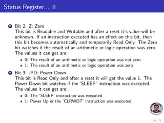
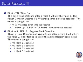
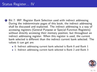
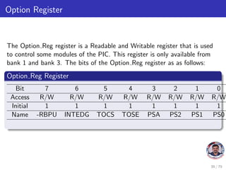
Download as PDF, PPTX

![References
[1, 2, 3, 4]
Muhammad Ali Mazidi, Rolin D. McKinlay, and Danny Causey.
PIC Microcontroller and Embedded Systems - Using Assembly and C
for PIC18.
Pearson International Edition, Upper Saddle River, NJ, 2008.
Martin P. Bates.
Programming 8 - bit PIC Microcontrollers in C with Interactive
Hardware Simulation.
Newnes Press Private Limited, United Kingdom, 2008.
Ajay V. Deshmukh.
Microcontrollers Theory and Applications.
Tata McGraw Hill, New Delhi, India, 2008.
John B. Peatman.
Design with PIC Microcontroller.
Prentice Hall, New Delhi, India, 1997.
78 / 79](https://image.slidesharecdn.com/microcontrollerpic16f877registersmemoryports-210701072829/85/Microcontroller-pic-16-f877-registers-memory-ports-78-320.jpg)


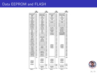
The document provides a comprehensive overview of the PIC16F877 microcontroller, detailing its architecture, registers, I/O ports, memory organization, and programming techniques. It outlines the course objectives, including understanding its features, learning assembly and C programming, and performing hardware interfacing. Additionally, it covers special function registers, data memory organization, and the functionalities of various I/O ports.