8051 Architecture and PIN Configuration.pdf
•
0 likes•835 views

The document discusses the 8051 microcontroller. It begins by describing the key features of the 8051 microcontroller, including that it has an 8-bit CPU, 4KB of internal program memory, 128 bytes of internal data memory, 32 I/O lines that can be used as ports, and two 16-bit timer counters. It then provides more details on the internal architecture, describing the ALU, registers, memory organization, and other components. It concludes by explaining features like the register banks and stack memory.
![Microcontrollers T.Srikrishna, M.Sc , M.Tech, GVP
Embedded Systems Examples
Salient features of 8051 microcontroller
8051 Microcontroller is designed by Intel in 1981.
A Microcontroller is a programmable digital processor with necessary peripherals.
Eight bit CPU
On chip clock oscillator
4Kbytes of internal program memory (code memory) [ROM]
128 bytes of internal data memory [RAM]
64 Kbytes of external program memory address space.
64 Kbytes of external data memory address space.
32 bi directional I/O lines (can be used as four 8 bit ports or 32 individually
addressable I/O lines)
Two 16 Bit Timer/Counter :T0, T1
Full Duplex serial data receiver/transmitter
Four Register banks with 8 registers in each bank.
Sixteen bit Program counter (PC) and a data pointer (DPTR)
8 Bit Program Status Word (PSW)
8 Bit Stack Pointer
Five vector interrupt structure (RESET not considered as an interrupt.)](data:image/gif;base64,R0lGODlhAQABAIAAAAAAAP///yH5BAEAAAAALAAAAAABAAEAAAIBRAA7)
Recommended
More Related Content
What's hot
What's hot (20)
Similar to 8051 Architecture and PIN Configuration.pdf
Similar to 8051 Architecture and PIN Configuration.pdf (20)
More from Srikrishna Thota
More from Srikrishna Thota (19)
Recently uploaded
Recently uploaded (20)
8051 Architecture and PIN Configuration.pdf
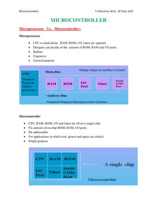
- 1. Microcontrollers T.Srikrishna, M.Sc , M.Tech, GVP MICROCONTROLLER Microprocessor Vs. Microcontroller: Microprocessor CPU is stand-alone, RAM, ROM, I/O, timer are separate Designer can decide on the amount of ROM, RAM and I/O ports. Bulkier Expensive General-purpose Microcontroller CPU, RAM, ROM, I/O and timer are all on a single chip Fix amount of on-chip ROM, RAM, I/O ports Bit addressable For applications in which cost, power and space are critical Single-purpose
- 2. Microcontrollers T.Srikrishna, M.Sc , M.Tech, GVP Embedded Systems Examples Salient features of 8051 microcontroller 8051 Microcontroller is designed by Intel in 1981. A Microcontroller is a programmable digital processor with necessary peripherals. Eight bit CPU On chip clock oscillator 4Kbytes of internal program memory (code memory) [ROM] 128 bytes of internal data memory [RAM] 64 Kbytes of external program memory address space. 64 Kbytes of external data memory address space. 32 bi directional I/O lines (can be used as four 8 bit ports or 32 individually addressable I/O lines) Two 16 Bit Timer/Counter :T0, T1 Full Duplex serial data receiver/transmitter Four Register banks with 8 registers in each bank. Sixteen bit Program counter (PC) and a data pointer (DPTR) 8 Bit Program Status Word (PSW) 8 Bit Stack Pointer Five vector interrupt structure (RESET not considered as an interrupt.)
- 3. Microcontrollers T.Srikrishna, M.Sc , M.Tech, GVP 8051 CPU consists of 8 bit ALU with associated registers like accumulator ‘A’ , B register, ALU can perform arithmetic and logic functions on 8 bit variables. 8051 has 128 bytes of internal RAM which is divided into 1. Working registers [00 – 1F] 2. Bit addressable memory area [20 – 2F] 3. General purpose memory area (Scratch pad memory) [30-7F] Pin Configuration Pins 1 to 8 − These pins are known as Port 1. Each of these pins can be configured as an input or an output means bi-directional I/O port. Pin 9 − It is a RESET pin, which is used to reset the microcontroller to its initial values.
- 4. Microcontrollers T.Srikrishna, M.Sc , M.Tech, GVP Pins 10 to 17 − These pins are known as Port 3. each of these pins can serve as general input or output pins. Besides, all of them have alternative functions o Pin 10 RXD. Serial asynchronous communication input or Serial synchronous communication output. o Pin 11 TXD. Serial asynchronous communication output or Serial synchronous communication clock output. o Pin 12 INT0.External Interrupt 0 input o Pin 13 INT1. External Interrupt 1 input o Pin 14 T0. Counter 0 clock input o Pin 15 T1. Counter 1 clock input o Pin 16 WR. Write to external (additional) RAM o Pin 17 RD. Read from external RAM Pins 18 & 19 − These pins are used for interfacing an external crystal to get the system clock. Pin 20 − This pin provides the power supply to the circuit. Pins 21 to 28 − These pins are known as Port 2. It serves as I/O port. Higher order address bus signals are also multiplexed using this port. Pin 29 − This is PSEN pin which stands for Program Store Enable. It is used to read a signal from the external program memory. Pin 30 − This is EA pin which stands for External Access input. It is used to enable/disable the external memory interfacing. Pin 31 − This is ALE pin which stands for Address Latch Enable. It is used to demultiplex the address-data signal of port. Pins 32 to 39 − These pins are known as Port 0. It serves as I/O port. Lower order address and data bus signals are multiplexed using this port. Pin 40 − This pin is used to provide power supply to the circuit.
- 5. Microcontrollers T.Srikrishna, M.Sc , M.Tech, GVP Block Diagram of 8051 ALU: It is 8 bit unit. It performs arithmetic operation as addition, subtraction, multiplication, division, increment and decrement. It performs logical operations like AND, OR and EX-OR. Accumulator(A-reg): It is 8 bit register. It is used to store 8 bit data and to hold one of operand of ALU units during arithmetical and logical operations. Result of arithmetic & logic operations performed by ALU is accumulated by this register. Therefore it is called accumulator register. B-register: It is bit and byte accessible. It is used in conjunction with A register as I/P operand for ALU. It is used as general purpose register to store 8 bit data. A and B registers together is also called MATH registers Stack Pointer (SP) –It is 8-bit register. It is used to hold the internal RAM memory location addresses which are used as stack memory. Data pointer register (DTPR): It is a 16 bit register used to hold address of external or internal RAM where data is stored or result is to be stored. It is used to store 16 bit data. It is divided into2- 8bit registers. DPH-data pointer higher order (83H) and DPL-data pointer lower order (82H). Each register can be used as general purpose register to store 8 bit data and can also be used as memory location. Program Counter (PC) – 16 bit PC contains the address of next instruction to be executed. On reset PC will set to 0000. After fetching every instruction PC will increment by one.
- 6. Microcontrollers T.Srikrishna, M.Sc , M.Tech, GVP Flag Bits and PSW Register The 8051 has four math flags and three general-purpose user flags ,they are grouped inside the program status word (PSW) and the power control (PCON) registers. The math flags include carry (C), auxiliary carry (AC), overflow (OV), and parity (P). User flags are named FO, GFO, and GF1; they are general-purpose flags that may be used by the programmer to record some event in the program. that can be set to I or cleared to 0 by the programmer as desired Program Status Word : This is an 8 bit register which contains the arithmetic status of ALU and the bank select bits of register banks. Power control register (PCON): it is 8-bit register. Its bits are used to control mode of power saving circuit, either idle or power down mode and also one bit is used to modify baud rate of serial communication
- 7. Microcontrollers T.Srikrishna, M.Sc , M.Tech, GVP Special function Registers(SFR): The 8051 microcontroller has 11 SFR divided in 4 groups: Timer/Counter register: 8051 microcontroller has two-16 bit Timer/counter registers 8051 microcontroller has two 8-bit timer control register i.e. TMOD and TCON register. TMOD Register: it is 8-bit register. It used to select mode and control operation of time by writing control word. TCON register: It is 8-bit register. It is used to control operation of timer/ counter and external interrupt . Serial data register: 8051 micro controller has 2 serial data registers SBUF and SCON. Serial buffer register (SBUF): it is 8-bit register. It is used to hold data which is to be transferred serially. Serial control register (SCON): it is 8-bit register. The 8-bit loaded into this register controls the operation of serial communication. Interrupt register: 8051 µC has two 8-bit interrupt register. Interrupt enable register (IE): it is 8-bit register. it is used to enable and disable function of interrupt. Interrupt priority register (IP): It is 8-bit register. it is used to select low or high level priority of each individual interrupts. Memory Organization 0f 8051 The memory organization of 80851 is classified into two types 1. Data Memory or RAM 2. Program Memory or ROM 1.Data Memory or RAM (a) Internal RAM/Data Memory : • There are 128 bytes of RAM in the 8051. – Assigned addresses 00 to 7FH • The 128 bytes are divided into 3 different groups as follows: – A total of 32 bytes from locations 00 to 1F hex are set aside for register banks and the stack. – A total of 16 bytes from locations 20H to 2FH are set aside for bit-addressable read/write memory. – A total of 80 bytes from locations 30H to 7FH are used for read and write storage, called scratch pad.
- 8. Microcontrollers T.Srikrishna, M.Sc , M.Tech, GVP (b) External RAM /Data Memory: Access to external memory is slower than access to internal data memory. There may be up to 64K Bytes of external data memory.
- 9. Microcontrollers T.Srikrishna, M.Sc , M.Tech, GVP Program Memory or Code Memory EA'(bar) and PSEN' determines whether Internal ROM is accessed or External ROM is accessed. Internal ROM 8051 has 4 KB internal Read Only Memory. It mainly contains some executable functions and some data which may never change. Address range is 0000H to 0FFFH. EA'=1 In this case, the microcontroller executes first the program from built-in ROM, then the program stored in external memory. External ROM EA'=0 In this case, the microcontroller completely ignores internal program memory and executes only the program stored in external memory. Address range is 0000H to FFFFH. Register Banks in 8051 A total of 32 bytes of RAM are set aside for the register banks and the stack. These 32 bytes are divided into four register banks in which each bank has 8 registers, R0–R7..
- 10. Microcontrollers T.Srikrishna, M.Sc , M.Tech, GVP Default Register Bank If RAM locations 00–1F are set aside for the four registers banks, which register bank of R0–R7 do we have access to when the 8051 is powered up? The answer is register bank 0 How to Switch Register Banks D4 and D3 bits of the PSW are used to select the desired register bank, since they can be accessed by the bit addressable instructions SETB and CLR. For example, "SETB PSW.3" will set PSW.3 = 1 and select the bank register 1. Stack in the 8051 The stack is a section of a RAM used by the CPU to store information such as data or memory address on temporary basis. How Stacks are Accessed As the stack is a section of a RAM, the register used to access the stack is known as the stack pointer register. The stack pointer in the 8051 is 8-bits wide. When the 8051 is initialized, the SP register contains the value 07H. This means that the RAM location 08 is the first location used for the stack. The storing operation of a CPU register in the stack is known as a PUSH, and getting the contents from the stack back into a CPU register is called a POP.
- 11. Microcontrollers T.Srikrishna, M.Sc , M.Tech, GVP