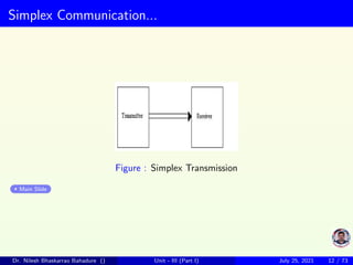
Download as PDF, PPTX


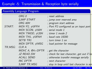
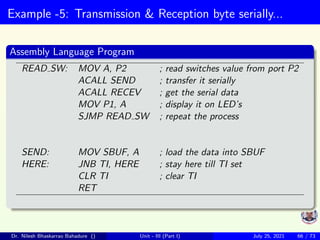
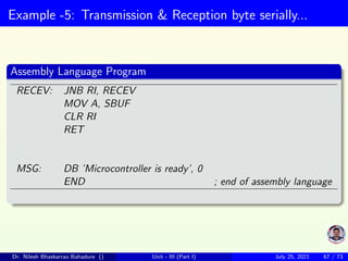
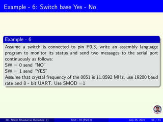


The document provides an overview of serial communication in the 8051 microcontroller, focusing on the Universal Asynchronous Receiver Transmitter (UART) and its modes of operation, including simplex, half duplex, and full duplex communication. It details methods of serial data transmission, programming considerations, the significance of baud rate, and how to configure data transfer rates. Additionally, it discusses the SCON register and the importance of specific flags for managing communication effectively.