Downloaded 276 times


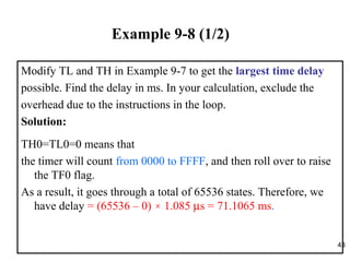


The document discusses timer programming for the 8051 microcontroller. It contains the following information: - The 8051 has two timers/counters that can be used as timers to generate time delays or as event counters. - Timers use 1/12 of the crystal frequency as the input clock. Registers like TH0, TL0, TMOD, and TCON are used to program and control the timers. - Timer Mode 1 is a 16-bit timer mode where the TH and TL registers increment continuously until they roll over, setting the timer flag. Programming involves initializing the registers, starting the timer, and monitoring the flag.