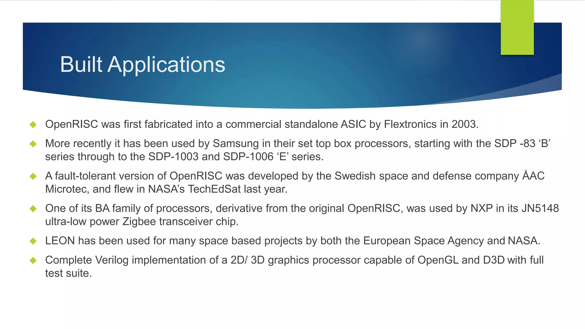
Downloaded 314 times
![VHDL
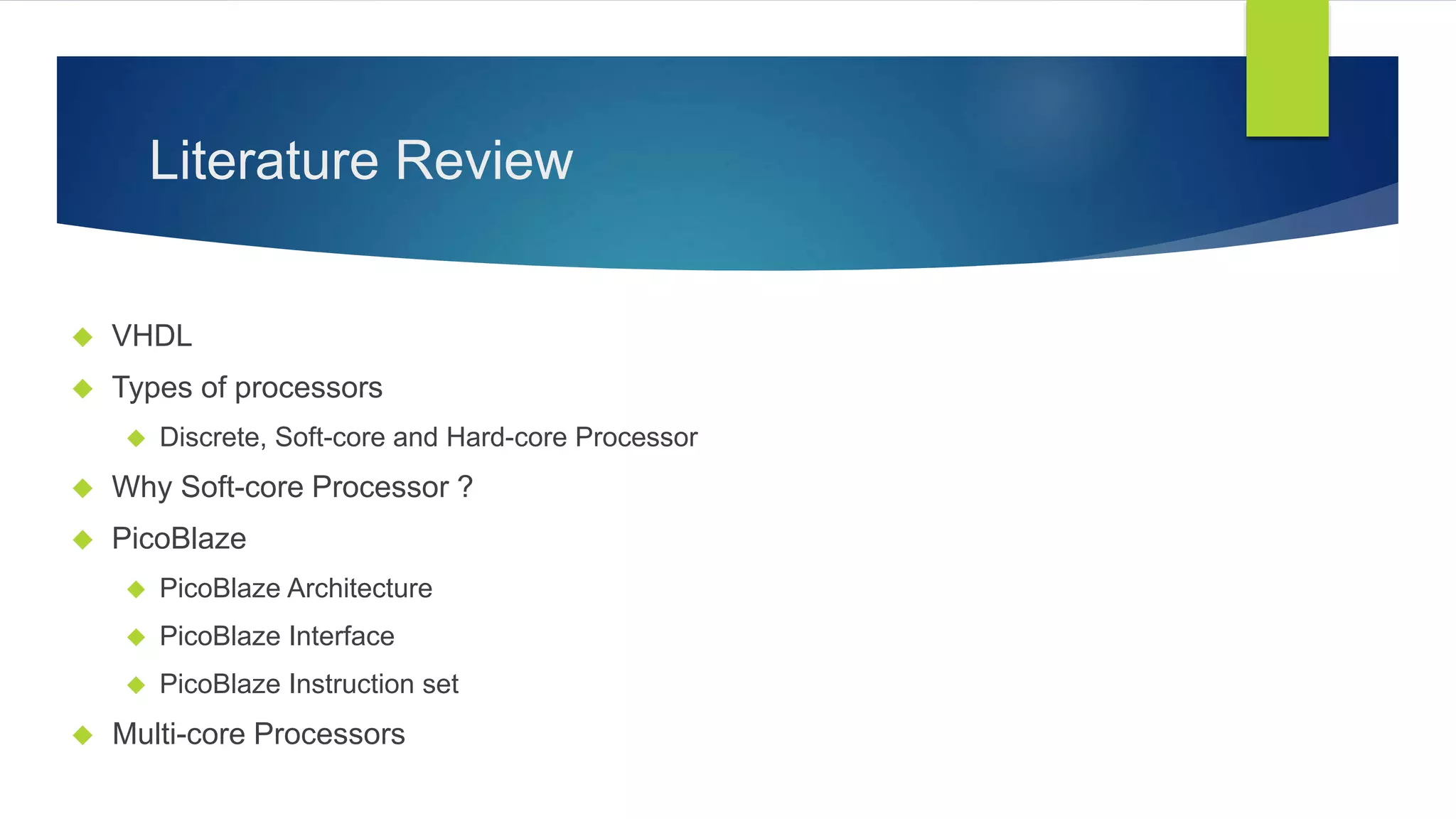
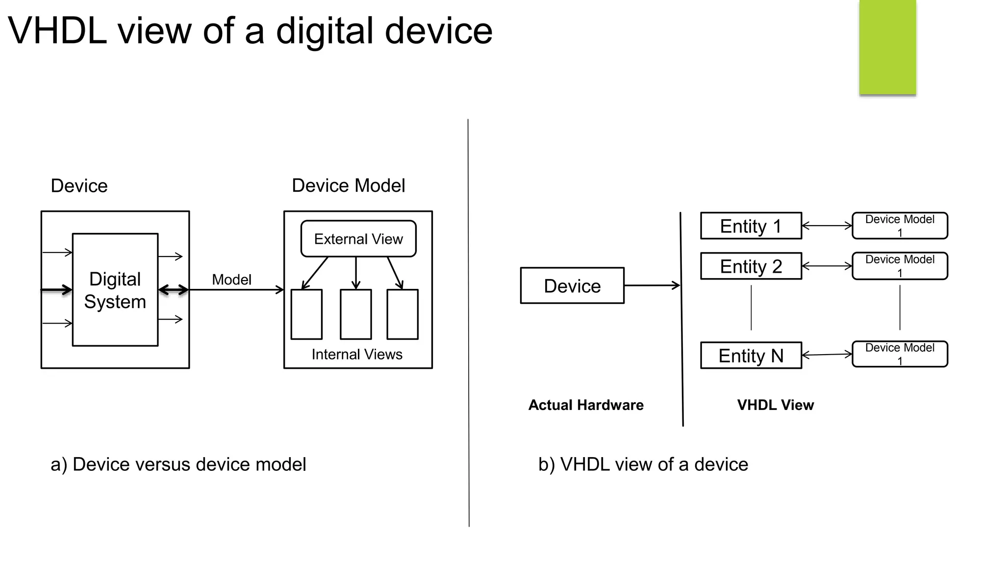
A Hardware Description Language that can be used to model a digital system.[1]
Three basic different description styles:
Structural
Dataflow
behavioural and
Combination of all is possible.
The language has constructs that enable you to express the concurrent or sequential
behaviour of a digital system with or without timing.
Easy & Simple](https://image.slidesharecdn.com/phaseii-140813232321-phpapp01/75/Implementation-of-Soft-core-processor-on-FPGA-Final-Presentation-5-2048.jpg)
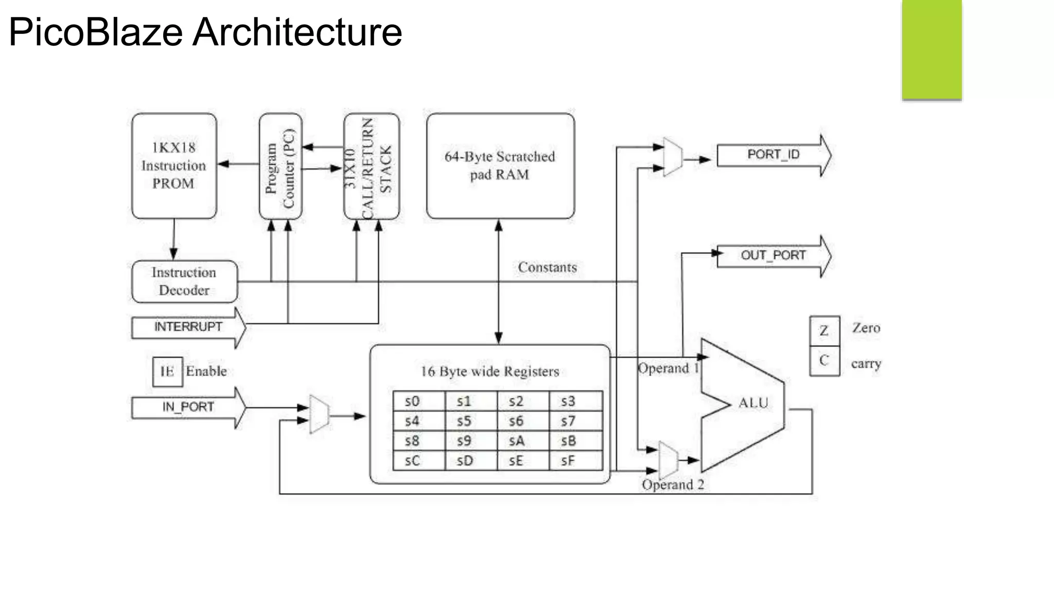
![PicoBlaze Microcontroller
Xilinx has developed two main Soft-cores:
MicroBlaze And PicoBlaze
The PicoBlaze is a compact, capable, and cost-effective fully embedded 8-bit RISC
microcontroller core optimized for the Xilinx FPGA families.[2]
The MicroBlaze is entirely implemented in general-purpose memory & logic fabrics of FPGA.
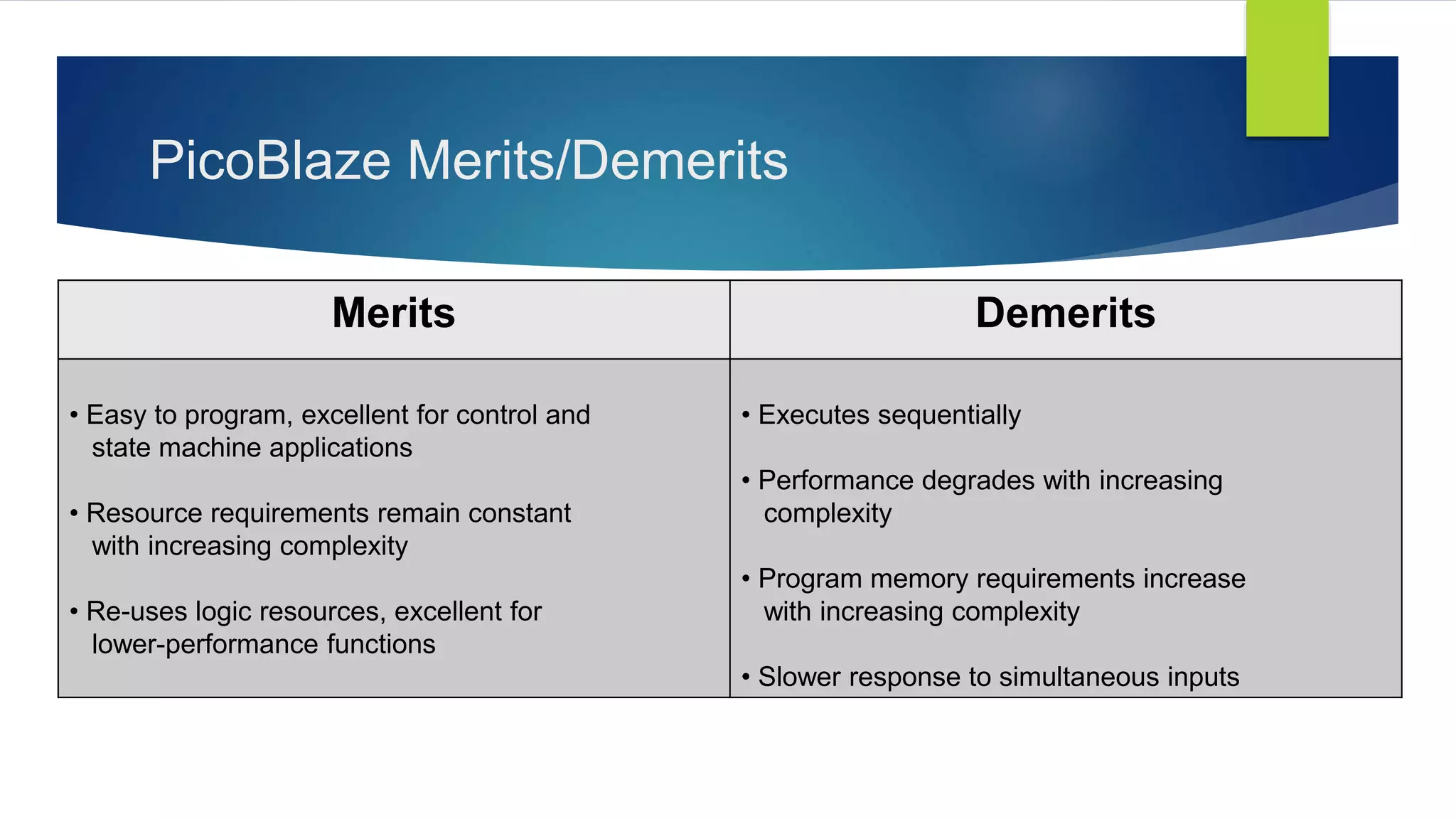
Features of PicoBlaze:
16 byte-wide general-purpose data registers
1K instructions of programmable on-chip program store
Byte-wide Arithmetic Logic Unit (ALU) with CARRY and ZERO indicator flags
256 input and 256 output ports & up to 240MHz performance](https://image.slidesharecdn.com/phaseii-140813232321-phpapp01/75/Implementation-of-Soft-core-processor-on-FPGA-Final-Presentation-9-2048.jpg)
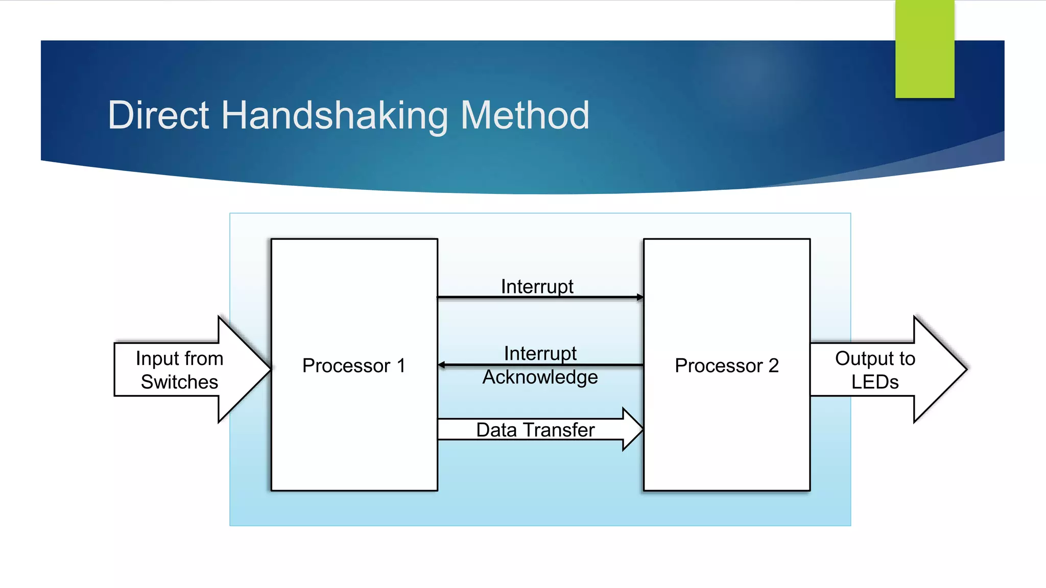
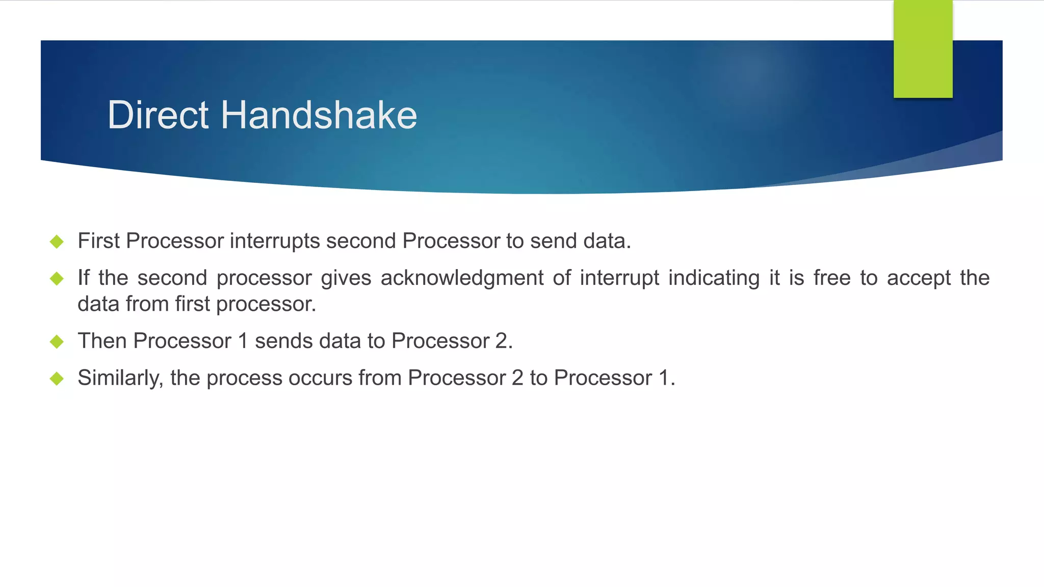
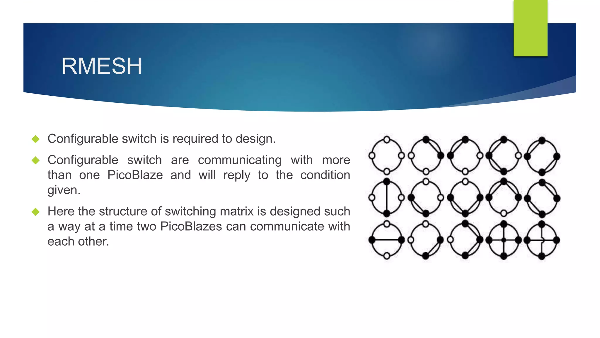
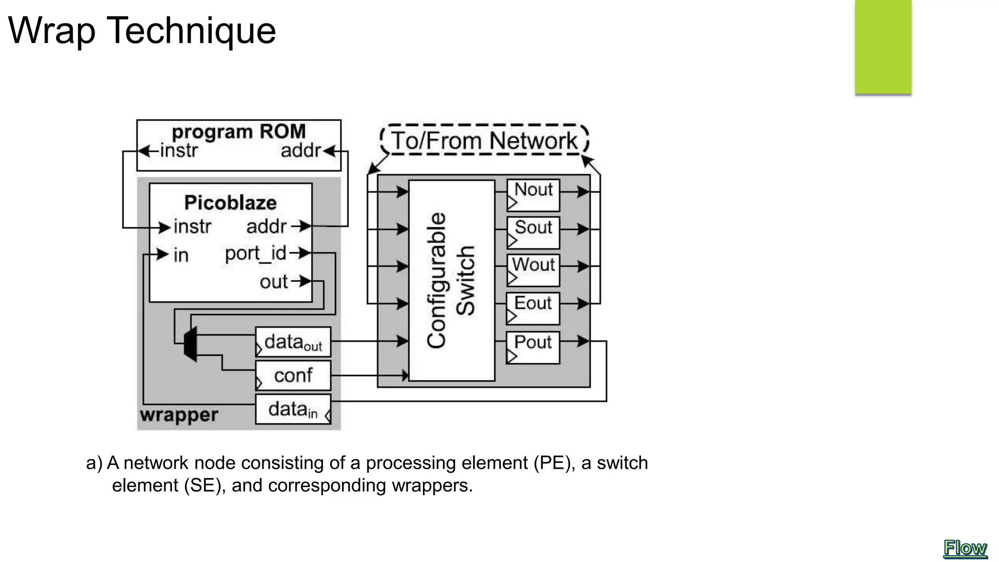
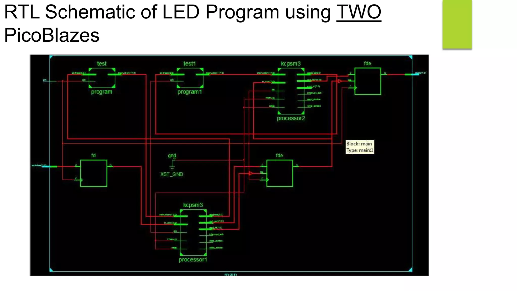
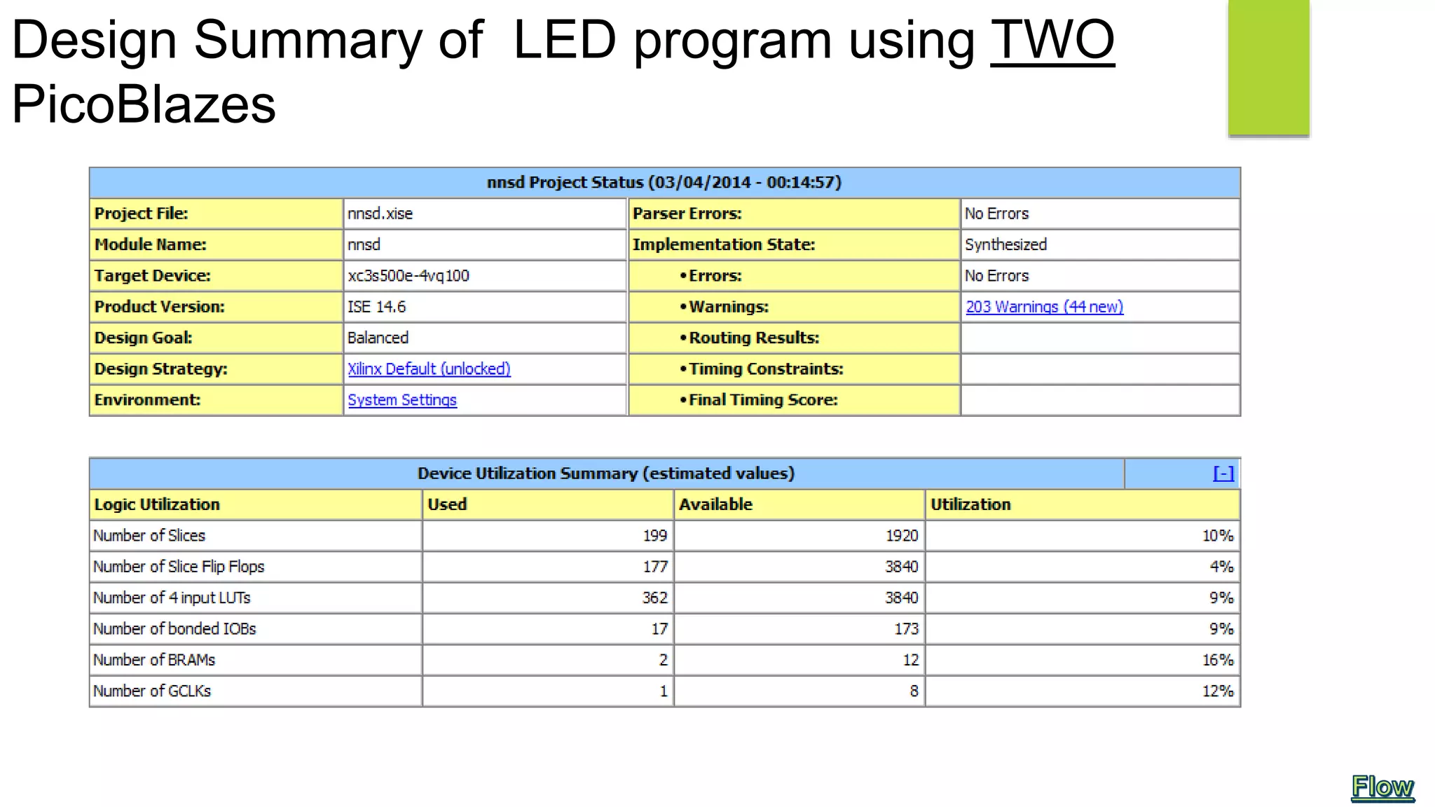
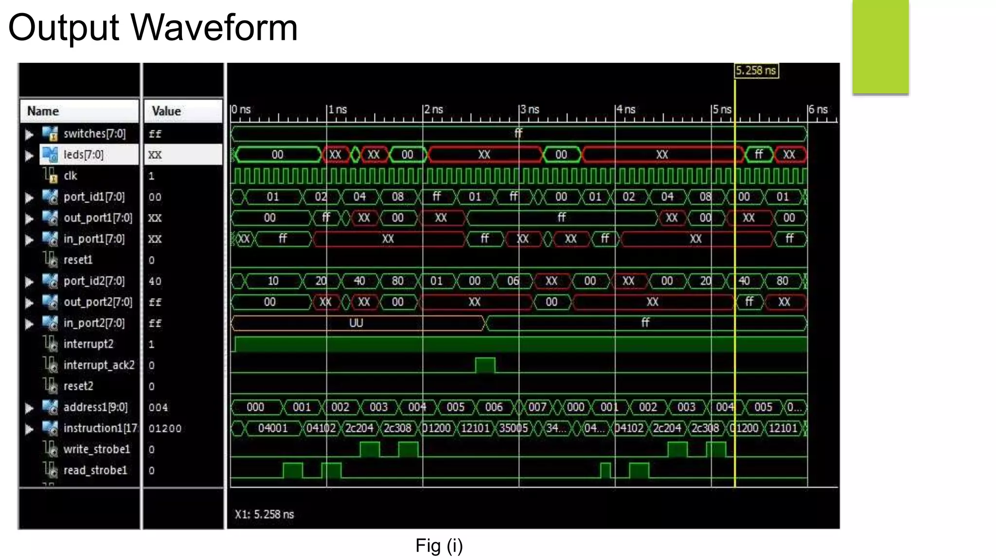
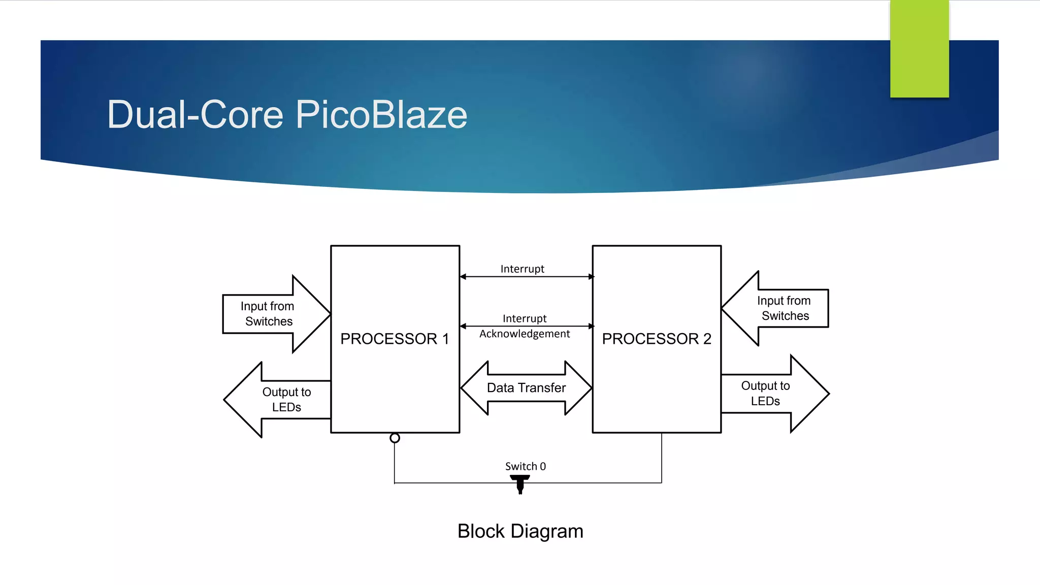
![Multi-core Processors
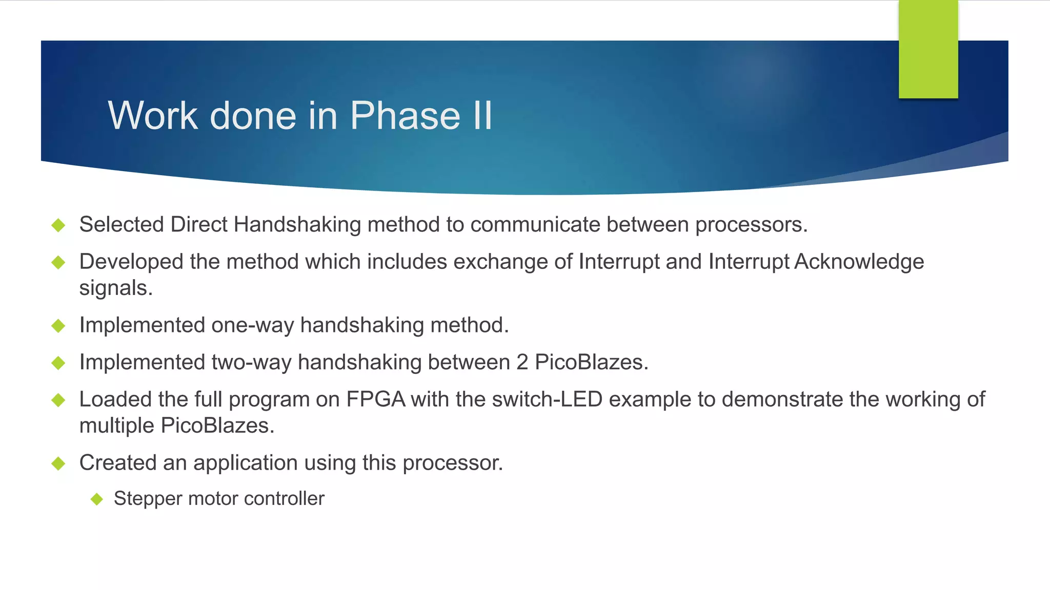
More than one PicoBlaze core can be implemented on FPGA and communication between
them can be made using any effective handshake technique.
The major Handshake Techniques are as follows:
Direct handshake
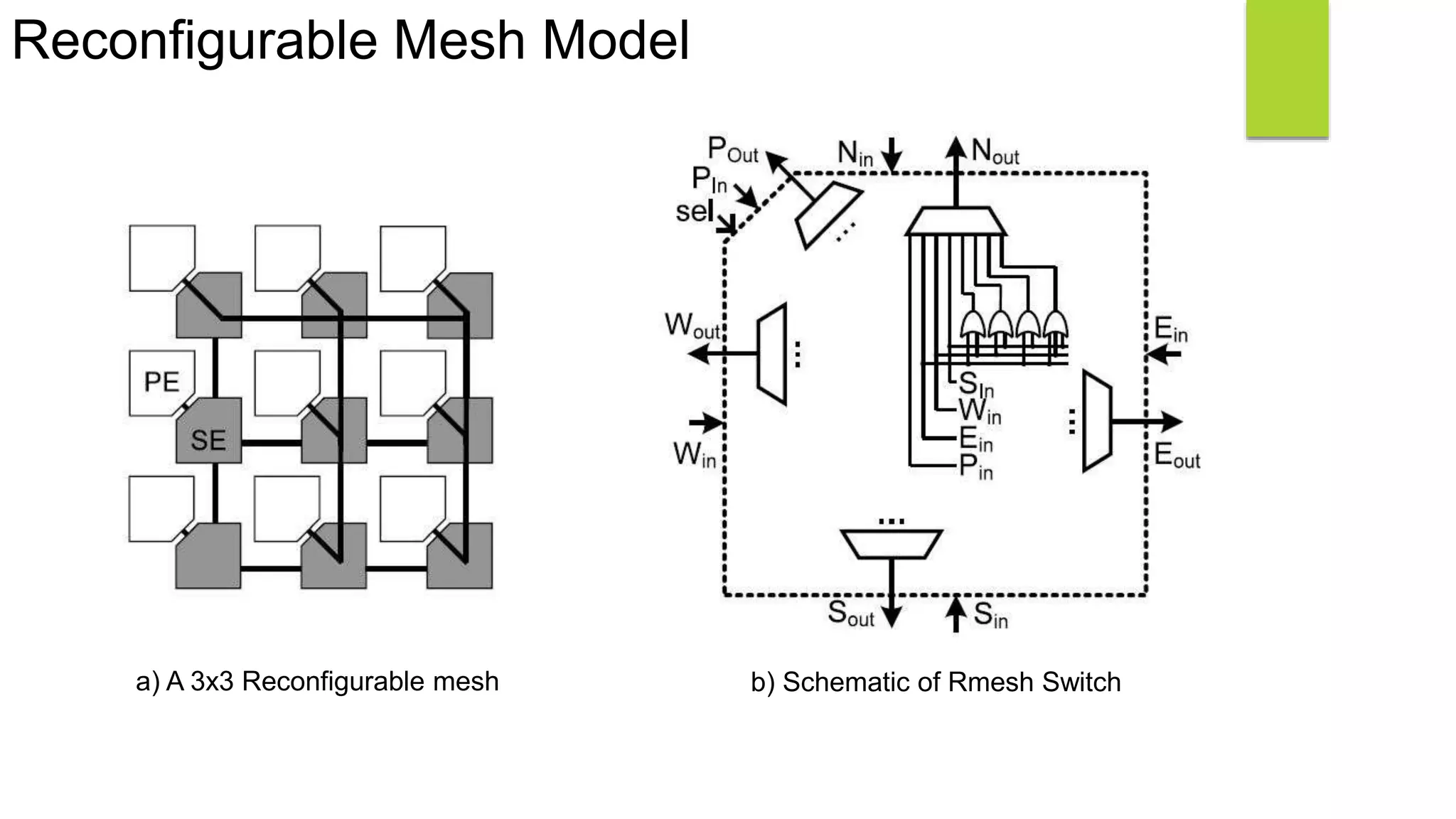
Handshake Based on Reconfigurable Mesh[8]
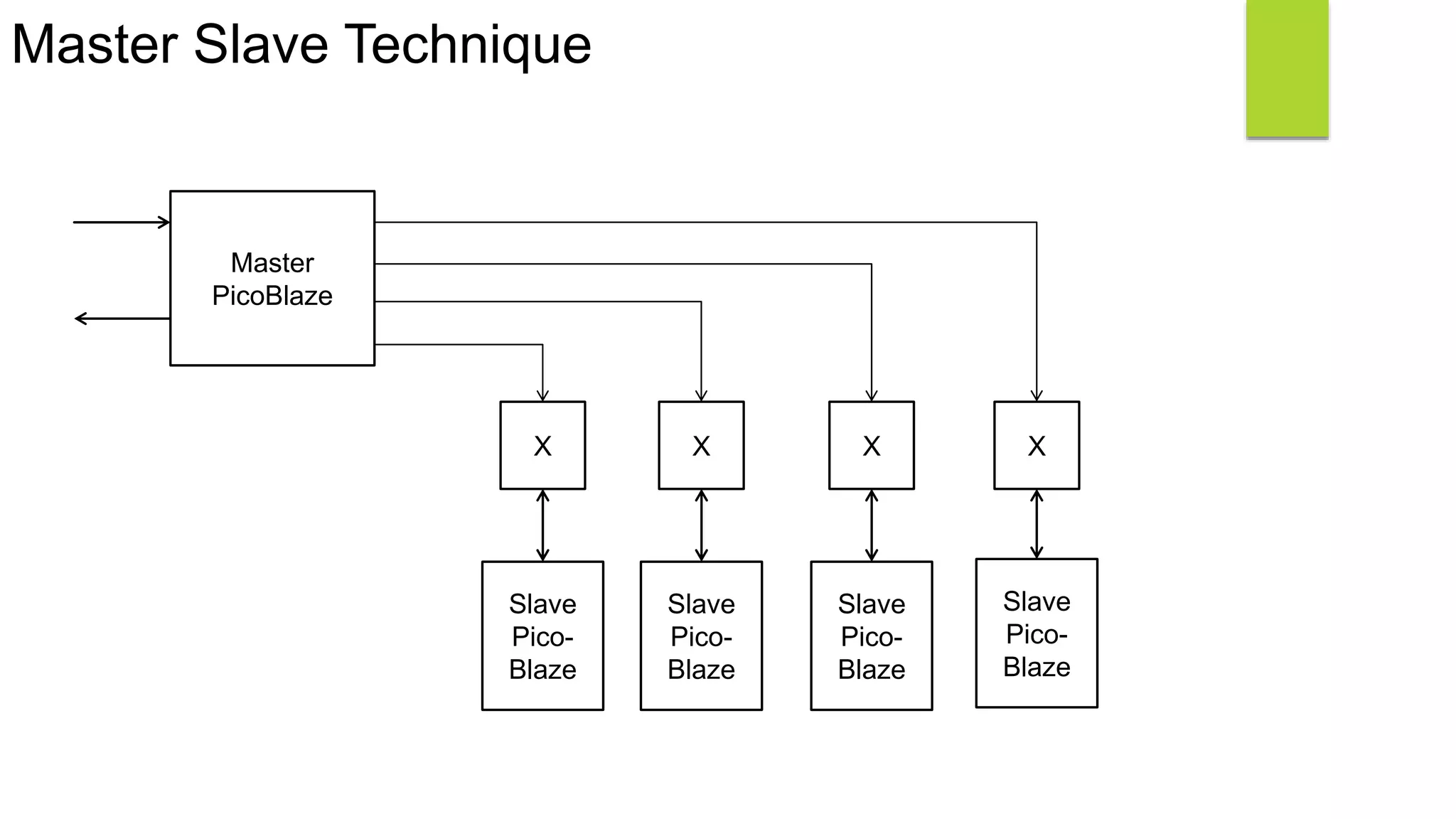
Master-Slave technique[7]
Wrap technique](https://image.slidesharecdn.com/phaseii-140813232321-phpapp01/75/Implementation-of-Soft-core-processor-on-FPGA-Final-Presentation-13-2048.jpg)
![Work Plan
Phase 1
Basic Study of VHDL.[1]
Literature Study of Soft-core processor.
Implementation of basic program in Xilinx & to observe their Waveform.
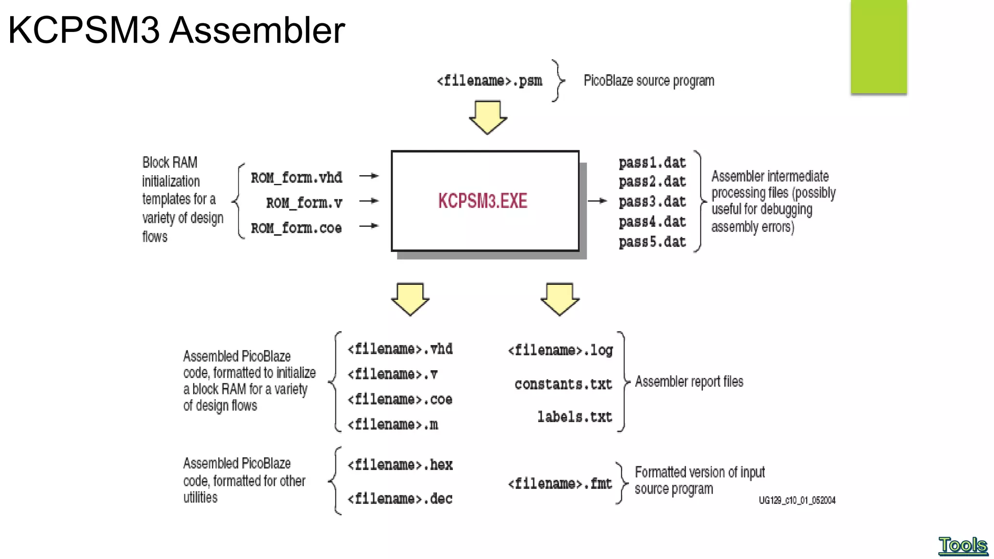
Basic study of KCPSM3 assembler.
Implementation of Soft-core in Xilinx.
To study different handshaking techniques between two processor.
Load basic program of PicoBlaze on Spartan-3e Board.](https://image.slidesharecdn.com/phaseii-140813232321-phpapp01/75/Implementation-of-Soft-core-processor-on-FPGA-Final-Presentation-28-2048.jpg)

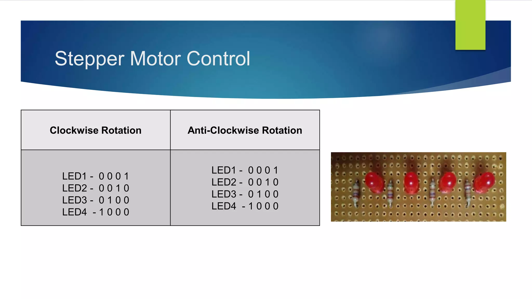

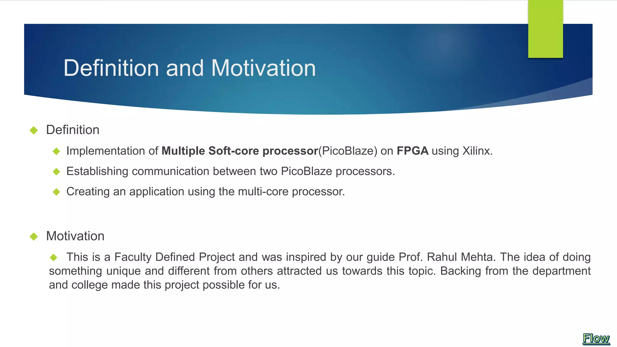
The document details the implementation of multiple soft-core processors, specifically Picoblaze, on FPGA using Xilinx technology, emphasizing the architecture, features, and communication techniques between processors. It covers VHDL as a modeling language, different types of processors, and handshaking methods for efficient data transfer. Additionally, it presents the work done in phases of the project, including the selection of techniques and successful interfacing of processors to create applications like a stepper motor controller.