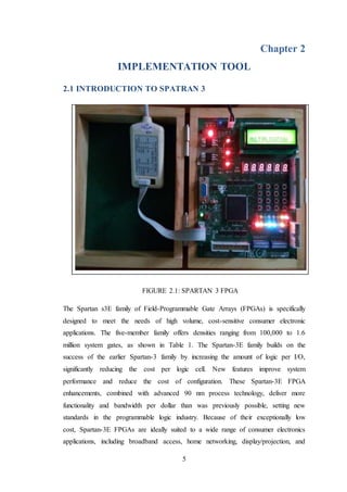
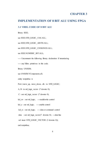
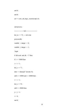
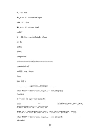
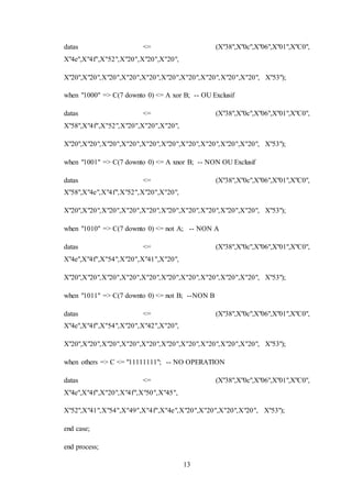
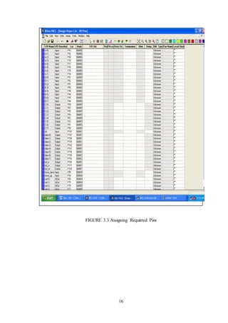
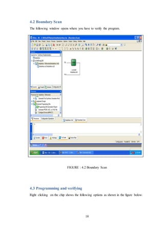
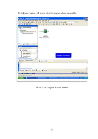
SlideShare a Scribd company logo
1 of 32
1
Chapter1
INTRODUCTION TO FPGA
1.1 INTRODUCTION
An FPGA is a device that contains a matrix of reconfigurable gate array logic
circuitry. When a FPGA is configured, the internal circuitry is connected in a way that
creates a hardware implementation of the software application. Unlike processors,
FPGAs use dedicated hardware for processing logic and do not have an operating
system. FPGAs are truly parallel in nature so different processing operations do not
have to compete for the same resources. As a result, the performance of one part of
the application is not affected when additional processing is added. Also, multiple
control loops can run on a single FPGA device at different rates. FPGA-based control
systems can enforce critical interlock logic and can be designed to prevent I/O forcing
by an operator. However, unlike hard-wired printed circuit board (PCB) designs
which have fixed hardware resources, FPGA-based systems can literally rewire their
internal circuitry to allow reconfiguration after the control system is deployed to the
field. FPGA devices deliver the performance and reliability of dedicated hardware
circuitry. A single FPGA can replace thousands of discrete components by
incorporating millions of logic gates in a single integrated circuit (IC) chip. The
internal resources of an FPGA chip consist of a matrix of configurable logic blocks
(CLBs) surrounded by a periphery of I/O blocks. Signals are routed within the FPGA
matrix by programmable interconnect switches and wire routes. The design and
implementation of FPGA based Arithmetic Logic Unit is of core significance in
digital technologies as it is an integral part of central processing unit. ALU is capable
of calculating the results of a wide variety of basic arithmetical and logical
computations. The ALU takes, as input, the data to be operated on (called operands)
and a code, from the control unit, indicating which operation to perform. The output is
the result of the computation. Designed ALU will perform the following operations:
• Arithmetic operations
• Bitwise logic operations
2
All the modules described in the design are coded using VHDL which is a very
useful tool with its degree of concurrency to cope with the parallelism of digital
hardware. The top level module connects all the stages into a higher level at Register
Transfer Logic (RTL). RTL describes the requirements of data and control units in
terms of digital logic to execute the desired operations. Each instruction from the
architecture's instruction set is defined in detail in the RTL Once identifying the
individual approaches for input, output and other modules, the VHDL descriptions are
run through a VHDL simulator and then is downloaded the design on FPGA board for
verification.
FIGURE 1.1: Internal Structure of FPGA
In an FPGA logic blocks are implemented using multiple level low fan-in gates,
which gives it a more compact design compared to an implementation with two-level
AND-OR logic. FPGA provides its user a way to configure:
1. The intersection between the logic blocks and
2. The function of each logic block.
Logic block of an FPGA can be configured in such a way that it can provide
functionality as simple as that of transistor or as complex as that of a microprocessor.
It can used to implement different combinations of combinational and sequential logic
functions. Logic blocks of an FPGA can be implemented by any of the following:
3
Transistor pairs, combinational gates like basic NAND gates or XOR gates, N -input
Lookup tables, Multiplexers, Wide fan-in And -OR structure.
Routing in FPGAs consists of wire segments of varying lengths which can be
interconnected via electrically programmable switches. Density of logic block used in
an FPGA depends on length and number of wire segments used for routing. Number
of segments used for interconnection typically is a tradeoff between density of logic
blocks used and amount of area used up for routing. Simplified version of FPGA
internal architecture with routing.
FIGURE 1.2: Simplified Internal Structure of FPGA
1.2 Why do we need FPGAs?
By the early 1980’s large scale integrated circuits (LSI) formed the back bone of most
of the logic circuits in major systems. Microprocessors, bus/IO controllers, system
timers were implemented using integrated circuit fabrication technology. Random
“glue logic” or interconnects were still required to help connect the large integrated
circuits in order to: 1. Generate global control signals (for resets etc.) 2. Data signals
from one subsystem to another sub system. Systems typically consisted of few large
scale integrated components and large number of SSI (small scale integrated circuit)
and MSI (medium scale integrated circuit) components. Initial attempt to solve this
problem led to development of Custom ICs which were to replace the large amount of
4
interconnect. This reduced system complexity and manufacturing cost, and improved
performance. However, custom ICs have their own disadvantages. They are relatively
very expensive to develop, and delay introduced for product to market (time to
market) because of increased design time. There are two kinds of costs involved in
development of custom ICs 1. Cost of development and design 2. Cost of manufacture
(A tradeoff usually exists between the two costs) Therefore the custom IC approach
was only viable for products with very high volume, and which were not time to
market sensitive. FPGAs were introduced as an alternative to custom ICs for
implementing entire system on one chip and to provide flexibility of re programibility
to the user. Introduction of FPGAs resulted in improvement of density relative to
discrete SSI/MSI components (within around 10x of custom ICs). Another advantage
of FPGAs over Custom ICs is that with the help of computer aided design (CAD)
tools circuits could be implemented in a short amount of time (no physical layout
process, no mask making, no IC manufacturing)
5
Chapter 2
IMPLEMENTATION TOOL
2.1 INTRODUCTION TO SPATRAN 3
FIGURE 2.1: SPARTAN 3 FPGA
The Spartan s3E family of Field-Programmable Gate Arrays (FPGAs) is specifically
designed to meet the needs of high volume, cost-sensitive consumer electronic
applications. The five-member family offers densities ranging from 100,000 to 1.6
million system gates, as shown in Table 1. The Spartan-3E family builds on the
success of the earlier Spartan-3 family by increasing the amount of logic per I/O,
significantly reducing the cost per logic cell. New features improve system
performance and reduce the cost of configuration. These Spartan-3E FPGA
enhancements, combined with advanced 90 nm process technology, deliver more
functionality and bandwidth per dollar than was previously possible, setting new
standards in the programmable logic industry. Because of their exceptionally low
cost, Spartan-3E FPGAs are ideally suited to a wide range of consumer electronics
applications, including broadband access, home networking, display/projection, and
6
digital television equipment. The Spartan-3E family is a superior alternative to mask
programmed ASICs. FPGAs avoid the high initial cost, the lengthy development
cycles, and the inherent inflexibility of conventional ASICs. Also, FPGA
programmability permits design upgrades in the field with no hardware replacement
necessary, an impossibility with ASICs.
2.2 POWER SUPPLY
The power supply to FPGA is given through the port shown below
FIGURE 2.2: Power Cable
2.3 JTAG CABLE
Joint Text Action Loop Cable is used to transfer the data into the FPGA where it is to
be burnt and verified.
7
FIGURE 2.3: JTAG Cable
2.4 Spartan 3 Pin Configuration
XC3S400_PQ208 is the main IC in the FPGA and has 208 pins ,52 on each side. The
figure below shows the pin configuration.
FIGURE 2.4 : XC3S400_PQ208 Pin Configuration
8
CHAPTER 3
IMPLEMENTATION OF 8 BIT ALU USING FPGA
3.1 VHDL CODE OF 8 BIT ALU
library IEEE;
use IEEE.STD_LOGIC_1164.ALL;
use IEEE.STD_LOGIC_ARITH.ALL;
use IEEE.STD_LOGIC_UNSIGNED.ALL;
use IEEE.NUMERIC_BIT.ALL;
---- Uncomment the following library declaration if instantiating
---- any Xilinx primitives in this code.
library UNISIM;
use UNISIM.VComponents.all;
entity testpinbus is
Port ( move_up, move_down, clk : in STD_LOGIC;
A, B : in std_logic_vector (7 downto 0);
C : out std_logic_vector (7 downto 0);
lcd_rw : out std_logic; ---read&write control
lcd_e : out std_logic; ----enable control
lcd_rs : out std_logic; ----data or command control
data : out std_logic_vector(7 downto 0); ---data line
sel: inout STD_LOGIC_VECTOR (3 downto 0));
end testpinbus;
9
architecture Behavioral of testpinbus is
signal c1 : integer range 0 to 350000;
constant N: integer :=22;
type arr is array (1 to N) of std_logic_vector(7 downto 0);
signaldatas:arr:=(X"38",X"0c",X"06",X"01",X"C0",X"57",X"45",X"4c",X"43",X"4f"
,X"4d",X"45",X"20",X"20",X"20",X"20",X"20",X"20",X"20",X"20",X"20", X"53");
--command and data to display;
begin
process (clk)
variable temp1 : integer range 0 to 15;
begin
if(rising_edge(clk))then
if move_up = '0' then
c1 <= c1 + 1;
if (c1 = 350000) then
temp1 := temp1 + 1;
end if;
elsif move_down = '0' then
c1 <= c1 + 1;
if (c1 = 350000) then
temp1 := temp1 - 1;
end if;
10
end if;
end if;
sel <= conv_std_logic_vector(temp1,4);
end process;
----------------lcd-------------------
lcd_rw <= '0'; ----lcd write
process(clk)
variable i : integer := 0;
variable j : integer := 1;
begin
if clk'event and clk = '1' then
if i <= 10000 then
i := i + 1;
lcd_e <= '1';
data <= datas(j)(7 downto 0);
elsif i > 10000 and i < 20000 then
i := i + 1;
lcd_e <= '0';
elsif i = 20000 then
j := j + 1;
i := 0;
end if;
11
if j <= 5 then
lcd_rs <= '0'; ---command signal
elsif j > 5 then
lcd_rs <= '1'; ----data signal
end if;
if j = 22 then ---repeated display of data
j := 5;
end if;
end if;
end process;
---------------------selecteur---------------------
process (a,b,sel)
variable temp : integer;
begin
case SEL is
------------------Opérations Arithmétiques-----------
when "0001" => temp := conv_integer(A) + conv_integer(B); --
Addition;
C <= conv_std_logic_vector(temp,8);
datas <= (X"38",X"0c",X"06",X"01",X"C0",
X"41",X"44",X"44",X"49",X"54",X"49",
X"4f",X"4e",X"20",X"20",X"20",X"20", X"20",X"20",X"20",X"20", X"53");
when "0010" => temp := conv_integer(A) - conv_integer(B); -
subtraction
12
C <= conv_std_logic_vector(temp,8);
datas <= (X"38",X"0c",X"06",X"01",X"C0",
X"53",X"55",X"42",X"54",X"52",X"41",
X"43",X"54",X"49",X"4f",X"4e",X"20",X"20",X"20",X"20",X"20", X"53");
when "0011" => temp := conv_integer(A) * conv_integer(B); --
Multiplication;
C <= conv_std_logic_vector(temp,8);
datas <= (X"38",X"0c",X"06",X"01",X"C0",
X"4d",X"55",X"4c",X"54",X"49",X"50",
X"4c",X"49",X"43",X"41",X"54",X"49",X"4f",X"4e",X"20",X"20", X"53");
---------------------Opérations Logiques-------------
when "0100" => C(7 downto 0) <= A and B; -- ET
datas <= (X"38",X"0c",X"06",X"01",X"C0",
X"41",X"4e",X"44",X"20",X"20",X"20",X"20",X"20",X"20",X"20",X"20",X"20",X"
20",X"20",X"20",X"20", X"53");
when "0101" => C(7 downto 0) <= A nand B; -- NON ET
datas <= (X"38",X"0c",X"06",X"01",X"C0",
X"4e",X"41",X"4e",X"44",X"20",X"20",
X"20",X"20",X"20",X"20",X"20",X"20",X"20",X"20",X"20",X"20", X"53");
when "0110" => C(7 downto 0) <= A or B; -- OU
datas <= (X"38",X"0c",X"06",X"01",X"C0",
X"4f",X"52",X"20",X"20",X"20",X"20",
X"20",X"20",X"20",X"20",X"20",X"20",X"20",X"20",X"20",X"20", X"53");
when "0111" => C(7 downto 0) <= A nor B; -- NON OU
13
datas <= (X"38",X"0c",X"06",X"01",X"C0",
X"4e",X"4f",X"52",X"20",X"20",X"20",
X"20",X"20",X"20",X"20",X"20",X"20",X"20",X"20",X"20",X"20", X"53");
when "1000" => C(7 downto 0) <= A xor B; -- OU Exclusif
datas <= (X"38",X"0c",X"06",X"01",X"C0",
X"58",X"4f",X"52",X"20",X"20",X"20",
X"20",X"20",X"20",X"20",X"20",X"20",X"20",X"20",X"20",X"20", X"53");
when "1001" => C(7 downto 0) <= A xnor B; -- NON OU Exclusif
datas <= (X"38",X"0c",X"06",X"01",X"C0",
X"58",X"4e",X"4f",X"52",X"20",X"20",
X"20",X"20",X"20",X"20",X"20",X"20",X"20",X"20",X"20",X"20", X"53");
when "1010" => C(7 downto 0) <= not A; -- NON A
datas <= (X"38",X"0c",X"06",X"01",X"C0",
X"4e",X"4f",X"54",X"20",X"41",X"20",
X"20",X"20",X"20",X"20",X"20",X"20",X"20",X"20",X"20",X"20", X"53");
when "1011" => C(7 downto 0) <= not B; --NON B
datas <= (X"38",X"0c",X"06",X"01",X"C0",
X"4e",X"4f",X"54",X"20",X"42",X"20",
X"20",X"20",X"20",X"20",X"20",X"20",X"20",X"20",X"20",X"20", X"53");
when others => C <= "11111111"; -- NO OPERATION
datas <= (X"38",X"0c",X"06",X"01",X"C0",
X"4e",X"4f",X"20",X"4f",X"50",X"45",
X"52",X"41",X"54",X"49",X"4f",X"4e",X"20",X"20",X"20",X"20", X"53");
end case;
end process;
14
end Behavioral;
3.2 IMPLEMENTATION IN VHDL
After writing the VHDL code and saving successfully various steps are to be followed
such as
3.1.1 Check Syntax
In the process window click on synthesize –XST which performs the checkin of errors
and shows warnings if any in the written code.
FIGURE 3.1 : Check Syntax
3.1.2 Generating Programming File
In Generate Programming File the bit file gets generated as shown in the figure
below.
15
FIGURE 3.2 : Generating Programming File
3.1.3 Assigning Required Pins
We need to assign the pins in the following window . The pins could be Input ,Output
Clock etc. There are 16 input and 16 output pins in the Spartan 3 FPGA.
16
FIGURE 3.3 Assigning Requirred Pins
17
CHAPTER 4
PROGRAMMING AND BURNING
4.1 Configure Device IMPACT
It is the last step before the boundary scan where the code (program) has to be
verified and programmed. Keep in mind to connect the FPGA device before
performing this step through JTAG cable and power supply cable.
FIGURE 4.1 : Configure Device IMPACT
18
4.2 Boundary Scan
The following window opens where you have to verify the program.
FIGURE : 4.2 Boundary Scan
4.3 Programming and verifying
Right clicking on the chip shows the following options as shown in the figure below.
19
FIGURE : 4.3 Programming and verifying
Click on the program and following window will appear which shows the burning of
the program.
FIGURE 4.4: Progress Dialogue
20
The following window will appear when the program is burnt successfully.
FIGURE 4.4 : Program Succeed window
21
CHAPTER 5
RESULT
Let the input A = 00010100 and B=01010001
Performing the arithmetic and logic operations on FPGA we get the following results.
5.1 Multiplication
Multiplying A= 00010100 and B = 01010001 we get 001000110 as output as shown
in figure below
FIGURE 5.1: Multiplication
22
5.2 Addition
Performing the addition between A =00010100 and B= 01010001 the result is
01111001 as shown in below figure.
FIGURE 5.2 : Addition
5.3 Subtraction
Subtracting A= 00010100 and B=01111001 the result is 00011001 as shown below in
the figure.
23
FIGURE 5.3 : Subtraction
5.4 AND Operation
Performing AND operation between A=00010100 and B= 01010001 the result is
01010001as shown in figure below
24
FIGURE 5.4 : AND Operation
5.5 OR Operation
Performing the OR Operation between A=00010100 and B= 01010001 the result is
11010011 as shown in figure below.
25
FIGURE 5.5 : OR Operation
5.5 NAND Operation
The result of performing NAND operation between A= 00010100 and B= 01010001
is 10101010as in figure below
26
FIGURE 5.5 : NAND Operation
5.6 NOR Operation
The result of performing NOR operation between A= 10100 and B= 01010001 is
00001000 as in below figure.
27
FIGURE 5.6 : NOR Operation
5.7 XOR Operation
Performing XOR Operation between A= 00010100 and B= 01010001 we get
10100110 as result
28
FIGURE 5.7 : XOR Operation
5.8 XNOR Operation
Performing XNOR Operation between A=00010100 and B=01010001 we get
01011001 as result
29
FIGURE 5.8 : XNOR Operation
5.9 NO OPERATION
When A=11111111 and B=11111111 the LCD shows NO OPERATION as shown
below
30
FIGURE 5.9 : NO OPERATION
31
Chapter 6
CONCLUSION
This study helped to understand the complete flow of RTL design, starting from
designing a top level RTL module for 8-bit ALU using hardware description
language, VHDL. Verification of the designed RTL code using simulation techniques,
synthesis of RTL code to obtain gate level netlist using Xilinx ISE tool and
Arithmetic Logic Unit was successfully designed and implemented using Very High
Speed Hardware Descriptive Language and Xilinx Spatan-3E Field Programmable
Gate Array. VHDL implementation of 8-bit arithmetic logic unit (ALU) is presented.
The design was implemented using VHDL Xilinx Synthesis tool ISE 13.1 and
targeted for Spartan device. ALU was designed to perform arithmetic operations such
as addition and subtraction using 8-bit fast adder, logical operations such as AND,
OR, XOR and NOT operations, 1’s and 2’s complement operations and compare. The
maximum propagation delay is 13.588ns and power dissipation is 38mW. The ALU
was designed for controller used in network interface card.
32
REFRENCES
[1] Toshio Fujisawa, et al, “A Single-Chip 802.11a MAC/PHY With a 32-b RISC
Processor”, in IEEE Journal Of Solid-State Circuits, Vol. 38, No. 11, November 2003.
[2] J. R. Allen, et al, “IBM PowerNP network processor: Hardware, software, and
applications,” in IBM Journal of Research & Development, Vol. 47, No. 2/3
March/May 2003.
[3] Xiaoning Nie, et al, “A New Network Processor Architecture for High-speed
Communications,” in IEEE Workshop on Signal Processing Systems, 1999.
[4] H. Peter Hofstee, “Power Efficient Processor Architecture and The Cell
Processor,” in Proceedings of the 11th International Symposium on High-
Performance Computer Architecture, 2005.
[5] D. L. Perry, “ VHDL”, Tata Mcgraw Hill Edition, 4th Edition, 2002.
[6] C. Maxfiled, “The Design Warriors Guide to FPGAs”, Elsevier, 2004.
[7] J. Bhaskar, “ VHDL Primer”, Pearson Education, 3rd Edition, 2000.
[8] J. Bhaskar, “ VHDL Synthesis Primer”, Pearson Education, 1st Edition, 2002.

More Related Content

What's hot

Session 2,3 FPGAs
Session 2,3 FPGAsSession 2,3 FPGAs
Session 2,3 FPGAsSubhash Iyer
 
Fpga(field programmable gate array)
Fpga(field programmable gate array) Fpga(field programmable gate array)
Fpga(field programmable gate array) Iffat Anjum
 
Cpld and fpga mod vi
Cpld and fpga   mod viCpld and fpga   mod vi
Cpld and fpga mod viAgi George
 
Implementation of Soft-core processor on FPGA (Final Presentation)
Implementation of Soft-core processor on FPGA (Final Presentation)Implementation of Soft-core processor on FPGA (Final Presentation)
Implementation of Soft-core processor on FPGA (Final Presentation)Deepak Kumar
 
Spartan-II FPGA (xc2s30)
Spartan-II FPGA (xc2s30)Spartan-II FPGA (xc2s30)
Spartan-II FPGA (xc2s30)A B Shinde
 
Cpld fpga
Cpld fpgaCpld fpga
Cpld fpgaanishgoel
 
Iaetsd a design of fpga with ledr encoding and
Iaetsd a design of fpga with ledr encoding andIaetsd a design of fpga with ledr encoding and
Iaetsd a design of fpga with ledr encoding andIaetsd Iaetsd
 
Fpga optimus main_print
Fpga optimus  main_printFpga optimus  main_print
Fpga optimus main_printSushant Burde
 
CPLD xc9500
CPLD xc9500CPLD xc9500
CPLD xc9500A B Shinde
 
Fpga Knowledge
Fpga KnowledgeFpga Knowledge
Fpga Knowledgeranvirsingh
 
FPGA TECHNOLOGY AND FAMILIES
FPGA TECHNOLOGY AND FAMILIESFPGA TECHNOLOGY AND FAMILIES
FPGA TECHNOLOGY AND FAMILIESrevathilakshmi2
 

What's hot (20)

Session 2,3 FPGAs
Session 2,3 FPGAsSession 2,3 FPGAs
Session 2,3 FPGAs
 
Fpga(field programmable gate array)
Fpga(field programmable gate array) Fpga(field programmable gate array)
Fpga(field programmable gate array)
 
Cpld and fpga mod vi
Cpld and fpga   mod viCpld and fpga   mod vi
Cpld and fpga mod vi
 
FPGA
FPGAFPGA
FPGA
 
Implementation of Soft-core processor on FPGA (Final Presentation)
Implementation of Soft-core processor on FPGA (Final Presentation)Implementation of Soft-core processor on FPGA (Final Presentation)
Implementation of Soft-core processor on FPGA (Final Presentation)
 
FPGA
FPGAFPGA
FPGA
 
Spartan-II FPGA (xc2s30)
Spartan-II FPGA (xc2s30)Spartan-II FPGA (xc2s30)
Spartan-II FPGA (xc2s30)
 
Cpld fpga
Cpld fpgaCpld fpga
Cpld fpga
 
Fpga intro1
Fpga intro1Fpga intro1
Fpga intro1
 
Fpga
FpgaFpga
Fpga
 
FPGA In a Nutshell
FPGA In a NutshellFPGA In a Nutshell
FPGA In a Nutshell
 
Iaetsd a design of fpga with ledr encoding and
Iaetsd a design of fpga with ledr encoding andIaetsd a design of fpga with ledr encoding and
Iaetsd a design of fpga with ledr encoding and
 
Fpga
FpgaFpga
Fpga
 
Fpga 03-cpld-and-fpga
Fpga 03-cpld-and-fpgaFpga 03-cpld-and-fpga
Fpga 03-cpld-and-fpga
 
Fpga optimus main_print
Fpga optimus  main_printFpga optimus  main_print
Fpga optimus main_print
 
CPLD xc9500
CPLD xc9500CPLD xc9500
CPLD xc9500
 
Fpga Knowledge
Fpga KnowledgeFpga Knowledge
Fpga Knowledge
 
Fpga & VHDL
Fpga & VHDLFpga & VHDL
Fpga & VHDL
 
CPLDs
CPLDsCPLDs
CPLDs
 
FPGA TECHNOLOGY AND FAMILIES
FPGA TECHNOLOGY AND FAMILIESFPGA TECHNOLOGY AND FAMILIES
FPGA TECHNOLOGY AND FAMILIES
 

Viewers also liked

Nano technology 3 acknowledgement
Nano technology 3 acknowledgementNano technology 3 acknowledgement
Nano technology 3 acknowledgementRameez Raja
 
5 g 4 abstract
5 g 4 abstract5 g 4 abstract
5 g 4 abstractRameez Raja
 
Fpg as 1 first page
Fpg as 1 first page Fpg as 1 first page
Fpg as 1 first page Rameez Raja
 
Camera surveilance 6 list of figures
Camera surveilance 6 list of figuresCamera surveilance 6 list of figures
Camera surveilance 6 list of figuresRameez Raja
 
Nano technology 4 contents
Nano technology 4 contentsNano technology 4 contents
Nano technology 4 contentsRameez Raja
 
Camera surveilance 1 front pg
Camera surveilance 1 front pgCamera surveilance 1 front pg
Camera surveilance 1 front pgRameez Raja
 
Dth 2certificate
Dth 2certificateDth 2certificate
Dth 2certificateRameez Raja
 
Dth 3 acknowledgement
Dth 3 acknowledgementDth 3 acknowledgement
Dth 3 acknowledgementRameez Raja
 
Plc 1 first page plc
Plc 1 first page plcPlc 1 first page plc
Plc 1 first page plcRameez Raja
 
5 g 3 acknowledgement
5 g 3 acknowledgement5 g 3 acknowledgement
5 g 3 acknowledgementRameez Raja
 
Camera surveilance 5 contents
Camera surveilance 5 contentsCamera surveilance 5 contents
Camera surveilance 5 contentsRameez Raja
 
Plc 6 list of figures plc
Plc 6 list of figures  plcPlc 6 list of figures  plc
Plc 6 list of figures plcRameez Raja
 
Nano technology 2 certificate
Nano technology 2 certificateNano technology 2 certificate
Nano technology 2 certificateRameez Raja
 
Camera surveilance 2certificate
Camera surveilance 2certificateCamera surveilance 2certificate
Camera surveilance 2certificateRameez Raja
 
Camera surveilance 3 acknowledgement
Camera surveilance 3 acknowledgementCamera surveilance 3 acknowledgement
Camera surveilance 3 acknowledgementRameez Raja
 
Dth 4 abstract
Dth 4 abstractDth 4 abstract
Dth 4 abstractRameez Raja
 
5 g 6 list of figures
5 g 6 list of figures5 g 6 list of figures
5 g 6 list of figuresRameez Raja
 
2certificate
2certificate2certificate
2certificateRameez Raja
 
5 g 2 certificate
5 g 2 certificate5 g 2 certificate
5 g 2 certificateRameez Raja
 
3 acknowledgement (2)
3 acknowledgement (2)3 acknowledgement (2)
3 acknowledgement (2)Rameez Raja
 

Viewers also liked (20)

Nano technology 3 acknowledgement
Nano technology 3 acknowledgementNano technology 3 acknowledgement
Nano technology 3 acknowledgement
 
5 g 4 abstract
5 g 4 abstract5 g 4 abstract
5 g 4 abstract
 
Fpg as 1 first page
Fpg as 1 first page Fpg as 1 first page
Fpg as 1 first page
 
Camera surveilance 6 list of figures
Camera surveilance 6 list of figuresCamera surveilance 6 list of figures
Camera surveilance 6 list of figures
 
Nano technology 4 contents
Nano technology 4 contentsNano technology 4 contents
Nano technology 4 contents
 
Camera surveilance 1 front pg
Camera surveilance 1 front pgCamera surveilance 1 front pg
Camera surveilance 1 front pg
 
Dth 2certificate
Dth 2certificateDth 2certificate
Dth 2certificate
 
Dth 3 acknowledgement
Dth 3 acknowledgementDth 3 acknowledgement
Dth 3 acknowledgement
 
Plc 1 first page plc
Plc 1 first page plcPlc 1 first page plc
Plc 1 first page plc
 
5 g 3 acknowledgement
5 g 3 acknowledgement5 g 3 acknowledgement
5 g 3 acknowledgement
 
Camera surveilance 5 contents
Camera surveilance 5 contentsCamera surveilance 5 contents
Camera surveilance 5 contents
 
Plc 6 list of figures plc
Plc 6 list of figures  plcPlc 6 list of figures  plc
Plc 6 list of figures plc
 
Nano technology 2 certificate
Nano technology 2 certificateNano technology 2 certificate
Nano technology 2 certificate
 
Camera surveilance 2certificate
Camera surveilance 2certificateCamera surveilance 2certificate
Camera surveilance 2certificate
 
Camera surveilance 3 acknowledgement
Camera surveilance 3 acknowledgementCamera surveilance 3 acknowledgement
Camera surveilance 3 acknowledgement
 
Dth 4 abstract
Dth 4 abstractDth 4 abstract
Dth 4 abstract
 
5 g 6 list of figures
5 g 6 list of figures5 g 6 list of figures
5 g 6 list of figures
 
2certificate
2certificate2certificate
2certificate
 
5 g 2 certificate
5 g 2 certificate5 g 2 certificate
5 g 2 certificate
 
3 acknowledgement (2)
3 acknowledgement (2)3 acknowledgement (2)
3 acknowledgement (2)
 

Similar to Fpg as 11 body

Fpga lecture
Fpga lectureFpga lecture
Fpga lectureZhwan Rashid
 
Nt1310 Unit 5 Algorithm
Nt1310 Unit 5 AlgorithmNt1310 Unit 5 Algorithm
Nt1310 Unit 5 AlgorithmAngie Lee
 
Fundamentals of FPGA
Fundamentals of FPGAFundamentals of FPGA
Fundamentals of FPGAvelamakuri
 
Fpga based motor controller
Fpga based motor controllerFpga based motor controller
Fpga based motor controllerUday Wankar
 
Programmable logic controller performance enhancement by field programmable g...
Programmable logic controller performance enhancement by field programmable g...Programmable logic controller performance enhancement by field programmable g...
Programmable logic controller performance enhancement by field programmable g...ISA Interchange
 
Fpga architectures and applications
Fpga architectures and applicationsFpga architectures and applications
Fpga architectures and applicationsSudhanshu Janwadkar
 
FPGA Architecture and application
FPGA Architecture and application FPGA Architecture and application
FPGA Architecture and application ADARSHJKALATHIL
 
L12 programmable+logic+devices+(pld)
L12 programmable+logic+devices+(pld)L12 programmable+logic+devices+(pld)
L12 programmable+logic+devices+(pld)NAGASAI547
 
Project report of 2016 Trainee_final
Project report of 2016 Trainee_finalProject report of 2016 Trainee_final
Project report of 2016 Trainee_finalAkash Chowdhury
 
L12_PROGRAMMABLE+LOGIC+DEVICES+(PLD).ppt
L12_PROGRAMMABLE+LOGIC+DEVICES+(PLD).pptL12_PROGRAMMABLE+LOGIC+DEVICES+(PLD).ppt
L12_PROGRAMMABLE+LOGIC+DEVICES+(PLD).pptMikeTango5
 
Implementation of CAN on FPGA for Security Evaluation Purpose
Implementation of CAN on FPGA for Security Evaluation PurposeImplementation of CAN on FPGA for Security Evaluation Purpose
Implementation of CAN on FPGA for Security Evaluation PurposeIRJET Journal
 
AN DYNAMIC ENERGY MANAGEMENT ON FPGA FOR WIRELESS SENSOR NETWORK
AN DYNAMIC ENERGY MANAGEMENT ON FPGA FOR WIRELESS SENSOR NETWORKAN DYNAMIC ENERGY MANAGEMENT ON FPGA FOR WIRELESS SENSOR NETWORK
AN DYNAMIC ENERGY MANAGEMENT ON FPGA FOR WIRELESS SENSOR NETWORKcsijjournal
 
System designing and modelling using fpga
System designing and modelling using fpgaSystem designing and modelling using fpga
System designing and modelling using fpgaIAEME Publication
 
High speed customized serial protocol for IP integration on FPGA based SOC ap...
High speed customized serial protocol for IP integration on FPGA based SOC ap...High speed customized serial protocol for IP integration on FPGA based SOC ap...
High speed customized serial protocol for IP integration on FPGA based SOC ap...IJMER
 
A LIGHT WEIGHT VLSI FRAME WORK FOR HIGHT CIPHER ON FPGA
A LIGHT WEIGHT VLSI FRAME WORK FOR HIGHT CIPHER ON FPGAA LIGHT WEIGHT VLSI FRAME WORK FOR HIGHT CIPHER ON FPGA
A LIGHT WEIGHT VLSI FRAME WORK FOR HIGHT CIPHER ON FPGAIRJET Journal
 
Design and Implementation of FPGA Based Signal Processing Card
Design and Implementation of FPGA Based Signal Processing Card  Design and Implementation of FPGA Based Signal Processing Card
Design and Implementation of FPGA Based Signal Processing Card VLSICS Design
 

Similar to Fpg as 11 body (20)

Convolution
ConvolutionConvolution
Convolution
 
Fpga lecture
Fpga lectureFpga lecture
Fpga lecture
 
Nt1310 Unit 5 Algorithm
Nt1310 Unit 5 AlgorithmNt1310 Unit 5 Algorithm
Nt1310 Unit 5 Algorithm
 
Fundamentals of FPGA
Fundamentals of FPGAFundamentals of FPGA
Fundamentals of FPGA
 
Fpga based motor controller
Fpga based motor controllerFpga based motor controller
Fpga based motor controller
 
Programmable logic controller performance enhancement by field programmable g...
Programmable logic controller performance enhancement by field programmable g...Programmable logic controller performance enhancement by field programmable g...
Programmable logic controller performance enhancement by field programmable g...
 
FIELD PROGRAMMABLE GATE ARRAYS AND THEIR APPLICATIONS
FIELD PROGRAMMABLE GATE ARRAYS AND THEIR APPLICATIONSFIELD PROGRAMMABLE GATE ARRAYS AND THEIR APPLICATIONS
FIELD PROGRAMMABLE GATE ARRAYS AND THEIR APPLICATIONS
 
Chapter 4
Chapter 4Chapter 4
Chapter 4
 
Fpga architectures and applications
Fpga architectures and applicationsFpga architectures and applications
Fpga architectures and applications
 
FPGA Architecture and application
FPGA Architecture and application FPGA Architecture and application
FPGA Architecture and application
 
L12 programmable+logic+devices+(pld)
L12 programmable+logic+devices+(pld)L12 programmable+logic+devices+(pld)
L12 programmable+logic+devices+(pld)
 
Project report of 2016 Trainee_final
Project report of 2016 Trainee_finalProject report of 2016 Trainee_final
Project report of 2016 Trainee_final
 
L12_PROGRAMMABLE+LOGIC+DEVICES+(PLD).ppt
L12_PROGRAMMABLE+LOGIC+DEVICES+(PLD).pptL12_PROGRAMMABLE+LOGIC+DEVICES+(PLD).ppt
L12_PROGRAMMABLE+LOGIC+DEVICES+(PLD).ppt
 
Implementation of CAN on FPGA for Security Evaluation Purpose
Implementation of CAN on FPGA for Security Evaluation PurposeImplementation of CAN on FPGA for Security Evaluation Purpose
Implementation of CAN on FPGA for Security Evaluation Purpose
 
AN DYNAMIC ENERGY MANAGEMENT ON FPGA FOR WIRELESS SENSOR NETWORK
AN DYNAMIC ENERGY MANAGEMENT ON FPGA FOR WIRELESS SENSOR NETWORKAN DYNAMIC ENERGY MANAGEMENT ON FPGA FOR WIRELESS SENSOR NETWORK
AN DYNAMIC ENERGY MANAGEMENT ON FPGA FOR WIRELESS SENSOR NETWORK
 
4_BIT_ALU
4_BIT_ALU4_BIT_ALU
4_BIT_ALU
 
System designing and modelling using fpga
System designing and modelling using fpgaSystem designing and modelling using fpga
System designing and modelling using fpga
 
High speed customized serial protocol for IP integration on FPGA based SOC ap...
High speed customized serial protocol for IP integration on FPGA based SOC ap...High speed customized serial protocol for IP integration on FPGA based SOC ap...
High speed customized serial protocol for IP integration on FPGA based SOC ap...
 
A LIGHT WEIGHT VLSI FRAME WORK FOR HIGHT CIPHER ON FPGA
A LIGHT WEIGHT VLSI FRAME WORK FOR HIGHT CIPHER ON FPGAA LIGHT WEIGHT VLSI FRAME WORK FOR HIGHT CIPHER ON FPGA
A LIGHT WEIGHT VLSI FRAME WORK FOR HIGHT CIPHER ON FPGA
 
Design and Implementation of FPGA Based Signal Processing Card
Design and Implementation of FPGA Based Signal Processing Card  Design and Implementation of FPGA Based Signal Processing Card
Design and Implementation of FPGA Based Signal Processing Card
 

More from Rameez Raja

Dth 5 contents
Dth 5 contentsDth 5 contents
Dth 5 contentsRameez Raja
 
Dth 1 first page dth
Dth 1 first page dthDth 1 first page dth
Dth 1 first page dthRameez Raja
 
Fpg as 9 abstract
Fpg as 9 abstractFpg as 9 abstract
Fpg as 9 abstractRameez Raja
 
Fpg as 7 list of figures
Fpg as 7 list of figuresFpg as 7 list of figures
Fpg as 7 list of figuresRameez Raja
 
Fpg as 3 acknowledgement (2)
Fpg as 3 acknowledgement (2)Fpg as 3 acknowledgement (2)
Fpg as 3 acknowledgement (2)Rameez Raja
 
Fpg as 5 contents
Fpg as 5 contentsFpg as 5 contents
Fpg as 5 contentsRameez Raja
 
Nano technology 7 smnr report
Nano technology 7 smnr reportNano technology 7 smnr report
Nano technology 7 smnr reportRameez Raja
 
Nano technology 6 abstract
Nano technology 6 abstractNano technology 6 abstract
Nano technology 6 abstractRameez Raja
 
Nano technology 5 list of figures
Nano technology 5 list of figuresNano technology 5 list of figures
Nano technology 5 list of figuresRameez Raja
 
Nano technology 0 front
Nano technology 0 frontNano technology 0 front
Nano technology 0 frontRameez Raja
 
Nano technology 1 declaration
Nano technology 1 declarationNano technology 1 declaration
Nano technology 1 declarationRameez Raja
 
Camera surveilance presentation 150812044730-lva1-app6891
Camera surveilance presentation 150812044730-lva1-app6891Camera surveilance presentation 150812044730-lva1-app6891
Camera surveilance presentation 150812044730-lva1-app6891Rameez Raja
 
Camera surveilance 7 seminar salman
Camera surveilance 7 seminar salmanCamera surveilance 7 seminar salman
Camera surveilance 7 seminar salmanRameez Raja
 
Camera surveilance 4 abstract
Camera surveilance 4 abstractCamera surveilance 4 abstract
Camera surveilance 4 abstractRameez Raja
 
5 g presentation
5 g presentation5 g presentation
5 g presentationRameez Raja
 
5 g 7 tahir saminar
5 g 7 tahir saminar5 g 7 tahir saminar
5 g 7 tahir saminarRameez Raja
 
5 g 5 page index
5 g 5 page index5 g 5 page index
5 g 5 page indexRameez Raja
 

More from Rameez Raja (17)

Dth 5 contents
Dth 5 contentsDth 5 contents
Dth 5 contents
 
Dth 1 first page dth
Dth 1 first page dthDth 1 first page dth
Dth 1 first page dth
 
Fpg as 9 abstract
Fpg as 9 abstractFpg as 9 abstract
Fpg as 9 abstract
 
Fpg as 7 list of figures
Fpg as 7 list of figuresFpg as 7 list of figures
Fpg as 7 list of figures
 
Fpg as 3 acknowledgement (2)
Fpg as 3 acknowledgement (2)Fpg as 3 acknowledgement (2)
Fpg as 3 acknowledgement (2)
 
Fpg as 5 contents
Fpg as 5 contentsFpg as 5 contents
Fpg as 5 contents
 
Nano technology 7 smnr report
Nano technology 7 smnr reportNano technology 7 smnr report
Nano technology 7 smnr report
 
Nano technology 6 abstract
Nano technology 6 abstractNano technology 6 abstract
Nano technology 6 abstract
 
Nano technology 5 list of figures
Nano technology 5 list of figuresNano technology 5 list of figures
Nano technology 5 list of figures
 
Nano technology 0 front
Nano technology 0 frontNano technology 0 front
Nano technology 0 front
 
Nano technology 1 declaration
Nano technology 1 declarationNano technology 1 declaration
Nano technology 1 declaration
 
Camera surveilance presentation 150812044730-lva1-app6891
Camera surveilance presentation 150812044730-lva1-app6891Camera surveilance presentation 150812044730-lva1-app6891
Camera surveilance presentation 150812044730-lva1-app6891
 
Camera surveilance 7 seminar salman
Camera surveilance 7 seminar salmanCamera surveilance 7 seminar salman
Camera surveilance 7 seminar salman
 
Camera surveilance 4 abstract
Camera surveilance 4 abstractCamera surveilance 4 abstract
Camera surveilance 4 abstract
 
5 g presentation
5 g presentation5 g presentation
5 g presentation
 
5 g 7 tahir saminar
5 g 7 tahir saminar5 g 7 tahir saminar
5 g 7 tahir saminar
 
5 g 5 page index
5 g 5 page index5 g 5 page index
5 g 5 page index
 

Recently uploaded

What are the advantages and disadvantages of membrane structures.pptx
What are the advantages and disadvantages of membrane structures.pptxWhat are the advantages and disadvantages of membrane structures.pptx
What are the advantages and disadvantages of membrane structures.pptxwendy cai
 
main PPT.pptx of girls hostel security using rfid
main PPT.pptx of girls hostel security using rfidmain PPT.pptx of girls hostel security using rfid
main PPT.pptx of girls hostel security using rfidNikhilNagaraju
 
Oxy acetylene welding presentation note.
Oxy acetylene welding presentation note.Oxy acetylene welding presentation note.
Oxy acetylene welding presentation note.eptoze12
 
Work Experience-Dalton Park.pptxfvvvvvvv
Work Experience-Dalton Park.pptxfvvvvvvvWork Experience-Dalton Park.pptxfvvvvvvv
Work Experience-Dalton Park.pptxfvvvvvvvLewisJB
 
Churning of Butter, Factors affecting .
Churning of Butter, Factors affecting  .Churning of Butter, Factors affecting  .
Churning of Butter, Factors affecting .Satyam Kumar
 
GDSC ASEB Gen AI study jams presentation
GDSC ASEB Gen AI study jams presentationGDSC ASEB Gen AI study jams presentation
GDSC ASEB Gen AI study jams presentationGDSCAESB
 
Call Girls Delhi {Jodhpur} 9711199012 high profile service
Call Girls Delhi {Jodhpur} 9711199012 high profile serviceCall Girls Delhi {Jodhpur} 9711199012 high profile service
Call Girls Delhi {Jodhpur} 9711199012 high profile servicerehmti665
 
CCS355 Neural Network & Deep Learning UNIT III notes and Question bank .pdf
CCS355 Neural Network & Deep Learning UNIT III notes and Question bank .pdfCCS355 Neural Network & Deep Learning UNIT III notes and Question bank .pdf
CCS355 Neural Network & Deep Learning UNIT III notes and Question bank .pdfAsst.prof M.Gokilavani
 
Call Us ≽ 8377877756 ≼ Call Girls In Shastri Nagar (Delhi)
Call Us ≽ 8377877756 ≼ Call Girls In Shastri Nagar (Delhi)Call Us ≽ 8377877756 ≼ Call Girls In Shastri Nagar (Delhi)
Call Us ≽ 8377877756 ≼ Call Girls In Shastri Nagar (Delhi)dollysharma2066
 
Study on Air-Water & Water-Water Heat Exchange in a Finned Tube Exchanger
Study on Air-Water & Water-Water Heat Exchange in a Finned Tube ExchangerStudy on Air-Water & Water-Water Heat Exchange in a Finned Tube Exchanger
Study on Air-Water & Water-Water Heat Exchange in a Finned Tube ExchangerAnamika Sarkar
 
Introduction-To-Agricultural-Surveillance-Rover.pptx
Introduction-To-Agricultural-Surveillance-Rover.pptxIntroduction-To-Agricultural-Surveillance-Rover.pptx
Introduction-To-Agricultural-Surveillance-Rover.pptxk795866
 
Arduino_CSE ece ppt for working and principal of arduino.ppt
Arduino_CSE ece ppt for working and principal of arduino.pptArduino_CSE ece ppt for working and principal of arduino.ppt
Arduino_CSE ece ppt for working and principal of arduino.pptSAURABHKUMAR892774
 
Application of Residue Theorem to evaluate real integrations.pptx
Application of Residue Theorem to evaluate real integrations.pptxApplication of Residue Theorem to evaluate real integrations.pptx
Application of Residue Theorem to evaluate real integrations.pptx959SahilShah
 
Gurgaon ✡️9711147426✨Call In girls Gurgaon Sector 51 escort service
Gurgaon ✡️9711147426✨Call In girls Gurgaon Sector 51 escort serviceGurgaon ✡️9711147426✨Call In girls Gurgaon Sector 51 escort service
Gurgaon ✡️9711147426✨Call In girls Gurgaon Sector 51 escort servicejennyeacort
 
VICTOR MAESTRE RAMIREZ - Planetary Defender on NASA's Double Asteroid Redirec...
VICTOR MAESTRE RAMIREZ - Planetary Defender on NASA's Double Asteroid Redirec...VICTOR MAESTRE RAMIREZ - Planetary Defender on NASA's Double Asteroid Redirec...
VICTOR MAESTRE RAMIREZ - Planetary Defender on NASA's Double Asteroid Redirec...VICTOR MAESTRE RAMIREZ
 
Decoding Kotlin - Your guide to solving the mysterious in Kotlin.pptx
Decoding Kotlin - Your guide to solving the mysterious in Kotlin.pptxDecoding Kotlin - Your guide to solving the mysterious in Kotlin.pptx
Decoding Kotlin - Your guide to solving the mysterious in Kotlin.pptxJoĂŁo Esperancinha
 
Electronically Controlled suspensions system .pdf
Electronically Controlled suspensions system .pdfElectronically Controlled suspensions system .pdf
Electronically Controlled suspensions system .pdfme23b1001
 

Recently uploaded (20)

What are the advantages and disadvantages of membrane structures.pptx
What are the advantages and disadvantages of membrane structures.pptxWhat are the advantages and disadvantages of membrane structures.pptx
What are the advantages and disadvantages of membrane structures.pptx
 
main PPT.pptx of girls hostel security using rfid
main PPT.pptx of girls hostel security using rfidmain PPT.pptx of girls hostel security using rfid
main PPT.pptx of girls hostel security using rfid
 
Oxy acetylene welding presentation note.
Oxy acetylene welding presentation note.Oxy acetylene welding presentation note.
Oxy acetylene welding presentation note.
 
Work Experience-Dalton Park.pptxfvvvvvvv
Work Experience-Dalton Park.pptxfvvvvvvvWork Experience-Dalton Park.pptxfvvvvvvv
Work Experience-Dalton Park.pptxfvvvvvvv
 
young call girls in Rajiv Chowk🔝 9953056974 🔝 Delhi escort Service
young call girls in Rajiv Chowk🔝 9953056974 🔝 Delhi escort Serviceyoung call girls in Rajiv Chowk🔝 9953056974 🔝 Delhi escort Service
young call girls in Rajiv Chowk🔝 9953056974 🔝 Delhi escort Service
 
Churning of Butter, Factors affecting .
Churning of Butter, Factors affecting  .Churning of Butter, Factors affecting  .
Churning of Butter, Factors affecting .
 
GDSC ASEB Gen AI study jams presentation
GDSC ASEB Gen AI study jams presentationGDSC ASEB Gen AI study jams presentation
GDSC ASEB Gen AI study jams presentation
 
Call Girls Delhi {Jodhpur} 9711199012 high profile service
Call Girls Delhi {Jodhpur} 9711199012 high profile serviceCall Girls Delhi {Jodhpur} 9711199012 high profile service
Call Girls Delhi {Jodhpur} 9711199012 high profile service
 
CCS355 Neural Network & Deep Learning UNIT III notes and Question bank .pdf
CCS355 Neural Network & Deep Learning UNIT III notes and Question bank .pdfCCS355 Neural Network & Deep Learning UNIT III notes and Question bank .pdf
CCS355 Neural Network & Deep Learning UNIT III notes and Question bank .pdf
 
POWER SYSTEMS-1 Complete notes examples
POWER SYSTEMS-1 Complete notes  examplesPOWER SYSTEMS-1 Complete notes  examples
POWER SYSTEMS-1 Complete notes examples
 
Call Us ≽ 8377877756 ≼ Call Girls In Shastri Nagar (Delhi)
Call Us ≽ 8377877756 ≼ Call Girls In Shastri Nagar (Delhi)Call Us ≽ 8377877756 ≼ Call Girls In Shastri Nagar (Delhi)
Call Us ≽ 8377877756 ≼ Call Girls In Shastri Nagar (Delhi)
 
Study on Air-Water & Water-Water Heat Exchange in a Finned Tube Exchanger
Study on Air-Water & Water-Water Heat Exchange in a Finned Tube ExchangerStudy on Air-Water & Water-Water Heat Exchange in a Finned Tube Exchanger
Study on Air-Water & Water-Water Heat Exchange in a Finned Tube Exchanger
 
Exploring_Network_Security_with_JA3_by_Rakesh Seal.pptx
Exploring_Network_Security_with_JA3_by_Rakesh Seal.pptxExploring_Network_Security_with_JA3_by_Rakesh Seal.pptx
Exploring_Network_Security_with_JA3_by_Rakesh Seal.pptx
 
Introduction-To-Agricultural-Surveillance-Rover.pptx
Introduction-To-Agricultural-Surveillance-Rover.pptxIntroduction-To-Agricultural-Surveillance-Rover.pptx
Introduction-To-Agricultural-Surveillance-Rover.pptx
 
Arduino_CSE ece ppt for working and principal of arduino.ppt
Arduino_CSE ece ppt for working and principal of arduino.pptArduino_CSE ece ppt for working and principal of arduino.ppt
Arduino_CSE ece ppt for working and principal of arduino.ppt
 
Application of Residue Theorem to evaluate real integrations.pptx
Application of Residue Theorem to evaluate real integrations.pptxApplication of Residue Theorem to evaluate real integrations.pptx
Application of Residue Theorem to evaluate real integrations.pptx
 
Gurgaon ✡️9711147426✨Call In girls Gurgaon Sector 51 escort service
Gurgaon ✡️9711147426✨Call In girls Gurgaon Sector 51 escort serviceGurgaon ✡️9711147426✨Call In girls Gurgaon Sector 51 escort service
Gurgaon ✡️9711147426✨Call In girls Gurgaon Sector 51 escort service
 
VICTOR MAESTRE RAMIREZ - Planetary Defender on NASA's Double Asteroid Redirec...
VICTOR MAESTRE RAMIREZ - Planetary Defender on NASA's Double Asteroid Redirec...VICTOR MAESTRE RAMIREZ - Planetary Defender on NASA's Double Asteroid Redirec...
VICTOR MAESTRE RAMIREZ - Planetary Defender on NASA's Double Asteroid Redirec...
 
Decoding Kotlin - Your guide to solving the mysterious in Kotlin.pptx
Decoding Kotlin - Your guide to solving the mysterious in Kotlin.pptxDecoding Kotlin - Your guide to solving the mysterious in Kotlin.pptx
Decoding Kotlin - Your guide to solving the mysterious in Kotlin.pptx
 
Electronically Controlled suspensions system .pdf
Electronically Controlled suspensions system .pdfElectronically Controlled suspensions system .pdf
Electronically Controlled suspensions system .pdf
 

Fpg as 11 body

  • 1. 1 Chapter1 INTRODUCTION TO FPGA 1.1 INTRODUCTION An FPGA is a device that contains a matrix of reconfigurable gate array logic circuitry. When a FPGA is configured, the internal circuitry is connected in a way that creates a hardware implementation of the software application. Unlike processors, FPGAs use dedicated hardware for processing logic and do not have an operating system. FPGAs are truly parallel in nature so different processing operations do not have to compete for the same resources. As a result, the performance of one part of the application is not affected when additional processing is added. Also, multiple control loops can run on a single FPGA device at different rates. FPGA-based control systems can enforce critical interlock logic and can be designed to prevent I/O forcing by an operator. However, unlike hard-wired printed circuit board (PCB) designs which have fixed hardware resources, FPGA-based systems can literally rewire their internal circuitry to allow reconfiguration after the control system is deployed to the field. FPGA devices deliver the performance and reliability of dedicated hardware circuitry. A single FPGA can replace thousands of discrete components by incorporating millions of logic gates in a single integrated circuit (IC) chip. The internal resources of an FPGA chip consist of a matrix of configurable logic blocks (CLBs) surrounded by a periphery of I/O blocks. Signals are routed within the FPGA matrix by programmable interconnect switches and wire routes. The design and implementation of FPGA based Arithmetic Logic Unit is of core significance in digital technologies as it is an integral part of central processing unit. ALU is capable of calculating the results of a wide variety of basic arithmetical and logical computations. The ALU takes, as input, the data to be operated on (called operands) and a code, from the control unit, indicating which operation to perform. The output is the result of the computation. Designed ALU will perform the following operations: • Arithmetic operations • Bitwise logic operations
  • 2. 2 All the modules described in the design are coded using VHDL which is a very useful tool with its degree of concurrency to cope with the parallelism of digital hardware. The top level module connects all the stages into a higher level at Register Transfer Logic (RTL). RTL describes the requirements of data and control units in terms of digital logic to execute the desired operations. Each instruction from the architecture's instruction set is defined in detail in the RTL Once identifying the individual approaches for input, output and other modules, the VHDL descriptions are run through a VHDL simulator and then is downloaded the design on FPGA board for verification. FIGURE 1.1: Internal Structure of FPGA In an FPGA logic blocks are implemented using multiple level low fan-in gates, which gives it a more compact design compared to an implementation with two-level AND-OR logic. FPGA provides its user a way to configure: 1. The intersection between the logic blocks and 2. The function of each logic block. Logic block of an FPGA can be configured in such a way that it can provide functionality as simple as that of transistor or as complex as that of a microprocessor. It can used to implement different combinations of combinational and sequential logic functions. Logic blocks of an FPGA can be implemented by any of the following:
  • 3. 3 Transistor pairs, combinational gates like basic NAND gates or XOR gates, N -input Lookup tables, Multiplexers, Wide fan-in And -OR structure. Routing in FPGAs consists of wire segments of varying lengths which can be interconnected via electrically programmable switches. Density of logic block used in an FPGA depends on length and number of wire segments used for routing. Number of segments used for interconnection typically is a tradeoff between density of logic blocks used and amount of area used up for routing. Simplified version of FPGA internal architecture with routing. FIGURE 1.2: Simplified Internal Structure of FPGA 1.2 Why do we need FPGAs? By the early 1980’s large scale integrated circuits (LSI) formed the back bone of most of the logic circuits in major systems. Microprocessors, bus/IO controllers, system timers were implemented using integrated circuit fabrication technology. Random “glue logic” or interconnects were still required to help connect the large integrated circuits in order to: 1. Generate global control signals (for resets etc.) 2. Data signals from one subsystem to another sub system. Systems typically consisted of few large scale integrated components and large number of SSI (small scale integrated circuit) and MSI (medium scale integrated circuit) components. Initial attempt to solve this problem led to development of Custom ICs which were to replace the large amount of
  • 4. 4 interconnect. This reduced system complexity and manufacturing cost, and improved performance. However, custom ICs have their own disadvantages. They are relatively very expensive to develop, and delay introduced for product to market (time to market) because of increased design time. There are two kinds of costs involved in development of custom ICs 1. Cost of development and design 2. Cost of manufacture (A tradeoff usually exists between the two costs) Therefore the custom IC approach was only viable for products with very high volume, and which were not time to market sensitive. FPGAs were introduced as an alternative to custom ICs for implementing entire system on one chip and to provide flexibility of re programibility to the user. Introduction of FPGAs resulted in improvement of density relative to discrete SSI/MSI components (within around 10x of custom ICs). Another advantage of FPGAs over Custom ICs is that with the help of computer aided design (CAD) tools circuits could be implemented in a short amount of time (no physical layout process, no mask making, no IC manufacturing)
  • 5. 5 Chapter 2 IMPLEMENTATION TOOL 2.1 INTRODUCTION TO SPATRAN 3 FIGURE 2.1: SPARTAN 3 FPGA The Spartan s3E family of Field-Programmable Gate Arrays (FPGAs) is specifically designed to meet the needs of high volume, cost-sensitive consumer electronic applications. The five-member family offers densities ranging from 100,000 to 1.6 million system gates, as shown in Table 1. The Spartan-3E family builds on the success of the earlier Spartan-3 family by increasing the amount of logic per I/O, significantly reducing the cost per logic cell. New features improve system performance and reduce the cost of configuration. These Spartan-3E FPGA enhancements, combined with advanced 90 nm process technology, deliver more functionality and bandwidth per dollar than was previously possible, setting new standards in the programmable logic industry. Because of their exceptionally low cost, Spartan-3E FPGAs are ideally suited to a wide range of consumer electronics applications, including broadband access, home networking, display/projection, and
  • 6. 6 digital television equipment. The Spartan-3E family is a superior alternative to mask programmed ASICs. FPGAs avoid the high initial cost, the lengthy development cycles, and the inherent inflexibility of conventional ASICs. Also, FPGA programmability permits design upgrades in the field with no hardware replacement necessary, an impossibility with ASICs. 2.2 POWER SUPPLY The power supply to FPGA is given through the port shown below FIGURE 2.2: Power Cable 2.3 JTAG CABLE Joint Text Action Loop Cable is used to transfer the data into the FPGA where it is to be burnt and verified.
  • 7. 7 FIGURE 2.3: JTAG Cable 2.4 Spartan 3 Pin Configuration XC3S400_PQ208 is the main IC in the FPGA and has 208 pins ,52 on each side. The figure below shows the pin configuration. FIGURE 2.4 : XC3S400_PQ208 Pin Configuration
  • 8. 8 CHAPTER 3 IMPLEMENTATION OF 8 BIT ALU USING FPGA 3.1 VHDL CODE OF 8 BIT ALU library IEEE; use IEEE.STD_LOGIC_1164.ALL; use IEEE.STD_LOGIC_ARITH.ALL; use IEEE.STD_LOGIC_UNSIGNED.ALL; use IEEE.NUMERIC_BIT.ALL; ---- Uncomment the following library declaration if instantiating ---- any Xilinx primitives in this code. library UNISIM; use UNISIM.VComponents.all; entity testpinbus is Port ( move_up, move_down, clk : in STD_LOGIC; A, B : in std_logic_vector (7 downto 0); C : out std_logic_vector (7 downto 0); lcd_rw : out std_logic; ---read&write control lcd_e : out std_logic; ----enable control lcd_rs : out std_logic; ----data or command control data : out std_logic_vector(7 downto 0); ---data line sel: inout STD_LOGIC_VECTOR (3 downto 0)); end testpinbus;
  • 9. 9 architecture Behavioral of testpinbus is signal c1 : integer range 0 to 350000; constant N: integer :=22; type arr is array (1 to N) of std_logic_vector(7 downto 0); signaldatas:arr:=(X"38",X"0c",X"06",X"01",X"C0",X"57",X"45",X"4c",X"43",X"4f" ,X"4d",X"45",X"20",X"20",X"20",X"20",X"20",X"20",X"20",X"20",X"20", X"53"); --command and data to display; begin process (clk) variable temp1 : integer range 0 to 15; begin if(rising_edge(clk))then if move_up = '0' then c1 <= c1 + 1; if (c1 = 350000) then temp1 := temp1 + 1; end if; elsif move_down = '0' then c1 <= c1 + 1; if (c1 = 350000) then temp1 := temp1 - 1; end if;
  • 10. 10 end if; end if; sel <= conv_std_logic_vector(temp1,4); end process; ----------------lcd------------------- lcd_rw <= '0'; ----lcd write process(clk) variable i : integer := 0; variable j : integer := 1; begin if clk'event and clk = '1' then if i <= 10000 then i := i + 1; lcd_e <= '1'; data <= datas(j)(7 downto 0); elsif i > 10000 and i < 20000 then i := i + 1; lcd_e <= '0'; elsif i = 20000 then j := j + 1; i := 0; end if;
  • 11. 11 if j <= 5 then lcd_rs <= '0'; ---command signal elsif j > 5 then lcd_rs <= '1'; ----data signal end if; if j = 22 then ---repeated display of data j := 5; end if; end if; end process; ---------------------selecteur--------------------- process (a,b,sel) variable temp : integer; begin case SEL is ------------------OpĂ©rations ArithmĂ©tiques----------- when "0001" => temp := conv_integer(A) + conv_integer(B); -- Addition; C <= conv_std_logic_vector(temp,8); datas <= (X"38",X"0c",X"06",X"01",X"C0", X"41",X"44",X"44",X"49",X"54",X"49", X"4f",X"4e",X"20",X"20",X"20",X"20", X"20",X"20",X"20",X"20", X"53"); when "0010" => temp := conv_integer(A) - conv_integer(B); - subtraction
  • 12. 12 C <= conv_std_logic_vector(temp,8); datas <= (X"38",X"0c",X"06",X"01",X"C0", X"53",X"55",X"42",X"54",X"52",X"41", X"43",X"54",X"49",X"4f",X"4e",X"20",X"20",X"20",X"20",X"20", X"53"); when "0011" => temp := conv_integer(A) * conv_integer(B); -- Multiplication; C <= conv_std_logic_vector(temp,8); datas <= (X"38",X"0c",X"06",X"01",X"C0", X"4d",X"55",X"4c",X"54",X"49",X"50", X"4c",X"49",X"43",X"41",X"54",X"49",X"4f",X"4e",X"20",X"20", X"53"); ---------------------OpĂ©rations Logiques------------- when "0100" => C(7 downto 0) <= A and B; -- ET datas <= (X"38",X"0c",X"06",X"01",X"C0", X"41",X"4e",X"44",X"20",X"20",X"20",X"20",X"20",X"20",X"20",X"20",X"20",X" 20",X"20",X"20",X"20", X"53"); when "0101" => C(7 downto 0) <= A nand B; -- NON ET datas <= (X"38",X"0c",X"06",X"01",X"C0", X"4e",X"41",X"4e",X"44",X"20",X"20", X"20",X"20",X"20",X"20",X"20",X"20",X"20",X"20",X"20",X"20", X"53"); when "0110" => C(7 downto 0) <= A or B; -- OU datas <= (X"38",X"0c",X"06",X"01",X"C0", X"4f",X"52",X"20",X"20",X"20",X"20", X"20",X"20",X"20",X"20",X"20",X"20",X"20",X"20",X"20",X"20", X"53"); when "0111" => C(7 downto 0) <= A nor B; -- NON OU
  • 13. 13 datas <= (X"38",X"0c",X"06",X"01",X"C0", X"4e",X"4f",X"52",X"20",X"20",X"20", X"20",X"20",X"20",X"20",X"20",X"20",X"20",X"20",X"20",X"20", X"53"); when "1000" => C(7 downto 0) <= A xor B; -- OU Exclusif datas <= (X"38",X"0c",X"06",X"01",X"C0", X"58",X"4f",X"52",X"20",X"20",X"20", X"20",X"20",X"20",X"20",X"20",X"20",X"20",X"20",X"20",X"20", X"53"); when "1001" => C(7 downto 0) <= A xnor B; -- NON OU Exclusif datas <= (X"38",X"0c",X"06",X"01",X"C0", X"58",X"4e",X"4f",X"52",X"20",X"20", X"20",X"20",X"20",X"20",X"20",X"20",X"20",X"20",X"20",X"20", X"53"); when "1010" => C(7 downto 0) <= not A; -- NON A datas <= (X"38",X"0c",X"06",X"01",X"C0", X"4e",X"4f",X"54",X"20",X"41",X"20", X"20",X"20",X"20",X"20",X"20",X"20",X"20",X"20",X"20",X"20", X"53"); when "1011" => C(7 downto 0) <= not B; --NON B datas <= (X"38",X"0c",X"06",X"01",X"C0", X"4e",X"4f",X"54",X"20",X"42",X"20", X"20",X"20",X"20",X"20",X"20",X"20",X"20",X"20",X"20",X"20", X"53"); when others => C <= "11111111"; -- NO OPERATION datas <= (X"38",X"0c",X"06",X"01",X"C0", X"4e",X"4f",X"20",X"4f",X"50",X"45", X"52",X"41",X"54",X"49",X"4f",X"4e",X"20",X"20",X"20",X"20", X"53"); end case; end process;
  • 14. 14 end Behavioral; 3.2 IMPLEMENTATION IN VHDL After writing the VHDL code and saving successfully various steps are to be followed such as 3.1.1 Check Syntax In the process window click on synthesize –XST which performs the checkin of errors and shows warnings if any in the written code. FIGURE 3.1 : Check Syntax 3.1.2 Generating Programming File In Generate Programming File the bit file gets generated as shown in the figure below.
  • 15. 15 FIGURE 3.2 : Generating Programming File 3.1.3 Assigning Required Pins We need to assign the pins in the following window . The pins could be Input ,Output Clock etc. There are 16 input and 16 output pins in the Spartan 3 FPGA.
  • 16. 16 FIGURE 3.3 Assigning Requirred Pins
  • 17. 17 CHAPTER 4 PROGRAMMING AND BURNING 4.1 Configure Device IMPACT It is the last step before the boundary scan where the code (program) has to be verified and programmed. Keep in mind to connect the FPGA device before performing this step through JTAG cable and power supply cable. FIGURE 4.1 : Configure Device IMPACT
  • 18. 18 4.2 Boundary Scan The following window opens where you have to verify the program. FIGURE : 4.2 Boundary Scan 4.3 Programming and verifying Right clicking on the chip shows the following options as shown in the figure below.
  • 19. 19 FIGURE : 4.3 Programming and verifying Click on the program and following window will appear which shows the burning of the program. FIGURE 4.4: Progress Dialogue
  • 20. 20 The following window will appear when the program is burnt successfully. FIGURE 4.4 : Program Succeed window
  • 21. 21 CHAPTER 5 RESULT Let the input A = 00010100 and B=01010001 Performing the arithmetic and logic operations on FPGA we get the following results. 5.1 Multiplication Multiplying A= 00010100 and B = 01010001 we get 001000110 as output as shown in figure below FIGURE 5.1: Multiplication
  • 22. 22 5.2 Addition Performing the addition between A =00010100 and B= 01010001 the result is 01111001 as shown in below figure. FIGURE 5.2 : Addition 5.3 Subtraction Subtracting A= 00010100 and B=01111001 the result is 00011001 as shown below in the figure.
  • 23. 23 FIGURE 5.3 : Subtraction 5.4 AND Operation Performing AND operation between A=00010100 and B= 01010001 the result is 01010001as shown in figure below
  • 24. 24 FIGURE 5.4 : AND Operation 5.5 OR Operation Performing the OR Operation between A=00010100 and B= 01010001 the result is 11010011 as shown in figure below.
  • 25. 25 FIGURE 5.5 : OR Operation 5.5 NAND Operation The result of performing NAND operation between A= 00010100 and B= 01010001 is 10101010as in figure below
  • 26. 26 FIGURE 5.5 : NAND Operation 5.6 NOR Operation The result of performing NOR operation between A= 10100 and B= 01010001 is 00001000 as in below figure.
  • 27. 27 FIGURE 5.6 : NOR Operation 5.7 XOR Operation Performing XOR Operation between A= 00010100 and B= 01010001 we get 10100110 as result
  • 28. 28 FIGURE 5.7 : XOR Operation 5.8 XNOR Operation Performing XNOR Operation between A=00010100 and B=01010001 we get 01011001 as result
  • 29. 29 FIGURE 5.8 : XNOR Operation 5.9 NO OPERATION When A=11111111 and B=11111111 the LCD shows NO OPERATION as shown below
  • 30. 30 FIGURE 5.9 : NO OPERATION
  • 31. 31 Chapter 6 CONCLUSION This study helped to understand the complete flow of RTL design, starting from designing a top level RTL module for 8-bit ALU using hardware description language, VHDL. Verification of the designed RTL code using simulation techniques, synthesis of RTL code to obtain gate level netlist using Xilinx ISE tool and Arithmetic Logic Unit was successfully designed and implemented using Very High Speed Hardware Descriptive Language and Xilinx Spatan-3E Field Programmable Gate Array. VHDL implementation of 8-bit arithmetic logic unit (ALU) is presented. The design was implemented using VHDL Xilinx Synthesis tool ISE 13.1 and targeted for Spartan device. ALU was designed to perform arithmetic operations such as addition and subtraction using 8-bit fast adder, logical operations such as AND, OR, XOR and NOT operations, 1’s and 2’s complement operations and compare. The maximum propagation delay is 13.588ns and power dissipation is 38mW. The ALU was designed for controller used in network interface card.
  • 32. 32 REFRENCES [1] Toshio Fujisawa, et al, “A Single-Chip 802.11a MAC/PHY With a 32-b RISC Processor”, in IEEE Journal Of Solid-State Circuits, Vol. 38, No. 11, November 2003. [2] J. R. Allen, et al, “IBM PowerNP network processor: Hardware, software, and applications,” in IBM Journal of Research & Development, Vol. 47, No. 2/3 March/May 2003. [3] Xiaoning Nie, et al, “A New Network Processor Architecture for High-speed Communications,” in IEEE Workshop on Signal Processing Systems, 1999. [4] H. Peter Hofstee, “Power Efficient Processor Architecture and The Cell Processor,” in Proceedings of the 11th International Symposium on High- Performance Computer Architecture, 2005. [5] D. L. Perry, “ VHDL”, Tata Mcgraw Hill Edition, 4th Edition, 2002. [6] C. Maxfiled, “The Design Warriors Guide to FPGAs”, Elsevier, 2004. [7] J. Bhaskar, “ VHDL Primer”, Pearson Education, 3rd Edition, 2000. [8] J. Bhaskar, “ VHDL Synthesis Primer”, Pearson Education, 1st Edition, 2002.