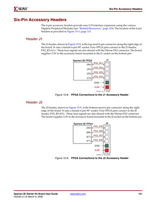
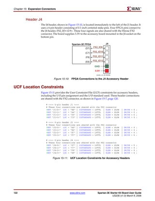
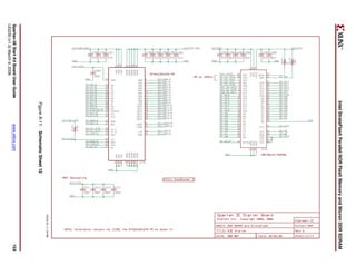
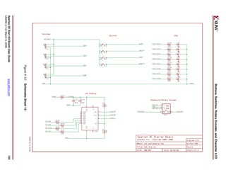
The document provides a user guide for the Spartan-3E Starter Kit Board, covering its key components and features. The board includes switches, buttons, LEDs, and multiple clock sources. It is intended for learning Xilinx FPGA and software basics as well as for more advanced development. The guide describes the purpose and operation of each component and how to interface with them in a design.
![R
Connecting Analog Inputs . . . . . . . . . . . . . . . . . . . . . . . . . . . . . . . . . . . . . . . . . . . . . . . . . . 79
Related Resources . . . . . . . . . . . . . . . . . . . . . . . . . . . . . . . . . . . . . . . . . . . . . . . . . . . . . . . . . . . 79
Chapter 11: Intel StrataFlash Parallel NOR Flash PROM
StrataFlash Connections . . . . . . . . . . . . . . . . . . . . . . . . . . . . . . . . . . . . . . . . . . . . . . . . . . . . . 82
Shared Connections . . . . . . . . . . . . . . . . . . . . . . . . . . . . . . . . . . . . . . . . . . . . . . . . . . . . . . . . . 85
Character LCD . . . . . . . . . . . . . . . . . . . . . . . . . . . . . . . . . . . . . . . . . . . . . . . . . . . . . . . . . . . 85
Xilinx XC2C64A CPLD . . . . . . . . . . . . . . . . . . . . . . . . . . . . . . . . . . . . . . . . . . . . . . . . . . . . 85
SPI Data Line . . . . . . . . . . . . . . . . . . . . . . . . . . . . . . . . . . . . . . . . . . . . . . . . . . . . . . . . . . . . 85
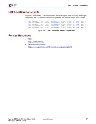
UCF Location Constraints . . . . . . . . . . . . . . . . . . . . . . . . . . . . . . . . . . . . . . . . . . . . . . . . . . . 86
Address . . . . . . . . . . . . . . . . . . . . . . . . . . . . . . . . . . . . . . . . . . . . . . . . . . . . . . . . . . . . . . . . . 86
Data . . . . . . . . . . . . . . . . . . . . . . . . . . . . . . . . . . . . . . . . . . . . . . . . . . . . . . . . . . . . . . . . . . . . 86
Control . . . . . . . . . . . . . . . . . . . . . . . . . . . . . . . . . . . . . . . . . . . . . . . . . . . . . . . . . . . . . . . . . . 87
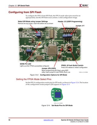
Setting the FPGA Mode Select Pins . . . . . . . . . . . . . . . . . . . . . . . . . . . . . . . . . . . . . . . . . . 87
Related Resources . . . . . . . . . . . . . . . . . . . . . . . . . . . . . . . . . . . . . . . . . . . . . . . . . . . . . . . . . . . 87
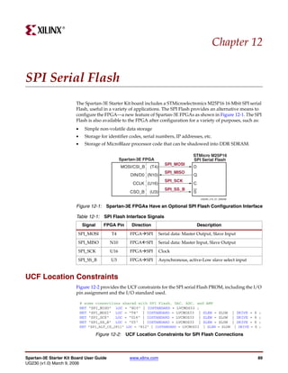
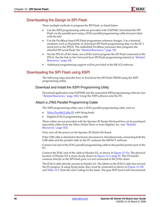
Chapter 12: SPI Serial Flash
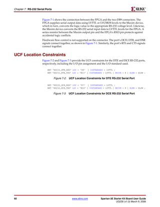
UCF Location Constraints . . . . . . . . . . . . . . . . . . . . . . . . . . . . . . . . . . . . . . . . . . . . . . . . . . . 89
Configuring from SPI Flash . . . . . . . . . . . . . . . . . . . . . . . . . . . . . . . . . . . . . . . . . . . . . . . . . 90
Setting the FPGA Mode Select Pins . . . . . . . . . . . . . . . . . . . . . . . . . . . . . . . . . . . . . . . . . . 90
Creating an SPI Serial Flash PROM File . . . . . . . . . . . . . . . . . . . . . . . . . . . . . . . . . . . . . . 91
Setting the Configuration Clock Rate . . . . . . . . . . . . . . . . . . . . . . . . . . . . . . . . . . . . . . . 91
Formatting an SPI Flash PROM File . . . . . . . . . . . . . . . . . . . . . . . . . . . . . . . . . . . . . . . . 92
Downloading the Design to SPI Flash . . . . . . . . . . . . . . . . . . . . . . . . . . . . . . . . . . . . . . . 96
Downloading the SPI Flash using XSPI . . . . . . . . . . . . . . . . . . . . . . . . . . . . . . . . . . . . . . 96
Download and Install the XSPI Programming Utility. . . . . . . . . . . . . . . . . . . . . . . . . . . 96
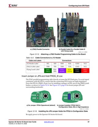
Attach a JTAG Parallel Programming Cable . . . . . . . . . . . . . . . . . . . . . . . . . . . . . . . . . . 96
Insert Jumper on JP8 and Hold PROG_B Low . . . . . . . . . . . . . . . . . . . . . . . . . . . . . . . . 97
Programming the SPI Flash with the XSPI Software . . . . . . . . . . . . . . . . . . . . . . . . . . . . 98
Additional Design Details . . . . . . . . . . . . . . . . . . . . . . . . . . . . . . . . . . . . . . . . . . . . . . . . . . . 99
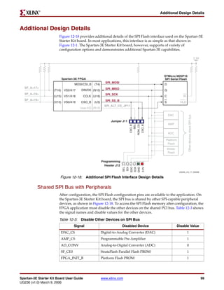
Shared SPI Bus with Peripherals . . . . . . . . . . . . . . . . . . . . . . . . . . . . . . . . . . . . . . . . . . . . 99
Other SPI Flash Control Signals . . . . . . . . . . . . . . . . . . . . . . . . . . . . . . . . . . . . . . . . . . . . 100
Variant Select Pins, VS[2:0] . . . . . . . . . . . . . . . . . . . . . . . . . . . . . . . . . . . . . . . . . . . . . . . . 100
Jumper Block J11 . . . . . . . . . . . . . . . . . . . . . . . . . . . . . . . . . . . . . . . . . . . . . . . . . . . . . . . . 100
Programming Header J12 . . . . . . . . . . . . . . . . . . . . . . . . . . . . . . . . . . . . . . . . . . . . . . . . . 100
Multi-Package Layout . . . . . . . . . . . . . . . . . . . . . . . . . . . . . . . . . . . . . . . . . . . . . . . . . . . . 100
Related Resources . . . . . . . . . . . . . . . . . . . . . . . . . . . . . . . . . . . . . . . . . . . . . . . . . . . . . . . . . . 102
Chapter 13: DDR SDRAM
DDR SDRAM Connections . . . . . . . . . . . . . . . . . . . . . . . . . . . . . . . . . . . . . . . . . . . . . . . . 104
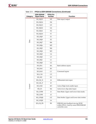
UCF Location Constraints . . . . . . . . . . . . . . . . . . . . . . . . . . . . . . . . . . . . . . . . . . . . . . . . . . 106
Address . . . . . . . . . . . . . . . . . . . . . . . . . . . . . . . . . . . . . . . . . . . . . . . . . . . . . . . . . . . . . . . . 106
Data . . . . . . . . . . . . . . . . . . . . . . . . . . . . . . . . . . . . . . . . . . . . . . . . . . . . . . . . . . . . . . . . . . . 106
Control . . . . . . . . . . . . . . . . . . . . . . . . . . . . . . . . . . . . . . . . . . . . . . . . . . . . . . . . . . . . . . . . . 107
Reserve FPGA VREF Pins . . . . . . . . . . . . . . . . . . . . . . . . . . . . . . . . . . . . . . . . . . . . . . . . . 107
Related Resources . . . . . . . . . . . . . . . . . . . . . . . . . . . . . . . . . . . . . . . . . . . . . . . . . . . . . . . . . . 107
6 www.xilinx.com Spartan-3E Starter Kit Board User Guide
UG230 (v1.0) March 9, 2006](https://image.slidesharecdn.com/spartan3e-120304054652-phpapp01/85/Spartan-3e-6-320.jpg)


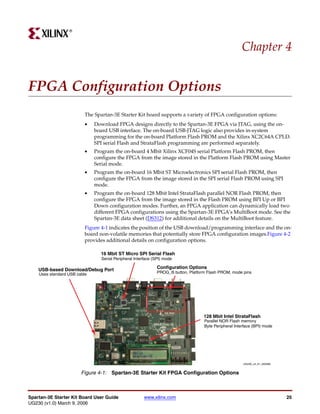
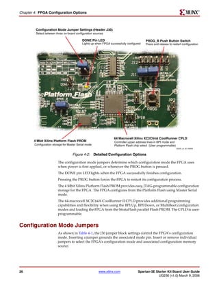
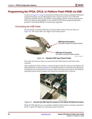
![R
PROG Push Button
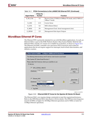
Table 4-1: Spartan-3E Configuration Mode Jumper Settings (Header J30 in
Figure 4-2)
Configuration Mode Pins
Mode M2:M1:M0 FPGA Configuration Image Source Jumper Settings
Master Serial 0:0:0 Platform Flash PROM
M0
M1
M2
J30
SPI 1:1:0 SPI Serial Flash PROM starting at
(see address 0 M0
Chapter 12, M1
“SPI Serial M2
Flash”)
J30
BPI Up 0:1:0 StrataFlash parallel Flash PROM,
(see starting at address 0 and M0
Chapter 11, incrementing through address M1
“Intel space. The CPLD controls address M2
StrataFlash lines A[24:20] during BPI
configuration. J30
Parallel NOR
Flash
PROM”)
BPI Down 0:1:1 StrataFlash parallel Flash PROM,
(see starting at address 0x1FF_FFFF and M0
Chapter 11, decrementing through address M1
“Intel space. The CPLD controls address M2
StrataFlash lines A[24:20] during BPI
configuration. J30
Parallel NOR
Flash
PROM”)
JTAG 0:1:0 Downloaded from host via USB-
JTAG port M0
M1
M2
J30
PROG Push Button
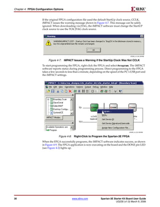
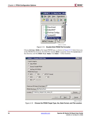
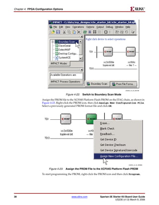
The PROG push button, shown in Figure 4-2, page 26, forces the FPGA to reconfigure from
the selected configuration memory source. Press and release this button to restart the
FPGA configuration process at any time.
DONE Pin LED
The DONE pin LED, shown in Figure 4-2, page 26, lights whenever the FPGA is
successfully configured. If this LED is not lit, then the FPGA is not configured.
Spartan-3E Starter Kit Board User Guide www.xilinx.com 27
UG230 (v1.0) March 9, 2006](https://image.slidesharecdn.com/spartan3e-120304054652-phpapp01/85/Spartan-3e-27-320.jpg)
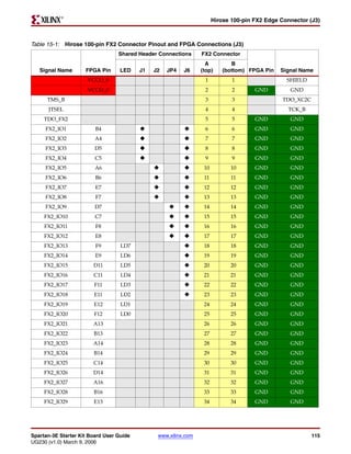
![R
Chapter 5
Character LCD Screen
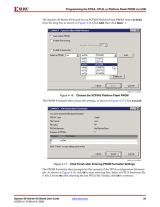
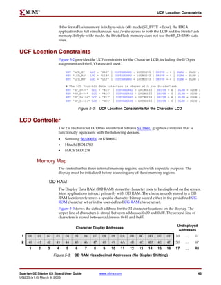
Overview
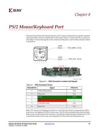
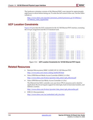
The Spartan-3E Starter Kit board prominently features a 2-line by 16-character liquid
crystal display (LCD). The FPGA controls the LCD via the 4-bit data interface shown in
Figure 5-1. Although the LCD supports an 8-bit data interface, the Starter Kit board uses a
4-bit data interface to remain compatible with other Xilinx development boards and to
minimize total pin count.
Spartan-3E FPGA Character LCD
SF_D<11> 390Ω
(M15) DB7
SF_D<10> 390Ω
(P17) DB6 Four-bit data
SF_D<9> 390Ω interface
(R16) DB5
SF_D<8> 390Ω
(R15) DB4
DB[3:0] Unused
LCD_E
(M18) E
LCD_RS
(L18) RS
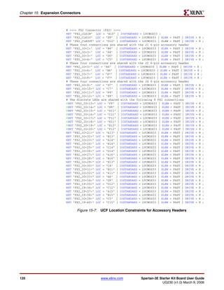
LCD_RW
(L17) R/W
Intel StrataFlash
D[11:8]
‘1’
SF_CE0 CE0
UG230_c5_01_022006
Figure 5-1: Character LCD Interface
Once mastered, the LCD is a practical way to display a variety of information using
standard ASCII and custom characters. However, these displays are not fast. Scrolling the
display at half-second intervals tests the practical limit for clarity. Compared with the
50 MHz clock available on the board, the display is slow. A PicoBlaze processor efficiently
controls display timing plus the actual content of the display.
Spartan-3E Starter Kit Board User Guide www.xilinx.com 41
UG230 (v1.0) March 9, 2006](https://image.slidesharecdn.com/spartan3e-120304054652-phpapp01/85/Spartan-3e-41-320.jpg)
![R
Chapter 5: Character LCD Screen
Physically, there are 80 total character locations in DD RAM with 40 characters available
per line. Locations 0x10 through 0x27 and 0x50 through 0x67 can be used to store other
non-display data. Alternatively, these locations can also store characters that can only
displayed using controller’s display shifting functions.
The Set DD RAM Address command initializes the address counter before reading or
writing to DD RAM. Write DD RAM data using the Write Data to CG RAM or DD RAM
command, and read DD RAM using the Read Data from CG RAM or DD RAM command.
The DD RAM address counter either remains constant after read or write operations, or
auto-increments or auto-decrements by one location, as defined by the I/D set by the Entry
Mode Set command.
CG ROM
The Character Generator ROM (CG ROM) contains the font bitmap for each of the
predefined characters that the LCD screen can display, shown in Figure 5-4. The character
code stored in DD RAM for each character location subsequently references a position with
the CG ROM. For example, a hexadecimal character code of 0x53 stored in a DD RAM
location displays the character ‘S’. The upper nibble of 0x53 equates to DB[7:4]=”0101”
binary and the lower nibble equates to DB[3:0] = “0011” binary. As shown in Figure 5-4, the
character ‘S’ appears on the screen.
English/Roman characters are stored in CG ROM at their equivalent ASCII code address.
44 www.xilinx.com Spartan-3E Starter Kit Board User Guide
UG230 (v1.0) March 9, 2006](https://image.slidesharecdn.com/spartan3e-120304054652-phpapp01/85/Spartan-3e-44-320.jpg)
![R
Chapter 5: Character LCD Screen
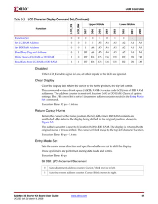
After the write operation, the address is automatically incremented or decremented by 1
according to the Entry Mode Set command. The entry mode also determines display shift.
Execution Time: 40 μs
Read Data from CG RAM or DD RAM
Read data from DD RAM if the command follows a previous Set DD RAM Address
command, or read data from CG RAM if the command follows a previous Set CG RAM
Address command.
After the read operation, the address is automatically incremented or decremented by 1
according to the Entry Mode Set command. However, a display shift is not executed
during read operations.
Execution Time: 40 μs
Operation
Four-Bit Data Interface
The board uses a 4-bit data interface to the character LCD.
Figure 5-6 illustrates a write operation to the LCD, showing the minimum times allowed
for setup, hold, and enable pulse length relative to the 50 MHz clock (20 ns period)
provided on the board.
CLOCK
LCD_RS 0 = Command, 1 = Data
SF_D[11:8] Valid Data
LCD_RW
LCD_E
230 ns
40 ns 10 ns
Upper Lower
4 bits 4 bits
LCD_RS
SF_D[11:8]
LCD_RW
LCD_E
1 μs 40 μs
UG230_c5_03_022006
Figure 5-6: Character LCD Interface Timing
50 www.xilinx.com Spartan-3E Starter Kit Board User Guide
UG230 (v1.0) March 9, 2006](https://image.slidesharecdn.com/spartan3e-120304054652-phpapp01/85/Spartan-3e-50-320.jpg)
![R
Keyboard
ESC F1 F2 F3 F4 F5 F6 F7 F8 F9 F10 F11 F12
76 05 06 04 0C 03 0B 83 0A 01 09 78 07 E0 75
`~ 1! 2@ 3# 4$ 5% 6^ 7& 8* 9( 0) -_ =+ Back Space
0E 16 1E 26 25 2E 36 3D 3E 46 45 4E 55 66 E0 74
TA B Q W E R T Y U I O P [{ ]} |
0D 15 1D 24 2D 2C 35 3C 43 44 4D 54 5B 5D E0 6B
Caps Lock A S D F G H J K L ;: '" Enter
58 1C 1B 23 2B 34 33 3B 42 4B 4C 52 5A
E0 72
Shift Z X C V B N M ,< >. /? Shift
12 1Z 22 21 2A 32 31 3A 41 49 4A 59
Ctrl Alt Space Alt Ctrl
14 11 29 E0 11 E0 14
UG230_c8_03_021806
Figure 8-3: PS/2 Keyboard Scan Codes
The host can also send commands and data to the keyboard. Table 8-3 provides a short list
of some often-used commands.
Table 8-3: Common PS/2 Keyboard Commands
Command Description
ED Turn on/off Num Lock, Caps Lock, and Scroll Lock LEDs. The keyboard acknowledges receipt of an
“ED” command by replying with an “FA”, after which the host sends another byte to set LED status. The
bit positions for the keyboard LEDs are shown below. Write a ‘1’ to the specific bit to illuminate the
associated keyboard LED.
7 6 5 4 3 2 1 0
Ignored Caps Lock Num Lock Scroll Lock
EE Echo. Upon receiving an echo command, the keyboard replies with the same scan code “EE”.
F3 Set scan code repeat rate. The keyboard acknowledges receipt of an “F3” by returning an “FA”, after
which the host sends a second byte to set the repeat rate.
FE Resend. Upon receiving a resend command, the keyboard resends the last scan code sent.
FF Reset. Resets the keyboard.
The keyboard sends commands or data to the host only when both the data and clock lines
are High, the Idle state.
Because the host is the bus master, the keyboard checks whether the host is sending data
before driving the bus. The clock line can be used as a clear to send signal. If the host pulls
the clock line Low, the keyboard must not send any data until the clock is released.
The keyboard sends data to the host in 11-bit words that contain a ‘0’ start bit, followed by
eight bits of scan code (LSB first), followed by an odd parity bit and terminated with a ‘1’
stop bit. When the keyboard sends data, it generates 11 clock transitions at around 20 to
30 kHz, and data is valid on the falling edge of the clock as shown in Figure 8-2.
Spartan-3E Starter Kit Board User Guide www.xilinx.com 63
UG230 (v1.0) March 9, 2006](https://image.slidesharecdn.com/spartan3e-120304054652-phpapp01/85/Spartan-3e-63-320.jpg)
![R
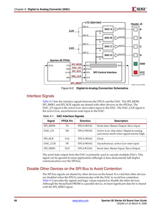
Chapter 9: Digital to Analog Converter (DAC)
SPI_MISO
0 Slave: LTC2624 DAC 31
SPI_MOSI
x x x x 0 1 2 3 4 5 6 7 8 9 10 11 a0 a1 a2 a3 c0 c1 c2 c3 x x x x x x x x
DAC_CS lsb msb
Master
Spartan-3E SPI_SCK
Don’t Care Don’t Care
FPGA 12-bit Unsigned
DATA
COMMAND
a3 a2 a1 a0 ADDRESS
0 0 0 0 DAC A
0 0 0 1 DAC B
0 0 1 0 DAC C
0 0 1 1 DAC D
1 1 1 1 All UG230_c9_04_021806
Figure 9-4: SPI Communications Protocol to LTC2624 DAC
The FPGA first sends eight dummy or “don’t care” bits, followed by a 4-bit command. The
most commonly used command with the board is COMMAND[3:0] = “0011”, which
immediately updates the selected DAC output with the specified data value. Following the
command, the FPGA selects one or all the DAC output channels via a 4-bit address field.
Following the address field, the FPGA sends a 12-bit unsigned data value that the DAC
converts to an analog value on the selected output(s). Finally, four additional dummy or
don’t care bits pad the 32-bit command word.
Specifying the DAC Output Voltage
As shown in Figure 9-2, each DAC output level is the analog equivalent of a 12-bit
unsigned digital value, D[11:0], written by the FPGA to the DAC via the SPI interface.
The voltage on a specific output is generally described in Equation 9-1. The reference
voltage, VREFERENCE, is different between the four DAC outputs. Channels A and B use a
3.3V reference voltage and Channels C and D use a 2.5V reference. The reference voltages
themselves have a ±5% tolerance, so there will be slight corresponding variances in the
output voltage.
D [ 11:0 ]
V OUT = -------------------- × V REFERENCE
- Equation 9-1
,
4096
DAC Outputs A and B
Equation 9-2 provides the output voltage equation for DAC outputs A and B. The
reference voltage associated with DAC outputs A and B is 3.3V ± 5%.
D [ 11:0 ]
V OUTA = -------------------- × ( 3.3V ± 5% )
- Equation 9-2
,
4096
DAC Outputs C and D
Equation 9-3 provides the output voltage equation for DAC outputs A and B. The
reference voltage associated with DAC outputs A and B is 2.5V ± 5%.
D [ 11:0 ]
V OUTC = -------------------- × ( 2.5V ± 5% )
- Equation 9-3
,
4096
70 www.xilinx.com Spartan-3E Starter Kit Board User Guide
UG230 (v1.0) March 9, 2006](https://image.slidesharecdn.com/spartan3e-120304054652-phpapp01/85/Spartan-3e-70-320.jpg)
![R
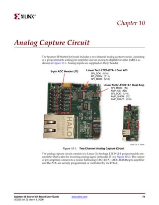
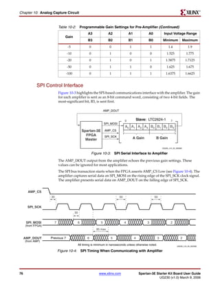
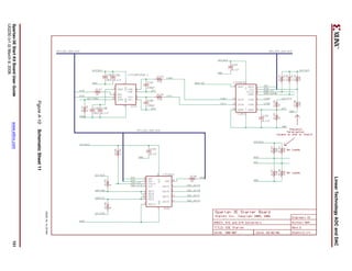
Chapter 10: Analog Capture Circuit
Header J7
REFAB
(3.3V)
REFCD
(2.5V)
LTC 6912-1 AMP LTC 1407A-1 ADC
VINA
A A/D
Channel 0
14
VINB
B A/D
Channel 1
GND
VCC
(3.3V)
14
REF = 1.65V
Spartan-3E FPGA
SPI_MOSI
(N10) (T4) DIN 0 1 2 3 0 1 2 3 DOUT 0 ... 13 0 ... 13 SDO
(E18) (N7) AMP_CS CS/LD A GAIN B GAIN CHANNEL 1 CHANNEL 0
(U16) SPI_SCK SCK SPI Control Interface SCK SPI Control Interface
AMP_SHDN
(P7) SHDN CONV
AD_CONV
(P11)
AMP_DOUT
SPI_MISO
UG230_c10_02_022306
Figure 10-2: Detailed View of Analog Capture Circuit
Digital Outputs from Analog Inputs
The analog capture circuit converts the analog voltage on VINA or VINB and converts it to
a 14-bit digital representation, D[13:0], as expressed by Equation 10-1.
( V IN – 1.65V )
D [ 13:0 ] = GAIN × ----------------------------------- × 8192
- Equation 10-1
1.25V
The GAIN is the current setting loaded into the programmable pre-amplifier. The various
allowable settings for GAIN and allowable voltages applied to the VINA and VINB inputs
appear in Table 10-2.
The reference voltage for the amplifier and the ADC is 1.65V, generated via a voltage
divider shown in Figure 10-2. Consequently, 1.65V is subtracted from the input voltage on
VINA or VINB.
The maximum range of the ADC is ±1.25V, centered around the reference voltage, 1.65V.
Hence, 1.25V appears in the denominator to scale the analog input accordingly.
74 www.xilinx.com Spartan-3E Starter Kit Board User Guide
UG230 (v1.0) March 9, 2006](https://image.slidesharecdn.com/spartan3e-120304054652-phpapp01/85/Spartan-3e-74-320.jpg)
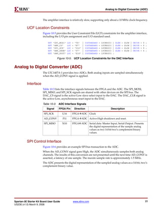
![R
Chapter 11
Intel StrataFlash Parallel NOR Flash
PROM
As shown in Figure 11-1, the Spartan-3E Starter Kit boards includes a 128 Mbit (16 Mbyte)
Intel StrataFlash parallel NOR Flash PROM. As indicated, some of the StrataFlash
connections are shared with other components on the board.
Intel StrataFlash
SPI Serial Flash
CE2
Spartan-3E FPGA
CE1 Q
SF_CE0
LDC0 CE0
SF_OE
LDC1 OE# ADC
SF_WE
HDC WE#
SF_BYTE SDO
LDC2 BYTE#
SF_STS
User I/O STS
SF_D<15:12> DAC
User I/O D[15:12]
SF_D<11:8>
User I/O D[11:8] SDO
SF_D<7:1>
D[7:1] D[7:1]
SPI_MISO
D[0] D[0]
SF_A<24:20> Platform Flash
User I/O A[24:20]
SF_A<19:0>
A[19:0] A[19:0] D0
A[23:20]
CoolRunner-II CPLD Character LCD
[7:4]
DB[7:4]
UG230_c11_01_030206
Figure 11-1: Connections to Intel StrataFlash Flash Memory
The StrataFlash PROM provides various functions:
• Stores a single FPGA configuration in the StrataFlash device.
• Stores two different FPGA configurations in the StrataFlash device and dynamically
switch between the two using the Spartan-3E FPGA’s MultiBoot feature.
• Stores and executes MicroBlaze processor code directly from the StrataFlash device.
Spartan-3E Starter Kit Board User Guide www.xilinx.com 81
UG230 (v1.0) March 9, 2006](https://image.slidesharecdn.com/spartan3e-120304054652-phpapp01/85/Spartan-3e-81-320.jpg)
![R
Chapter 11: Intel StrataFlash Parallel NOR Flash PROM
• Stores MicroBlaze processor code in the StrataFlash device and shadows the code into
the DDR memory before executing the code.
• Stores non-volatile data from the FPGA.
StrataFlash Connections
Table 11-1 shows the connections between the FPGA and the StrataFlash device.
Although the XC3S500E FPGA only requires just slightly over 2 Mbits per configuration
image, the FPGA-to-StrataFlash interface on the board support up to a 256 Mbit
StrataFlash. The Spartan-3E Starter Kit board ships with a 128 Mbit device. Address line
SF_A24 is not used.
In general, the StrataFlash device connects to the XC3S500E to support Byte Peripheral
Interface (BPI) configuration. The upper four address bits from the FPGA, A[23:19] do not
connect directly to the StrataFlash device. Instead, the XC2C64 CPLD controls the pins
during configuration. As described in Table 11-1 and Shared Connections, some of the
StrataFlash connections are shared with other components on the board.
82 www.xilinx.com Spartan-3E Starter Kit Board User Guide
UG230 (v1.0) March 9, 2006](https://image.slidesharecdn.com/spartan3e-120304054652-phpapp01/85/Spartan-3e-82-320.jpg)
![R
StrataFlash Connections
Table 11-1: FPGA-to-StrataFlash Connections
StrataFlash FPGA Pin
Category Signal Name Number Function
SF_A24 A11 Shared with XC2C64A CPLD. The CPLD
actively drives these pins during FPGA
SF_A23 N11
configuration, as described in Chapter 16,
SF_A22 V12 “XC2C64A CoolRunner-II CPLD”. Also
connects to FPGA user-I/O pins. SF_A24 is the
SF_A21 V13
same as FX2 connector signal FX2_IO<32>.
SF_A20 T12
SF_A19 V15 Connects to FPGA pins A[19:0] to support the
BPI configuration.
SF_A18 U15
SF_A17 T16
SF_A16 U18
SF_A15 T17
SF_A14 R18
SF_A13 T18
Address
SF_A12 L16
SF_A11 L15
SF_A10 K13
SF_A9 K12
SF_A8 K15
SF_A7 K14
SF_A6 J17
SF_A5 J16
SF_A4 J15
SF_A3 J14
SF_A2 J12
SF_A1 J13
SF_A0 H17
Spartan-3E Starter Kit Board User Guide www.xilinx.com 83
UG230 (v1.0) March 9, 2006](https://image.slidesharecdn.com/spartan3e-120304054652-phpapp01/85/Spartan-3e-83-320.jpg)
![R
Chapter 11: Intel StrataFlash Parallel NOR Flash PROM
Table 11-1: FPGA-to-StrataFlash Connections
StrataFlash FPGA Pin
Category Signal Name Number Function
SF_D15 T8 Upper 8 bits of a 16-bit
halfword when
SF_D14 R8
StrataFlash is -
SF_D13 P6 configured for x16
data
SF_D12 M16
(SF_BYTE=High).
SF_D11 M15 Connects to FPGA Signals SF_D<11:8>
user I/O. connect to character
SF_D10 P17
LCD pins DB[7:4].
SF_D9 R16
SF_D8 R15
SF_D7 N9 Upper 7 bits of a data byte or lower 8 bits of a
Data
16-bit halfword. Connects to FPGA pins D[7:1]
SF_D6 M9
to support the BPI configuration.
SF_D5 R9
SF_D4 U9
SF_D3 V9
SF_D2 R10
SF_D1 P10
SPI_MISO N10 Bit 0 of data byte and 16-bit halfword.
Connects to FPGA pin D0/DIN to support the
BPI configuration. Shared with other SPI
peripherals and Platform Flash PROM.
SF_CE0 D16 StrataFlash Chip Enable. Connects to FPGA
pin LDC0 to support the BPI configuration.
SF_WE D17 StrataFlash Write Enable. Connects to FPGA
pin HDC to support the BPI configuration.
SF_OE C18 StrataFlash Chip Enable. Connects to FPGA
Control
pin LDC1 to support the BPI configuration.
SF_BYTE C17 StrataFlash Byte Enable. Connects to FPGA pin
LDC2 to support the BPI configuration.
0: x8 data
1: x16 data
SF_STS B18 StrataFlash Status signal. Connects to FPGA
user-I/O pin.
84 www.xilinx.com Spartan-3E Starter Kit Board User Guide
UG230 (v1.0) March 9, 2006](https://image.slidesharecdn.com/spartan3e-120304054652-phpapp01/85/Spartan-3e-84-320.jpg)
![R
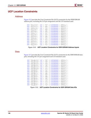
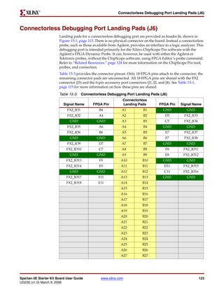
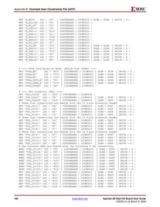
Setting the FPGA Mode Select Pins
Control
Figure 11-4 provides the UCF constraints for the StrataFlash control pins, including the
I/O pin assignment and the I/O standard used.
NET "SF_BYTE" LOC = "C17" | IOSTANDARD = LVCMOS33 | DRIVE = 4 | SLEW = SLOW ;
NET "SF_CE0" LOC = "D16" | IOSTANDARD = LVCMOS33 | DRIVE = 4 | SLEW = SLOW ;
NET "SF_OE" LOC = "C18" | IOSTANDARD = LVCMOS33 | DRIVE = 4 | SLEW = SLOW ;
NET "SF_STS" LOC = "B18" | IOSTANDARD = LVCMOS33 | DRIVE = 4 | SLEW = SLOW ;
NET "SF_WE" LOC = "D17" | IOSTANDARD = LVCMOS33 | DRIVE = 4 | SLEW = SLOW ;
Figure 11-4: UCF Location Constraints for StrataFlash Control Pins
Setting the FPGA Mode Select Pins
Set the FPGA configuration mode pins for either BPI Up or BPI down mode, as shown in
Table 11-4. See
Table 11-4: Selecting BPI-Up or BPI-Down Configuration Modes (Header J30 in
Figure 4-2)
Configuration Mode Pins FPGA Configuration Image in
Mode M2:M1:M0 StrataFlash Jumper Settings
BPI Up 0:1:0 FPGA starts at address 0 and
increments through address space. M0
The CPLD controls address lines M1
A[24:20] during BPI configuration. M2
J30
BPI Down 0:1:1 FPGA starts at address 0xFF_FFFF
and decrements through address M0
space. The CPLD controls address M1
lines A[24:20] during BPI M2
configuration.
J30
Related Resources
• Intel J3 StrataFlash Data Sheet
http://www.intel.com/design/flcomp/products/j3/techdocs.htm#datasheets
• Application Note 827, Intel StrataFlash® Memory (J3) to Xilinx Spartan-3E FPGA
Design Guide
http://www.intel.com/design/flcomp/applnots/307257.htm
Spartan-3E Starter Kit Board User Guide www.xilinx.com 87
UG230 (v1.0) March 9, 2006](https://image.slidesharecdn.com/spartan3e-120304054652-phpapp01/85/Spartan-3e-87-320.jpg)
![R
Chapter 12: SPI Serial Flash
Programming the SPI Flash with the XSPI Software
Open a command prompt or DOS box and change to the XSPI installation directory.
The XSPI installation software also includes a short user guide, in addition to XAPP445.
Type xspi at the prompt to view quick help.
Type the following command at the prompt to program the SPI Flash using the SPI-
formatted Flash file generated earlier. This verifies that the SPI Flash is indeed an M25P16
SPI Flash and then erases, programs, and finally verifies the Flash.
C:xspi>xspi -spi_dev m25p16 -spi_epv -mcs -i MySPIFlash.mcs -o output.txt
A disclaimer notice appears on the screen. Press the Enter key to continue. The entire
programming process takes slightly longer than a minute, as shown in Figure 12-17.
-==< Press ENTER to accept notice and continue >==-
Start : Mon Feb 27 13:37:07 2006
==> Checking SPI device [STMicro_M25P16_ver_00100] ID code(s)
- density = [2097152] bytes
= [16777216] bits
- mfg_code = [0x20]
- memory_type = [0x20]
- density_code = [0x15]
+-----------------------------------------+
| Device ID code(s) check ====> [ OK ] |
+-----------------------------------------+
=> Operation: Erase
=> Operation: Program and Verify using file [MySPIFlash.mcs]
Programmed [283776] of [283776] bytes (w/ polling)
Verified [283776] of [283776] bytes (0 errors)
--> Total byte mismatches [0] (see [temp.txt])
Finish : Mon Feb 27 13:38:22 2006
Elapsed clock time (00:01:15) = 75 seconds
Figure 12-17: Programming the M25P16 SPI Flash with the XSPI Programming
Utility
After programming the SPI Flash, remove jumper JP8, as shown in Figure 12-16a. If
properly programmed, the FPGA then configures itself from the SPI Flash PROM and the
DONE LED lights. The DONE LED is shown in Figure 12-3.
98 www.xilinx.com Spartan-3E Starter Kit Board User Guide
UG230 (v1.0) March 9, 2006](https://image.slidesharecdn.com/spartan3e-120304054652-phpapp01/85/Spartan-3e-98-320.jpg)
![R
Chapter 12: SPI Serial Flash
Other SPI Flash Control Signals
The M25P16 SPI Flash has two additional control inputs. The active-Low write protect
input (W) and the active-Low bus hold input (HLD) are unused and pulled High via an
external pull-up resistor.
Variant Select Pins, VS[2:0]
When in SPI configuration mode, the FPGA samples the value on three pins, labeled
VS[2:0], to determine which SPI read command to issue to the SPI Flash. For the M25P16
Flash, VS[2:0]=<1:1:1> issues the correct command sequence. The VS[2:0] pins are pulled
High externally via pull-up resistors to 3.3V. The VS[2:0] pins are also parallel NOR Flash
address lines A[19:17] in the FPGA’s BPI configuration mode and these signals also
connect to the StrataFlash parallel Flash PROM. After SPI configuration, the VS[2:0] pins
become user-programmable I/O pins, allowing full access to the StrataFlash PROM,
despite that the FPGA configured from SPI Flash.
Jumper Block J11
In SPI configuration mode, the FPGA selects the attached SPI Flash by asserting the CSO_B
pin Low. On the Spartan-3E Starter Kit board, the CSO_B pin drives into the jumper J11
block. This jumper block provides the option to move the on-board SPI Flash to a different
select line (SPI_ALT_CS_JP11). This way, a different SPI Flash device can be tested by
changing the JP11 jumper settings and connecting the alternate SPI Flash on Header JP12.
By default, both jumpers are inserted on jumper block header J11.
Programming Header J12
As shown in Figure 12-15, page 97, Header J12 accepts a JTAG parallel programming cable
to program the on-board SPI Flash.
Multi-Package Layout
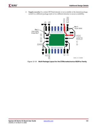
STMicroelectronics was rather clever when they defined the package layout for the
M25Pxx SPI serial Flash family. The Spartan-3E Starter Kit board supports all three of the
package types used for the 16 Mbit device, as shown in Figure 12-19. By default, the board
ships with the 8-lead, 8x6 mm MLP package. The multi-package layout also supports the 8-
pin SOIC package and the 16-pin SOIC package. Pin 1 for the 8-pin SOIC and MLP
packages is located in the top-left corner. However, pin 1 for the 16-pin SOIC package is
located in the top-right corner, because the package is rotated 90°. The 16-pin SOIC
package also have four pins on each side that do not connect on the board. These pins must
be left floating. Why support multiple packages? In a word, flexibility. The multi-package
layout provides ...
• Density migration between smaller- and larger-density SPI Flash PROMs. Not all
SPI Flash densities are available in all packages. The SPI Flash migration strategy
follows nicely with the pinout migration provided by Xilinx FPGAs.
• Consistent configuration PROM layout when migrating between FPGA densities.
The Spartan-3E FPGA’s FG320 package footprint supports the XC3S500E, the
XC3S1200E, and the XC3S1600E FPGA devices without modification. The SPI Flash
multi-package layout allows comparable flexibility in the associated configuration
PROM. Ship the optimally-sized SPI Flash memory for the FPGA mounted on the
board.
100 www.xilinx.com Spartan-3E Starter Kit Board User Guide
UG230 (v1.0) March 9, 2006](https://image.slidesharecdn.com/spartan3e-120304054652-phpapp01/85/Spartan-3e-100-320.jpg)

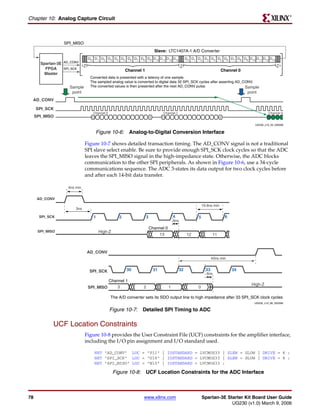
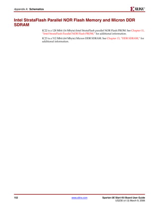
![R
Chapter 13
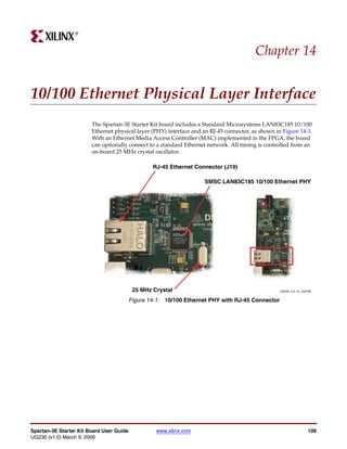
DDR SDRAM
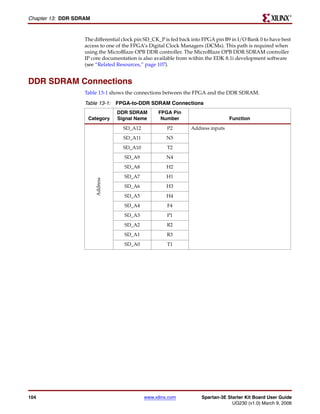
The Spartan-3E Starter Kit boards includes a 512 Mbit (32M x 16) Micron Technology DDR
SDRAM (MT46V32M16) with a 16-bit data interface, as shown in Figure 13-1. All DDR
SDRAM interface pins connect to the FPGA’s I/O Bank 3 on the FPGA. I/O Bank 3 and the
DDR SDRAM are both powered by 2.5V, generated by an LTC3412 regulator from the
board’s 5V supply input. The 1.25V reference voltage, common to the FPGA and DDR
SDRAM, is generated using a resistor voltage divider from the 2.5V rail.
5.0V
2.5V
LTC3412
1.25V
Spartan-3E FPGA Micron 512 Mb DDR SDRAM
SD_A<12:0>
See Table A[12:0]
SD_DQ<15:0>
VREF See Table DQ[15:0] VREF
SD_BA<1:0>
VCCO_3 See Table BA[1:0] VDD
SD_RAS
(C1) RAS# VDDQ
SD_CAS
(C2) CAS#
SD_WE
(D1) WE#
SD_UDM
(J1) UQM MT46V32M16
SD_LDM (32Mx16)
(J2) LQM
SD_UDQS
(G3) UDQS
SD_LDQS
(L6) LDQS
SD_CS
(K4) CS#
SD_CKE
(K3) CKE
SD_CK_N
(J4) CK#
SD_CK_P
(B9) GCLK9 (J5) CK
SD_CK_FB
UG230_c13_01_022406
Figure 13-1: FPGA Interface to Micron 512 Mbit DDR SDRAM
All DDR SDRAM interface signals are terminated.
Spartan-3E Starter Kit Board User Guide www.xilinx.com 103
UG230 (v1.0) March 9, 2006](https://image.slidesharecdn.com/spartan3e-120304054652-phpapp01/85/Spartan-3e-103-320.jpg)

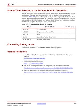
![R
Chapter 14: 10/100 Ethernet Physical Layer Interface
Ethernet PHY Connections
The FPGA connects to the LAN83C185 Ethernet PHY using a standard Media Independent
Interface (MII), as shown in Figure 14-2. A more detailed description of the interface
signals, including the FPGA pin number, appears in Table 14-1.
SMSC LAN83C185
Spartan-3E FPGA 10/100 Ethernet PHY
E_TXD<3:0>
See Table TXD[3:0]
E_TX_EN
(P15) TX_EN
E_TXD<4>
(R4) TXD4/TX_ER
E_TX_CLK
(T7) TX_CLK
E_RXD<3:0> RJ-45
See Table RXD[3:0]
Connector
E_RX_DV
(V2) RX_DV
E_RXD<4>
(U14) RXD4/RX_ER
E_RX_CLK
(V3) RX_CLK
E_CRS
(U13) CRS
25.000 MHz
E_COL
(U6) COL
E_MDC
(P9) MDC
(U5) E_MDIO MDIO
UG230_c14_02_022706
Figure 14-2: FPGA Connects to Ethernet PHY via MII
Table 14-1: FPGA Connections to the LAN83C185 Ethernet PHY
FPGA Pin
Signal Name Number Function
E_TXD<4> R6 Transmit Data to the PHY. E_TXD<4> is also the MII
Transmit Error.
E_TXD<3> T5
E_TXD<2> R5
E_TXD<1> T15
E_TXD<0> R11
E_TX_EN P15 Transmit Enable.
E_TX_CLK T7 Transmit Clock. 25 MHz in 100Base-TX mode, and 2.5 MHz
in 10Base-T mode.
E_RXD<4> U14 Receive Data from PHY.
E_RXD<3> V14
E_RXD<2> U11
E_RXD<1> T11
E_RXD<0> V8
E_RX_DV V2 Receive Data Valid.
110 www.xilinx.com Spartan-3E Starter Kit Board User Guide
UG230 (v1.0) March 9, 2006](https://image.slidesharecdn.com/spartan3e-120304054652-phpapp01/85/Spartan-3e-110-320.jpg)
![R
Chapter 16
XC2C64A CoolRunner-II CPLD
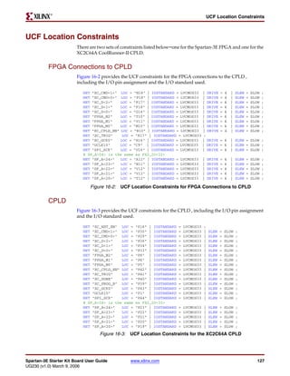
The Spartan-3E Starter Kit board includes a Xilinx XC2C64A CoolRunner-II CPLD. The
CPLD is user programmable and available for customer applications. Portions of the
CPLD are reserved to coordinate behavior between the various FPGA configuration
memories, namely the Xilinx Platform Flash PROM and the Intel StrataFlash PROM.
Consequently, the CPLD must provide the following functions in addition to the user
application.
• When the FPGA is in the Master Serial configuration mode (FPGA_M<2:0>=000),
generate an active-Low enable signal for the XCF04S Platform Flash PROM. The
Platform Flash PROM is disabled in all other configuration modes. The CPLD helps
reduce the number of jumpers on the board and simplifies the interaction of all the
possible FPGA configuration memory sources.
• When the FPGA is actively in the BPI-Up configuration mode (FPGA_M<2:0>=010,
DONE=0), set the upper five StrataFlash PROM address lines, A[24:20], to 00000
binary. When the FPGA is actively in the BPI-Down configuration mode
(FPGA_M<2:0>=011, DONE=0), set the upper five StrataFlash PROM address lines,
A[24:20], to 11111 binary. Set the upper five address lines to ZZZZZ for all non-BPI
configuration modes or whenever the FPGA’s DONE pin is High. This behavior is
identifical to the way the FPGA’s upper address lines function during BPI mode. So
why add a CPLD to mimic this behavior? A future reference design demonstrates
unique configuration capabilities. In a typical BPI-mode application, the CPLD is not
required.
Other than the required CPLD functionality, there are between 13 to 21 user-I/O pins and
58 remaining macrocells available to the user application.
Jumper JP10 (WDT_EN) defines the state on the CPLD’s XC_WDT_EN signal. By default,
this jumper is empty and the signal is pulled to a logic High.
The XC_PROG_B output from the CPLD, if used, must be configured as an open-drain out
(i.e., either actively drives Low or floats to Hi-Z, never drives High). This signal connects
directly to the FPGA’s PROG_B programming pin.
The most-siginficant StrataFlash PROM address bit, SF_A<24>, is the same as the FX2
connector signal called FX2_IO<32>. The 16 Mbyte StrataFlash PROM only physically uses
the lower 24 bits, SF_A<23:0>. The extra address bit, SF_A<24>, is provided for upward
density migration for the StrataFlash PROM.
Spartan-3E Starter Kit Board User Guide www.xilinx.com 125
UG230 (v1.0) March 9, 2006](https://image.slidesharecdn.com/spartan3e-120304054652-phpapp01/85/Spartan-3e-125-320.jpg)
![R
Chapter 16: XC2C64A CoolRunner-II CPLD
3.3V
JP10 XC2C64A VQ44
WDT_EN CoolRunner-II CPLD
XC_WDT_EN
(P16)
Spartan-3E FPGA
XC_CMD<1>
(N18) (P30)
XC_CMD<0>
(P18) (P29)
Required for Master Serial Mode
XC_D<2> Enable Platform Flash PROM when
(F17) (P36)
M[2:0]=000
XC_D<1>
(F18) (P34) XCF04S
XC_D<0> Platform Flash PROM
(G16) (P33)
FPGA_M2
(T10) (P8)
FPGA_M1 XC_PF_CE
(V11) (P6) (P2) CE
FPGA_M0
(M10) (P5)
XC_CPLD_EN
(D10) (P42)
XC_TRIG
(R17) (P41)
XC_DONE
DONE (P40)
XC_PROG_B
PROG_B (P39)
XC_GCK0
(H16) (P43)
GCLK10
(C9) (P1)
During Configuration:
SPI_SCK BPI Up: A[24:20]=00000
(U16) (FX2_IO<32>)
(P44)
BPI Down: A[24:20]=11111
SF_A<24> After Configuration or Other Modes:
(A11) (P23)
Upper Ad dress
Control During
A[24:20]=ZZZZ
Con figuration
SF_A<23>
(N11) (P22)
SF_A<22>
(V12) (P21)
Intel StrataFlash
SF_A<21>
(V13) (P20)
SF_A<20>
(T12) (P19)
A[23:20] A[24:20]
SF_A<19:0>
A[19:0] A[19:0]
A[23:20] Unconnected UG230_c16_01_030906
Figure 16-1: XC2C64A CoolRunner-II CPLD Controls Master Serial and BPI Configuration Modes
126 www.xilinx.com Spartan-3E Starter Kit Board User Guide
UG230 (v1.0) March 9, 2006](https://image.slidesharecdn.com/spartan3e-120304054652-phpapp01/85/Spartan-3e-126-320.jpg)


![5G Explained! A High Level Overview [Introduction]](https://cdn.slidesharecdn.com/ss_thumbnails/5gexplainedahighleveloverview-260119165306-cc137a3e-thumbnail.jpg?width=640&height=640&fit=bounds)


