SlideShare a Scribd company logo
4 bit Bidirectional Shift Register
• Bidirectional shift register allows shifting of data either to left or to the
right side.
• It can be implemented using logic gates circuitry that enables the transfer
of data from one stage to the next stage to the right or to the left, depend
on the level of control line.
• The RIGHT/LEFT is the control input signal which allows data shifting either
towards right or towards left.
• A high on this line enables the shifting of data towards right and low
enables it towards left.
• When RIGHT/LEFT is high, gates G1, G2, G3 and G4 are enabled.
• The state of Q output of each flip flop is passed through the D input of the
following flip flop.
• When the pulse arrives, the data are shifted one place to the right.
• When the RIGHT/LEFT signal is low, gates G5, G6, G7 are enabled.
• The Q output of each flip-flop is passed through the D input of the
preceding flip-flop.
10/20/2018
Prepared By, Ms. K. D. Patil, SCOE,
Kopargaon
4 Bit Bidirectional Shift Register
10/20/2018
Prepared By, Ms. K. D. Patil, SCOE,
Kopargaon
4 bit Ring Counter
10/20/2018
Prepared By, Ms. K. D. Patil, SCOE,
Kopargaon
Ring Counter
• Operation of Ring Counter
• Initially, all the flip flops in ring counter are reset to 0
by applying CLEAR signal. Before applying the clock
pulse, we apply the PRESET pulse to the flip flops which
assigns the value ‘1’ to the ring counter circuit. For
each clock signal, the data circulates among all the 4
flip flop stages of ring counter.
• This 4 staged ring counter is called Mod 4 ring counter
or 4 bit ring counter. To circulate the data correctly in
the ring counter, we must load the counter with
required values like all 0’s or all 1’s.
10/20/2018
Prepared By, Ms. K. D. Patil, SCOE,
Kopargaon
Ring Counter
• Truth table of ring counter
• When CLEAR input CLR = 0, then all flip flops are set to 1. When
CLEAR input CLR = 1, the ring counter starts its operation. For one
clock signal, the counter starts its operation. On next clock signal,
the counter again resets to 0000. Ring counter has 4 sequences:
0001, 0010, 0100, 1000, 0000.
10/20/2018
Prepared By, Ms. K. D. Patil, SCOE,
Kopargaon
Ring Counter
10/20/2018
Prepared By, Ms. K. D. Patil, SCOE,
Kopargaon
• State diagram of ring counter
• It denotes that the position of the preset digit
(in this case preset digit is 1) is changing its
position from LSB to MSB, for one clock signal.
10/20/2018
Prepared By, Ms. K. D. Patil, SCOE,
Kopargaon
Ring Counter
• Advantages
• Can be implemented using D and JK flip-flops.
• It is a self-decoding circuit. It doesn’t need a
decoder
• Disadvantages
• Only four of the 15 states are being utilized.
10/20/2018
Prepared By, Ms. K. D. Patil, SCOE,
Kopargaon
Johnson/Twisted Ring Counter
• The Johnson counter is a modification of ring counter. In this the inverted
output of the last stage flip flop is connected to the input of first flip flop.
If we use n flip flops to design the Johnson counter, it is known as 2n bit
Johnson counter or Mod 2n Johnson counter.
• This is an advantage of the Johnson counter that it requires only half
number of flip flops that of a ring counter uses, to design the same Mod.
• The main difference between the 4 bit ring counter and the Johnson
counter is that, in ring counter, we connect the output of last flip flop
directly to the input of first flip flop. But in Johnson counter, we connect
the inverted output of last stage to the first stage input.
• The Johnson counter is also known as Twisted Ring Counter, with a
feedback. In Johnson counter the input of the first flip flop is connected
from the inverted output of the last flip flop.
• The Johnson counter or switch trail ring counter is designed in such a way
that it overcomes the limitations of ring counter. Mainly it reduces the
number of flip flops required for designing the circuit.
10/20/2018
Prepared By, Ms. K. D. Patil, SCOE,
Kopargaon
10/20/2018
Prepared By, Ms. K. D. Patil, SCOE,
Kopargaon
• Operation of johnson counter
• The Johnson counter designed with D flip flop is
shown in figure. It has four stages i.e. four flip
flops connected in series type or cascaded.
Initially zero / Null is fed to the Johnson counter
and on applying the clock signal, outputs will
change to “1000”, “1100”, “1110”, “1111”, “0111”,
“0011”, “0001”, “0000” in a sequence and the
sequence will repeat for next clock signal.
• The Johnson counter produces a special pattern
by passing four 0’s and then four 1’s and thus it
produces a special pattern by counting up down.
10/20/2018
Prepared By, Ms. K. D. Patil, SCOE,
Kopargaon
Truth table of johnson counter
10/20/2018
Prepared By, Ms. K. D. Patil, SCOE,
Kopargaon
Timing Diagram of Johnson Ring
Counter
10/20/2018
Prepared By, Ms. K. D. Patil, SCOE,
Kopargaon
State Diagram
• The timing diagram of the johnson counter will explain that
the clock signal changes the output of every stage of the
counter, so that CLK signal will help the data to circulate from
one flip flop to another.
• The state diagram indicates that how the data transfers from
one flip flop to another for every clock pulse. The 4 stage
Johnson ring counters are used as frequency dividers, by
varying their feedback connections. So they can be used as
frequency divider circuits also.
10/20/2018
Prepared By, Ms. K. D. Patil, SCOE,
Kopargaon
State Diagram
10/20/2018
Prepared By, Ms. K. D. Patil, SCOE,
Kopargaon
Johnson/Twisted Ring Counter
• When CLR = 0, all outputs and inputs of flip flops are
preset to 0 (cleared) except the data input of right
most FF which sets to 1.
• When CLR = 1, Johnson counter starts its operation. On
every clock edge, the output of last flip flop (1) shifts
left to the third flip flop. As the first flip flop is
connected to serial input i.e. 1, the input of third flip
flop is 1.
• In next cycle, QA = 0 so 0 rotates in ring form in second
half cycle. Johnson counter has 8 sequences: 0001,
0011, 0111, 1111, 1110, 1100, 1000, and 0000.
10/20/2018
Prepared By, Ms. K. D. Patil, SCOE,
Kopargaon
Johnson/Twisted Ring Counter
• Advantages
• More outputs as compared to ring counter.
• It has same number of flip flop but it can count twice
the number of states the ring counter can count.
• It count the data in a continuous loop
• It only needs half the number of flip-flops compared to
the standard ring counter for the same MOD
• Disadvantages
• Only 8 of the 15 states are being used.
• It doesn’t count in a binary sequence.
10/20/2018
Prepared By, Ms. K. D. Patil, SCOE,
Kopargaon
Applications of Ring counters
• Ring counters are used to count the data in a continuous loop.
• They are also used to detect the various numbers values or various
patterns within a set of information, by connecting AND & OR logic
gates to the ring counter circuits.
• 2 stage, 3 stage and 4 stage ring counters are used in frequency
divider circuits as divide by 2 and divide by 3 and divide by 4
circuits, respectively.
• The 3 stage Johnson counter is used as a 3 phase square wave
generator which produces 1200 phase shift.
• The 5 stage Johnson counter circuit is generally used as
synchronous decade (BCD) counter and also as divider circuit.
• The 2 stage Johnson counters are also known as “Quadrature
oscillator” which is used to produce 4 level individual outputs which
are out of phase with 900 with each other. This quadrature
generator is used to produce 4 phase timing signal.
10/20/2018
Prepared By, Ms. K. D. Patil, SCOE,
Kopargaon

More Related Content

What's hot

Registers and counters
Registers and counters Registers and counters
Registers and counters
Deepak John
 

What's hot (20)

Sequential Logic Circuit
Sequential Logic CircuitSequential Logic Circuit
Sequential Logic Circuit
 
Flip flops and registers
Flip flops and registersFlip flops and registers
Flip flops and registers
 
I/O port programming in 8051
I/O port programming in 8051I/O port programming in 8051
I/O port programming in 8051
 
Counters, Synchronous & Asynchronous Counters
Counters, Synchronous & Asynchronous CountersCounters, Synchronous & Asynchronous Counters
Counters, Synchronous & Asynchronous Counters
 
Registers and counters
Registers and counters Registers and counters
Registers and counters
 
Digital Counter Design
 Digital Counter Design Digital Counter Design
Digital Counter Design
 
digital Counter
digital Counterdigital Counter
digital Counter
 
D and T Flip Flop
D and T Flip FlopD and T Flip Flop
D and T Flip Flop
 
Shift Registers
Shift RegistersShift Registers
Shift Registers
 
Pin diagram of 8085
Pin diagram of 8085Pin diagram of 8085
Pin diagram of 8085
 
Counters
CountersCounters
Counters
 
D Flip Flop
D Flip Flop D Flip Flop
D Flip Flop
 
COUNTERS(Synchronous & Asynchronous)
COUNTERS(Synchronous & Asynchronous)COUNTERS(Synchronous & Asynchronous)
COUNTERS(Synchronous & Asynchronous)
 
Introduction to Counters
Introduction to CountersIntroduction to Counters
Introduction to Counters
 
bistable multivibrator
bistable multivibratorbistable multivibrator
bistable multivibrator
 
Sequential circuit design
Sequential circuit designSequential circuit design
Sequential circuit design
 
Sequential circuits
Sequential circuitsSequential circuits
Sequential circuits
 
Overview of Shift register and applications
Overview of Shift register and applicationsOverview of Shift register and applications
Overview of Shift register and applications
 
Flipflop
FlipflopFlipflop
Flipflop
 
Latches and flip flops
Latches and flip flopsLatches and flip flops
Latches and flip flops
 

Similar to DELD Unit IV ring and twisted ring counter

Unit_5 – Sequential Circuits.pptx
Unit_5 – Sequential Circuits.pptxUnit_5 – Sequential Circuits.pptx
Unit_5 – Sequential Circuits.pptx
DrashtiPatel275412
 

Similar to DELD Unit IV ring and twisted ring counter (20)

FYBSC IT Digital Electronics Unit V Chapter I Counters
FYBSC IT Digital Electronics Unit V Chapter I CountersFYBSC IT Digital Electronics Unit V Chapter I Counters
FYBSC IT Digital Electronics Unit V Chapter I Counters
 
Ring counter
Ring counterRing counter
Ring counter
 
Sequential Circuit Design-2.pdf
Sequential Circuit Design-2.pdfSequential Circuit Design-2.pdf
Sequential Circuit Design-2.pdf
 
FYBSC IT Digital Electronics Unit V Chapter II Shift Register
FYBSC IT Digital Electronics Unit V Chapter II Shift RegisterFYBSC IT Digital Electronics Unit V Chapter II Shift Register
FYBSC IT Digital Electronics Unit V Chapter II Shift Register
 
CSL 202, Counters using Flipflops
CSL 202, Counters using FlipflopsCSL 202, Counters using Flipflops
CSL 202, Counters using Flipflops
 
Unit_5 – Sequential Circuits.pptx
Unit_5 – Sequential Circuits.pptxUnit_5 – Sequential Circuits.pptx
Unit_5 – Sequential Circuits.pptx
 
Dee2034 chapter 6 register
Dee2034 chapter 6 registerDee2034 chapter 6 register
Dee2034 chapter 6 register
 
Register in Digital Logic
Register in Digital LogicRegister in Digital Logic
Register in Digital Logic
 
Unit4_DE.pptx
Unit4_DE.pptxUnit4_DE.pptx
Unit4_DE.pptx
 
counters.ppt
counters.pptcounters.ppt
counters.ppt
 
4 bit Binary counter
4 bit Binary counter4 bit Binary counter
4 bit Binary counter
 
Dns module3 p3
Dns module3 p3Dns module3 p3
Dns module3 p3
 
Dns module3 p3_shift registers
Dns module3 p3_shift registersDns module3 p3_shift registers
Dns module3 p3_shift registers
 
Digital Electronics Unit_4_new.pptx
Digital Electronics Unit_4_new.pptxDigital Electronics Unit_4_new.pptx
Digital Electronics Unit_4_new.pptx
 
digital elctronics
digital elctronicsdigital elctronics
digital elctronics
 
Design and implementation of synchronous 4 bit up counter using 180 nm cmos p...
Design and implementation of synchronous 4 bit up counter using 180 nm cmos p...Design and implementation of synchronous 4 bit up counter using 180 nm cmos p...
Design and implementation of synchronous 4 bit up counter using 180 nm cmos p...
 
Module 4 registers and counters
Module 4 registers and counters Module 4 registers and counters
Module 4 registers and counters
 
synchronous Sequential circuit counters and registers
synchronous Sequential circuit counters and registerssynchronous Sequential circuit counters and registers
synchronous Sequential circuit counters and registers
 
Digital Electronics – Unit III.pdf
Digital Electronics – Unit III.pdfDigital Electronics – Unit III.pdf
Digital Electronics – Unit III.pdf
 
Ade(unit 4) Counters
Ade(unit 4) CountersAde(unit 4) Counters
Ade(unit 4) Counters
 

More from KanchanPatil34

More from KanchanPatil34 (20)

Unit 2_2 Binary Tree as ADT_General Tree.pdf
Unit 2_2 Binary Tree as ADT_General Tree.pdfUnit 2_2 Binary Tree as ADT_General Tree.pdf
Unit 2_2 Binary Tree as ADT_General Tree.pdf
 
Unit 2_1 Tree.pdf
Unit 2_1 Tree.pdfUnit 2_1 Tree.pdf
Unit 2_1 Tree.pdf
 
Unit 2_3 Binary Tree Traversals.pdf
Unit 2_3 Binary Tree Traversals.pdfUnit 2_3 Binary Tree Traversals.pdf
Unit 2_3 Binary Tree Traversals.pdf
 
Unit 1_SLL and DLL.pdf
Unit 1_SLL and DLL.pdfUnit 1_SLL and DLL.pdf
Unit 1_SLL and DLL.pdf
 
Unit 1_Stack and Queue using Linked Organization.pdf
Unit 1_Stack and Queue using Linked Organization.pdfUnit 1_Stack and Queue using Linked Organization.pdf
Unit 1_Stack and Queue using Linked Organization.pdf
 
PAI Unit 3 Paging in 80386 Microporcessor
PAI Unit 3 Paging in 80386 MicroporcessorPAI Unit 3 Paging in 80386 Microporcessor
PAI Unit 3 Paging in 80386 Microporcessor
 
PAI Unit 3 Multitasking in 80386
PAI Unit 3 Multitasking in 80386PAI Unit 3 Multitasking in 80386
PAI Unit 3 Multitasking in 80386
 
PAI Unit 2 Segmentation in 80386 microprocessor
PAI Unit 2 Segmentation in 80386 microprocessorPAI Unit 2 Segmentation in 80386 microprocessor
PAI Unit 2 Segmentation in 80386 microprocessor
 
PAI Unit 2 Protection in 80386 segmentation
PAI Unit 2 Protection in 80386 segmentationPAI Unit 2 Protection in 80386 segmentation
PAI Unit 2 Protection in 80386 segmentation
 
SE PAI Unit 2_Data Structures in 80386 segmentation
SE PAI Unit 2_Data Structures in 80386 segmentationSE PAI Unit 2_Data Structures in 80386 segmentation
SE PAI Unit 2_Data Structures in 80386 segmentation
 
SE PAI Unit 5_Timer Programming in 8051 microcontroller_Part 1
SE PAI Unit 5_Timer Programming in 8051 microcontroller_Part 1SE PAI Unit 5_Timer Programming in 8051 microcontroller_Part 1
SE PAI Unit 5_Timer Programming in 8051 microcontroller_Part 1
 
SE PAI Unit 5_Timer Programming in 8051 microcontroller_Part 2
SE PAI Unit 5_Timer Programming in 8051 microcontroller_Part 2SE PAI Unit 5_Timer Programming in 8051 microcontroller_Part 2
SE PAI Unit 5_Timer Programming in 8051 microcontroller_Part 2
 
SE PAI Unit 5_Serial Port Programming in 8051 micro controller_Part 3
SE PAI Unit 5_Serial Port Programming in 8051 micro controller_Part 3SE PAI Unit 5_Serial Port Programming in 8051 micro controller_Part 3
SE PAI Unit 5_Serial Port Programming in 8051 micro controller_Part 3
 
SE PAI Unit 5_Serial Port Programming in 8051 microcontroller_Part 2
SE PAI Unit 5_Serial Port Programming in 8051 microcontroller_Part 2SE PAI Unit 5_Serial Port Programming in 8051 microcontroller_Part 2
SE PAI Unit 5_Serial Port Programming in 8051 microcontroller_Part 2
 
SE PAI Unit 5_Serial Port Programming in 8051 microcontroller_Part 1
SE PAI Unit 5_Serial Port Programming in 8051 microcontroller_Part 1SE PAI Unit 5_Serial Port Programming in 8051 microcontroller_Part 1
SE PAI Unit 5_Serial Port Programming in 8051 microcontroller_Part 1
 
SE PAI Unit 5_IO programming in 8051
SE PAI Unit 5_IO programming in 8051SE PAI Unit 5_IO programming in 8051
SE PAI Unit 5_IO programming in 8051
 
Unit 5_Interrupt programming in 8051 micro controller - part 2
Unit 5_Interrupt programming in 8051 micro controller - part 2Unit 5_Interrupt programming in 8051 micro controller - part 2
Unit 5_Interrupt programming in 8051 micro controller - part 2
 
Unit 5_interrupt programming_Part 1
Unit 5_interrupt programming_Part 1Unit 5_interrupt programming_Part 1
Unit 5_interrupt programming_Part 1
 
8051 interfacing
8051 interfacing8051 interfacing
8051 interfacing
 
Unit 3 se pai_ivt and idt
Unit 3 se pai_ivt and idtUnit 3 se pai_ivt and idt
Unit 3 se pai_ivt and idt
 

Recently uploaded

Hall booking system project report .pdf
Hall booking system project report  .pdfHall booking system project report  .pdf
Hall booking system project report .pdf
Kamal Acharya
 
Laundry management system project report.pdf
Laundry management system project report.pdfLaundry management system project report.pdf
Laundry management system project report.pdf
Kamal Acharya
 
Online blood donation management system project.pdf
Online blood donation management system project.pdfOnline blood donation management system project.pdf
Online blood donation management system project.pdf
Kamal Acharya
 
Digital Signal Processing Lecture notes n.pdf
Digital Signal Processing Lecture notes n.pdfDigital Signal Processing Lecture notes n.pdf
Digital Signal Processing Lecture notes n.pdf
AbrahamGadissa
 

Recently uploaded (20)

Online resume builder management system project report.pdf
Online resume builder management system project report.pdfOnline resume builder management system project report.pdf
Online resume builder management system project report.pdf
 
Hall booking system project report .pdf
Hall booking system project report  .pdfHall booking system project report  .pdf
Hall booking system project report .pdf
 
Introduction to Machine Learning Unit-5 Notes for II-II Mechanical Engineering
Introduction to Machine Learning Unit-5 Notes for II-II Mechanical EngineeringIntroduction to Machine Learning Unit-5 Notes for II-II Mechanical Engineering
Introduction to Machine Learning Unit-5 Notes for II-II Mechanical Engineering
 
IT-601 Lecture Notes-UNIT-2.pdf Data Analysis
IT-601 Lecture Notes-UNIT-2.pdf Data AnalysisIT-601 Lecture Notes-UNIT-2.pdf Data Analysis
IT-601 Lecture Notes-UNIT-2.pdf Data Analysis
 
Democratizing Fuzzing at Scale by Abhishek Arya
Democratizing Fuzzing at Scale by Abhishek AryaDemocratizing Fuzzing at Scale by Abhishek Arya
Democratizing Fuzzing at Scale by Abhishek Arya
 
Event Management System Vb Net Project Report.pdf
Event Management System Vb Net  Project Report.pdfEvent Management System Vb Net  Project Report.pdf
Event Management System Vb Net Project Report.pdf
 
Immunizing Image Classifiers Against Localized Adversary Attacks
Immunizing Image Classifiers Against Localized Adversary AttacksImmunizing Image Classifiers Against Localized Adversary Attacks
Immunizing Image Classifiers Against Localized Adversary Attacks
 
Quality defects in TMT Bars, Possible causes and Potential Solutions.
Quality defects in TMT Bars, Possible causes and Potential Solutions.Quality defects in TMT Bars, Possible causes and Potential Solutions.
Quality defects in TMT Bars, Possible causes and Potential Solutions.
 
Architectural Portfolio Sean Lockwood
Architectural Portfolio Sean LockwoodArchitectural Portfolio Sean Lockwood
Architectural Portfolio Sean Lockwood
 
ASME IX(9) 2007 Full Version .pdf
ASME IX(9)  2007 Full Version       .pdfASME IX(9)  2007 Full Version       .pdf
ASME IX(9) 2007 Full Version .pdf
 
WATER CRISIS and its solutions-pptx 1234
WATER CRISIS and its solutions-pptx 1234WATER CRISIS and its solutions-pptx 1234
WATER CRISIS and its solutions-pptx 1234
 
2024 DevOps Pro Europe - Growing at the edge
2024 DevOps Pro Europe - Growing at the edge2024 DevOps Pro Europe - Growing at the edge
2024 DevOps Pro Europe - Growing at the edge
 
Natalia Rutkowska - BIM School Course in Kraków
Natalia Rutkowska - BIM School Course in KrakówNatalia Rutkowska - BIM School Course in Kraków
Natalia Rutkowska - BIM School Course in Kraków
 
Courier management system project report.pdf
Courier management system project report.pdfCourier management system project report.pdf
Courier management system project report.pdf
 
Top 13 Famous Civil Engineering Scientist
Top 13 Famous Civil Engineering ScientistTop 13 Famous Civil Engineering Scientist
Top 13 Famous Civil Engineering Scientist
 
Laundry management system project report.pdf
Laundry management system project report.pdfLaundry management system project report.pdf
Laundry management system project report.pdf
 
Pharmacy management system project report..pdf
Pharmacy management system project report..pdfPharmacy management system project report..pdf
Pharmacy management system project report..pdf
 
Online blood donation management system project.pdf
Online blood donation management system project.pdfOnline blood donation management system project.pdf
Online blood donation management system project.pdf
 
Peek implant persentation - Copy (1).pdf
Peek implant persentation - Copy (1).pdfPeek implant persentation - Copy (1).pdf
Peek implant persentation - Copy (1).pdf
 
Digital Signal Processing Lecture notes n.pdf
Digital Signal Processing Lecture notes n.pdfDigital Signal Processing Lecture notes n.pdf
Digital Signal Processing Lecture notes n.pdf
 

DELD Unit IV ring and twisted ring counter

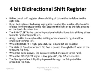
  • 1. 4 bit Bidirectional Shift Register • Bidirectional shift register allows shifting of data either to left or to the right side. • It can be implemented using logic gates circuitry that enables the transfer of data from one stage to the next stage to the right or to the left, depend on the level of control line. • The RIGHT/LEFT is the control input signal which allows data shifting either towards right or towards left. • A high on this line enables the shifting of data towards right and low enables it towards left. • When RIGHT/LEFT is high, gates G1, G2, G3 and G4 are enabled. • The state of Q output of each flip flop is passed through the D input of the following flip flop. • When the pulse arrives, the data are shifted one place to the right. • When the RIGHT/LEFT signal is low, gates G5, G6, G7 are enabled. • The Q output of each flip-flop is passed through the D input of the preceding flip-flop. 10/20/2018 Prepared By, Ms. K. D. Patil, SCOE, Kopargaon
  • 2. 4 Bit Bidirectional Shift Register 10/20/2018 Prepared By, Ms. K. D. Patil, SCOE, Kopargaon
  • 3. 4 bit Ring Counter 10/20/2018 Prepared By, Ms. K. D. Patil, SCOE, Kopargaon
  • 4. Ring Counter • Operation of Ring Counter • Initially, all the flip flops in ring counter are reset to 0 by applying CLEAR signal. Before applying the clock pulse, we apply the PRESET pulse to the flip flops which assigns the value ‘1’ to the ring counter circuit. For each clock signal, the data circulates among all the 4 flip flop stages of ring counter. • This 4 staged ring counter is called Mod 4 ring counter or 4 bit ring counter. To circulate the data correctly in the ring counter, we must load the counter with required values like all 0’s or all 1’s. 10/20/2018 Prepared By, Ms. K. D. Patil, SCOE, Kopargaon
  • 5. Ring Counter • Truth table of ring counter • When CLEAR input CLR = 0, then all flip flops are set to 1. When CLEAR input CLR = 1, the ring counter starts its operation. For one clock signal, the counter starts its operation. On next clock signal, the counter again resets to 0000. Ring counter has 4 sequences: 0001, 0010, 0100, 1000, 0000. 10/20/2018 Prepared By, Ms. K. D. Patil, SCOE, Kopargaon
  • 6. Ring Counter 10/20/2018 Prepared By, Ms. K. D. Patil, SCOE, Kopargaon
  • 7. • State diagram of ring counter • It denotes that the position of the preset digit (in this case preset digit is 1) is changing its position from LSB to MSB, for one clock signal. 10/20/2018 Prepared By, Ms. K. D. Patil, SCOE, Kopargaon
  • 8. Ring Counter • Advantages • Can be implemented using D and JK flip-flops. • It is a self-decoding circuit. It doesn’t need a decoder • Disadvantages • Only four of the 15 states are being utilized. 10/20/2018 Prepared By, Ms. K. D. Patil, SCOE, Kopargaon
  • 9. Johnson/Twisted Ring Counter • The Johnson counter is a modification of ring counter. In this the inverted output of the last stage flip flop is connected to the input of first flip flop. If we use n flip flops to design the Johnson counter, it is known as 2n bit Johnson counter or Mod 2n Johnson counter. • This is an advantage of the Johnson counter that it requires only half number of flip flops that of a ring counter uses, to design the same Mod. • The main difference between the 4 bit ring counter and the Johnson counter is that, in ring counter, we connect the output of last flip flop directly to the input of first flip flop. But in Johnson counter, we connect the inverted output of last stage to the first stage input. • The Johnson counter is also known as Twisted Ring Counter, with a feedback. In Johnson counter the input of the first flip flop is connected from the inverted output of the last flip flop. • The Johnson counter or switch trail ring counter is designed in such a way that it overcomes the limitations of ring counter. Mainly it reduces the number of flip flops required for designing the circuit. 10/20/2018 Prepared By, Ms. K. D. Patil, SCOE, Kopargaon
  • 10. 10/20/2018 Prepared By, Ms. K. D. Patil, SCOE, Kopargaon
  • 11. • Operation of johnson counter • The Johnson counter designed with D flip flop is shown in figure. It has four stages i.e. four flip flops connected in series type or cascaded. Initially zero / Null is fed to the Johnson counter and on applying the clock signal, outputs will change to “1000”, “1100”, “1110”, “1111”, “0111”, “0011”, “0001”, “0000” in a sequence and the sequence will repeat for next clock signal. • The Johnson counter produces a special pattern by passing four 0’s and then four 1’s and thus it produces a special pattern by counting up down. 10/20/2018 Prepared By, Ms. K. D. Patil, SCOE, Kopargaon
  • 12. Truth table of johnson counter 10/20/2018 Prepared By, Ms. K. D. Patil, SCOE, Kopargaon
  • 13. Timing Diagram of Johnson Ring Counter 10/20/2018 Prepared By, Ms. K. D. Patil, SCOE, Kopargaon
  • 14. State Diagram • The timing diagram of the johnson counter will explain that the clock signal changes the output of every stage of the counter, so that CLK signal will help the data to circulate from one flip flop to another. • The state diagram indicates that how the data transfers from one flip flop to another for every clock pulse. The 4 stage Johnson ring counters are used as frequency dividers, by varying their feedback connections. So they can be used as frequency divider circuits also. 10/20/2018 Prepared By, Ms. K. D. Patil, SCOE, Kopargaon
  • 15. State Diagram 10/20/2018 Prepared By, Ms. K. D. Patil, SCOE, Kopargaon
  • 16. Johnson/Twisted Ring Counter • When CLR = 0, all outputs and inputs of flip flops are preset to 0 (cleared) except the data input of right most FF which sets to 1. • When CLR = 1, Johnson counter starts its operation. On every clock edge, the output of last flip flop (1) shifts left to the third flip flop. As the first flip flop is connected to serial input i.e. 1, the input of third flip flop is 1. • In next cycle, QA = 0 so 0 rotates in ring form in second half cycle. Johnson counter has 8 sequences: 0001, 0011, 0111, 1111, 1110, 1100, 1000, and 0000. 10/20/2018 Prepared By, Ms. K. D. Patil, SCOE, Kopargaon
  • 17. Johnson/Twisted Ring Counter • Advantages • More outputs as compared to ring counter. • It has same number of flip flop but it can count twice the number of states the ring counter can count. • It count the data in a continuous loop • It only needs half the number of flip-flops compared to the standard ring counter for the same MOD • Disadvantages • Only 8 of the 15 states are being used. • It doesn’t count in a binary sequence. 10/20/2018 Prepared By, Ms. K. D. Patil, SCOE, Kopargaon
  • 18. Applications of Ring counters • Ring counters are used to count the data in a continuous loop. • They are also used to detect the various numbers values or various patterns within a set of information, by connecting AND & OR logic gates to the ring counter circuits. • 2 stage, 3 stage and 4 stage ring counters are used in frequency divider circuits as divide by 2 and divide by 3 and divide by 4 circuits, respectively. • The 3 stage Johnson counter is used as a 3 phase square wave generator which produces 1200 phase shift. • The 5 stage Johnson counter circuit is generally used as synchronous decade (BCD) counter and also as divider circuit. • The 2 stage Johnson counters are also known as “Quadrature oscillator” which is used to produce 4 level individual outputs which are out of phase with 900 with each other. This quadrature generator is used to produce 4 phase timing signal. 10/20/2018 Prepared By, Ms. K. D. Patil, SCOE, Kopargaon