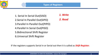
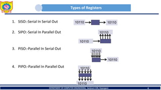
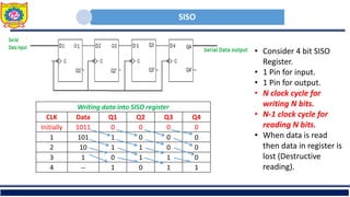
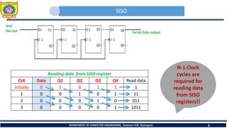
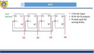
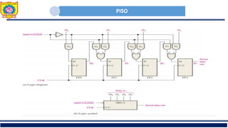
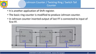
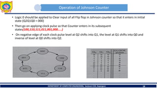
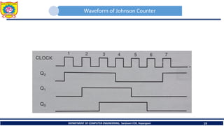
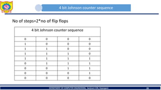
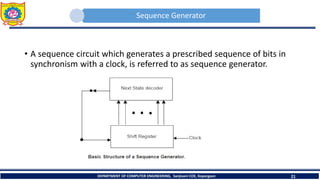
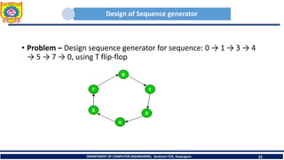
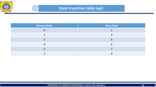
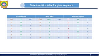
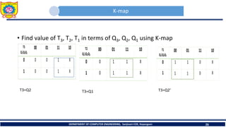
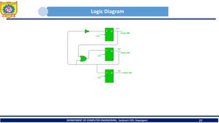
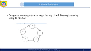
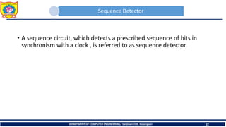
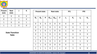
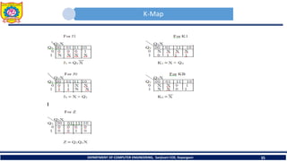
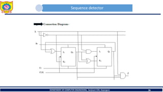
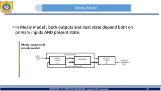
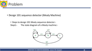
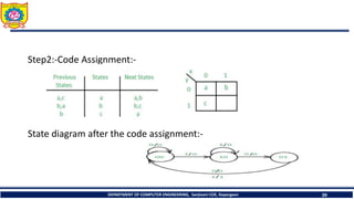
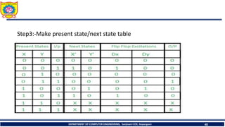
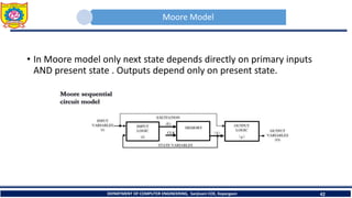
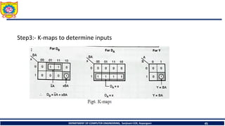
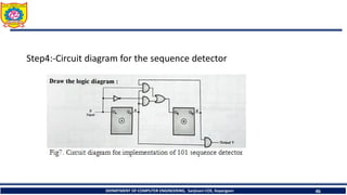
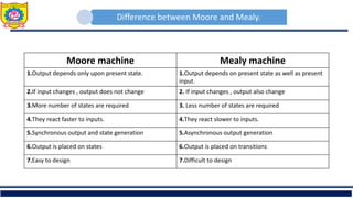
SlideShare a Scribd company logo
1 of 48
Sanjivani Rural Education Society’s
Sanjivani College of Engineering, Kopargaon-423 603
(An Autonomous Institute, Affiliated to Savitribai Phule Pune University, Pune)
NACC ‘A’ Grade Accredited, ISO 9001:2015 Certified
Department of Computer Engineering
(NBA Accredited)
Prof. S.A.Shivarkar
Assistant Professor
E-mail : shivarkarsandipcomp@sanjivani.org.in
Contact No: 8275032712
Subject- Digital Electronics and Data
Communications(CO204)
Unit 4- Sequential Circuit Design-2
Register
• Flip flop is used is store 1 bit data.
• A register is simply group of a flip-flop used to store binary number.
• Registers hold larger quantities of data than individual flip-flops.
• Registers are commonly used as temporary storage in a processor.
• Registers find application in variety of digital system including
microprocessor.
• Example
• In 8086 processor 16 bit registers are present which can store 16 bit data. (16 FF will be required)
• Not only used for storage!!
• Sequence generator
• Parallel to serial convertor
DEPARTMENT OF COMPUTER ENGINEERING, Sanjivani COE, Kopargaon 2
Types of Registers
1. Serial In Serial Out(SISO)
2.Serial In Parallel Out(SIPO)
3.Parallel In Parallel Out(PIPO)
4.Parallel In Serial Out(PISO)
5.Bidirectional Shift Register
6.Universal Shift Register
DEPARTMENT OF COMPUTER ENGINEERING, Sanjivani COE, Kopargaon 3
1. Write
2. Read
IF the registers supports Serial in or Serial out then it is called as Shift Register.
Types of Registers
DEPARTMENT OF COMPUTER ENGINEERING, Sanjivani COE, Kopargaon 4
1. SISO:-Serial In Serial Out
2. SIPO:-Serial In Parallel Out
3. PISO:-Parallel In Serial Out
4. PIPO:-Parallel In Parallel Out
10110 10110
10110
10110
10110
10110
10110
10110
SISO
Writing data into SISO register
CLK Data Q1 Q2 Q3 Q4
Initially 1011 0 0 0 0
1 101 1 0 0 0
2 10 1 1 0 0
3 1 0 1 1 0
4 -- 1 0 1 1
• Consider 4 bit SISO
Register.
• 1 Pin for input.
• 1 Pin for output.
• N clock cycle for
writing N bits.
• N-1 clock cycle for
reading N bits.
• When data is read
then data in register is
lost (Destructive
reading).
SISO
DEPARTMENT OF COMPUTER ENGINEERING, Sanjivani COE, Kopargaon 6
N-1 Clock
cycles are
required for
reading data
from SISO
registers!!
Reading data from SISO register
CLK Data Q1 Q2 Q3 Q4 Read data
Initially 0 1 0 1 1 1
1 0 0 1 0 1 11
2 0 0 0 1 0 011
3 0 0 0 0 1 1011
SIPO
• 1 Pin for input
• N Pin for N outputs
• N clock cycle for
writing N bits
PISO
PIPO
• In N bit register number of Input
pins will be N and number of
output pins will be N
• 1 clock cycle for writing N bits
Bidirectional Shift Register
DEPARTMENT OF COMPUTER ENGINEERING, Sanjivani COE, Kopargaon 10
With M=1( shift right operation):-
• 1,3,5,7 AND gates are
enabled and data DR is
shifted to the right when
clock pulses are applied.
With M=0(shift left operation):-
• 2,4,6,8 AND gates are
enabled and allowing
the data at DL to be
shifted to left
Shift
right
Shift
left
Universal Shift Registers
• If the register has both shifts(right shift and left shift) and parallel
load capabilities, it is referred to as universal shift register.
• Universal shift registers are used as memory elements in computers.
DEPARTMENT OF COMPUTER ENGINEERING, Sanjivani COE, Kopargaon 11
S1 S0 Selected Mode
0 0 No Change
0 1 Shift Right
1 0 Shift Left
1 1 Parallel Load
Universal Shift Registers
Shift Register Applications
• Temporary data storage.
• Bit manipulation.
• Serial to parallel convertor.
• Parallel to serial convertor.
• Serial and parallel communications.
• Sequence generator.
• Sequence detector.
• Logical operations.
DEPARTMENT OF COMPUTER ENGINEERING, Sanjivani COE, Kopargaon 13
Ring Counter
• It is one application of Shift Register.
• In Ring counter output of last FF is connected to the input of first FF.
• The FF are connected so that information shift from left to right and back around from Q3 to Q0
• In most cases there is single “1” in the register and it is made to circulate around the register.
DEPARTMENT OF COMPUTER ENGINEERING, Sanjivani COE, Kopargaon 14
Operation of Ring Counter
DEPARTMENT OF COMPUTER ENGINEERING, Sanjivani COE, Kopargaon 15
• Apply Logic 0 to External Input so that Ring counter enters in its initial state i.e.
(Q3Q2Q1Q0=1000).
• Then apply Logic 1 to External Input.
• Then go on applying one clock pulse so that it enters into its subsequent states as shown in
following diagrams.
• No. of states in Ring counter = No. of flip flops
Waveform of 4 bit Ring Counter
DEPARTMENT OF COMPUTER ENGINEERING, Sanjivani COE, Kopargaon 16
Johnson Counter / Twisting Ring / Switch Tail
Counter
• It is another application of Shift register.
• The basic ring counter is modified to produce Johnson counter.
• In Johnson counter inverted output of last FF is connected to input of
first FF.
DEPARTMENT OF COMPUTER ENGINEERING, Sanjivani COE, Kopargaon 17
Operation of Johnson Counter
• Logic 0 should be applied to Clear input of all Flip flop in Johnson counter so that it enters in initial
state (Q2Q1Q0 = 000)
• Then go on applying clock pulse so that Counter enters in its subsequent
states(100,110,111,011,001,000…..)
• On negative edge of each clock pulse level at Q2 shifts into Q1, the level at Q1 shifts into Q0 and
inverse of level at Q0 shifts into Q2.
DEPARTMENT OF COMPUTER ENGINEERING, Sanjivani COE, Kopargaon 18
Waveform of Johnson Counter
DEPARTMENT OF COMPUTER ENGINEERING, Sanjivani COE, Kopargaon 19
4 bit Johnson counter sequence
No of steps=2*no of flip flops
DEPARTMENT OF COMPUTER ENGINEERING, Sanjivani COE, Kopargaon 20
4 bit Johnson counter sequence
0 0 0 0
1 0 0 0
1 1 0 0
1 1 1 0
1 1 1 1
0 1 1 1
0 0 1 1
0 0 0 1
0 0 0 0
5 bit Ring counter sequence
Sequence Generator
• A sequence circuit which generates a prescribed sequence of bits in
synchronism with a clock, is referred to as sequence generator.
DEPARTMENT OF COMPUTER ENGINEERING, Sanjivani COE, Kopargaon 21
Design of Sequence generator
• Problem – Design sequence generator for sequence: 0 → 1 → 3 → 4
→ 5 → 7 → 0, using T flip-flop
DEPARTMENT OF COMPUTER ENGINEERING, Sanjivani COE, Kopargaon 22
Steps
DEPARTMENT OF COMPUTER ENGINEERING, Sanjivani COE, Kopargaon 23
• Draw Sequence
• Find no of flip flops from states
• Write state transition table
• Write flip flops inputs from state transition table
• Find equations for flip flop inputs using k-map
• Draw logic diagram
State transition table logic
Present State Next State
0 1
1 3
3 4
4 5
5 7
7 0
DEPARTMENT OF COMPUTER ENGINEERING, Sanjivani COE, Kopargaon 24
State transition table for given sequence
Present state Next state Flip flop inputs
Q3 Q2 Q1 Q3+1 Q2+1 Q1+1 T3 T2 T1
0 0 0 0 0 1 0 0 1
0 0 1 0 1 1 0 1 0
0 1 1 1 0 0 1 1 1
1 0 0 1 0 1 0 0 1
1 0 1 1 1 1 0 1 0
1 1 1 0 0 0 1 1 1
DEPARTMENT OF COMPUTER ENGINEERING, Sanjivani COE, Kopargaon 25
K-map
• Find value of T3, T2, T1 in terms of Q3, Q2, Q1 using K-map
DEPARTMENT OF COMPUTER ENGINEERING, Sanjivani COE, Kopargaon 26
T3=Q2 T3=Q1 T3=Q2’
Logic Diagram
DEPARTMENT OF COMPUTER ENGINEERING, Sanjivani COE, Kopargaon 27
Problem Statement
• Design sequence generator to go through the following states by
using JK flip-flop
DEPARTMENT OF COMPUTER ENGINEERING, Sanjivani COE, Kopargaon 28
Present
state
Next
state
J K
0 0 0 X
0 1 1 X
1 0 X 1
1 1 X 0
Present
state
Next state A B C
QA QB QC QA
+
QB
+
QC
+
JA KA JB KB JC KC
0 0 0 0 0 1 0 X 0 X 1 X
0 0 1 0 1 1 0 X 1 X X 0
0 1 0 X X X X X X X X X
0 1 1 1 0 0 1 X X 1 X 1
1 0 0 1 1 0 X 0 1 X 0 X
1 0 1 1 X X X X X X X X
1 1 0 0 0 0 X 1 X 1 0 X
1 1 1 X X X X X X X X X
State Transition
Table
K-Map
DEPARTMENT OF COMPUTER ENGINEERING, Sanjivani COE, Kopargaon 30
Connection Diagram
DEPARTMENT OF COMPUTER ENGINEERING, Sanjivani COE, Kopargaon 31
Sequence Detector
• A sequence circuit, which detects a prescribed sequence of bits in
synchronism with a clock , is referred to as sequence detector.
DEPARTMENT OF COMPUTER ENGINEERING, Sanjivani COE, Kopargaon 32
Problem statement
• Design sequence detector using JK flip flop to detect the following
sequence:- 1001
State diagram
DEPARTMENT OF COMPUTER ENGINEERING, Sanjivani COE, Kopargaon 33
DEPARTMENT OF COMPUTER ENGINEERING, Sanjivani COE, Kopargaon 34
Present
state
Next
state
J K
0 0 0 X
0 1 1 X
1 0 X 1
1 1 X 0
Present state Next state FF1 FF0
Q1 Q0 X Q1+1 Q0+1 Z J1 K1 J0 K0
0 0 0 0 0 0 0 X 0 X
0 0 1 0 1 0 0 X 1 X
0 1 0 1 0 0 1 X X 1
0 1 1 0 1 0 0 X X 0
1 0 0 1 1 0 X 0 1 X
1 0 1 0 1 0 X 1 1 X
1 1 0 0 0 0 X 1 X 1
1 1 1 0 1 1 X 1 X 0
State Transition
Table
K-Map
DEPARTMENT OF COMPUTER ENGINEERING, Sanjivani COE, Kopargaon 35
Sequence detector
DEPARTMENT OF COMPUTER ENGINEERING, Sanjivani COE, Kopargaon 36
Mealy Model
• In Mealy model , both outputs and next state depend both on
primary inputs AND present state.
DEPARTMENT OF COMPUTER ENGINEERING, Sanjivani COE, Kopargaon 37
Problem
• Design 101 sequence detector (Mealy Machine)
• Steps to design 101 Mealy sequence detector:-
Step1:- The state diagram of a Mealy machine:-
DEPARTMENT OF COMPUTER ENGINEERING, Sanjivani COE, Kopargaon 38
Step2:-Code Assignment:-
State diagram after the code assignment:-
DEPARTMENT OF COMPUTER ENGINEERING, Sanjivani COE, Kopargaon 39
Step3:-Make present state/next state table
DEPARTMENT OF COMPUTER ENGINEERING, Sanjivani COE, Kopargaon 40
Step4:-Draw K-maps and then implement the circuit
DEPARTMENT OF COMPUTER ENGINEERING, Sanjivani COE, Kopargaon 41
Moore Model
• In Moore model only next state depends directly on primary inputs
AND present state . Outputs depend only on present state.
DEPARTMENT OF COMPUTER ENGINEERING, Sanjivani COE, Kopargaon 42
Problem
• Design Moore sequence generator to detect a sequence 101
• Steps to detect a sequence 101
Step1:-The state diagram of a Moore machine for 101 detector is:
DEPARTMENT OF COMPUTER ENGINEERING, Sanjivani COE, Kopargaon 43
Step2:-State and Transition table
DEPARTMENT OF COMPUTER ENGINEERING, Sanjivani COE, Kopargaon 44
Step3:- K-maps to determine inputs
DEPARTMENT OF COMPUTER ENGINEERING, Sanjivani COE, Kopargaon 45
Step4:-Circuit diagram for the sequence detector
DEPARTMENT OF COMPUTER ENGINEERING, Sanjivani COE, Kopargaon 46
Difference between Moore and Mealy.
Moore machine Mealy machine
1.Output depends only upon present state. 1.Output depends on present state as well as present
input.
2.If input changes , output does not change 2. If input changes , output also change
3.More number of states are required 3. Less number of states are required
4.They react faster to inputs. 4.They react slower to inputs.
5.Synchronous output and state generation 5.Asynchronous output generation
6.Output is placed on states 6.Output is placed on transitions
7.Easy to design 7.Difficult to design
THANKYOU…………………
DEPARTMENT OF COMPUTER ENGINEERING, Sanjivani COE, Kopargaon 48

More Related Content

Similar to Sequential Circuit Design-2.pdf

DELD Unit IV ring and twisted ring counter
DELD Unit IV ring and twisted ring counterDELD Unit IV ring and twisted ring counter
DELD Unit IV ring and twisted ring counterKanchanPatil34
 
Digital logic and microprocessors
Digital logic and microprocessorsDigital logic and microprocessors
Digital logic and microprocessorsMilind Pelagade
 
Chapter 7_Counters (EEEg4302).pdf
Chapter 7_Counters (EEEg4302).pdfChapter 7_Counters (EEEg4302).pdf
Chapter 7_Counters (EEEg4302).pdfTamiratDejene1
 
Counter - by Zakariya Hossain
Counter - by Zakariya HossainCounter - by Zakariya Hossain
Counter - by Zakariya HossainZakariya Hossain
 
Eceg 3201-dld-lec 11-registers_and_asynchoronous_counters
Eceg 3201-dld-lec 11-registers_and_asynchoronous_countersEceg 3201-dld-lec 11-registers_and_asynchoronous_counters
Eceg 3201-dld-lec 11-registers_and_asynchoronous_countersNebiyu Musie
 
Eceg 3201-dld-lec 12-synchronous_counter_design
Eceg 3201-dld-lec 12-synchronous_counter_designEceg 3201-dld-lec 12-synchronous_counter_design
Eceg 3201-dld-lec 12-synchronous_counter_designNebiyu Musie
 
FYBSC IT Digital Electronics Unit V Chapter I Counters
FYBSC IT Digital Electronics Unit V Chapter I CountersFYBSC IT Digital Electronics Unit V Chapter I Counters
FYBSC IT Digital Electronics Unit V Chapter I CountersArti Parab Academics
 
counters and registers
counters and registerscounters and registers
counters and registersMeenaAnusha1
 
counters_and_registers_5 lecture fifth.ppt
counters_and_registers_5 lecture fifth.pptcounters_and_registers_5 lecture fifth.ppt
counters_and_registers_5 lecture fifth.pptImranAhmadAhmad
 
Digital Clock Using Logic Gates
Digital Clock Using Logic GatesDigital Clock Using Logic Gates
Digital Clock Using Logic GatesJalpaMaheshwari1
 
Sequential circuit-flip flops
Sequential circuit-flip flopsSequential circuit-flip flops
Sequential circuit-flip flopsDr Naim R Kidwai
 
Ade(unit 4) Counters
Ade(unit 4) CountersAde(unit 4) Counters
Ade(unit 4) CountersANKITSURWADE
 
Analysis sequential circuits
Analysis sequential circuitsAnalysis sequential circuits
Analysis sequential circuitsG Subramaniamg
 
digital elctronics
digital elctronicsdigital elctronics
digital elctronicsAsif Iqbal
 

Similar to Sequential Circuit Design-2.pdf (20)

DELD Unit IV ring and twisted ring counter
DELD Unit IV ring and twisted ring counterDELD Unit IV ring and twisted ring counter
DELD Unit IV ring and twisted ring counter
 
Chapter 6 register
Chapter 6 registerChapter 6 register
Chapter 6 register
 
Digital logic and microprocessors
Digital logic and microprocessorsDigital logic and microprocessors
Digital logic and microprocessors
 
Chapter 7_Counters (EEEg4302).pdf
Chapter 7_Counters (EEEg4302).pdfChapter 7_Counters (EEEg4302).pdf
Chapter 7_Counters (EEEg4302).pdf
 
Counters
CountersCounters
Counters
 
4 bit Binary counter
4 bit Binary counter4 bit Binary counter
4 bit Binary counter
 
Counter - by Zakariya Hossain
Counter - by Zakariya HossainCounter - by Zakariya Hossain
Counter - by Zakariya Hossain
 
Eceg 3201-dld-lec 11-registers_and_asynchoronous_counters
Eceg 3201-dld-lec 11-registers_and_asynchoronous_countersEceg 3201-dld-lec 11-registers_and_asynchoronous_counters
Eceg 3201-dld-lec 11-registers_and_asynchoronous_counters
 
Sequential Logic
Sequential LogicSequential Logic
Sequential Logic
 
Eceg 3201-dld-lec 12-synchronous_counter_design
Eceg 3201-dld-lec 12-synchronous_counter_designEceg 3201-dld-lec 12-synchronous_counter_design
Eceg 3201-dld-lec 12-synchronous_counter_design
 
Bds lab 4
Bds lab 4Bds lab 4
Bds lab 4
 
FYBSC IT Digital Electronics Unit V Chapter I Counters
FYBSC IT Digital Electronics Unit V Chapter I CountersFYBSC IT Digital Electronics Unit V Chapter I Counters
FYBSC IT Digital Electronics Unit V Chapter I Counters
 
counters and registers
counters and registerscounters and registers
counters and registers
 
counters_and_registers_5 lecture fifth.ppt
counters_and_registers_5 lecture fifth.pptcounters_and_registers_5 lecture fifth.ppt
counters_and_registers_5 lecture fifth.ppt
 
digital Counter
digital Counterdigital Counter
digital Counter
 
Digital Clock Using Logic Gates
Digital Clock Using Logic GatesDigital Clock Using Logic Gates
Digital Clock Using Logic Gates
 
Sequential circuit-flip flops
Sequential circuit-flip flopsSequential circuit-flip flops
Sequential circuit-flip flops
 
Ade(unit 4) Counters
Ade(unit 4) CountersAde(unit 4) Counters
Ade(unit 4) Counters
 
Analysis sequential circuits
Analysis sequential circuitsAnalysis sequential circuits
Analysis sequential circuits
 
digital elctronics
digital elctronicsdigital elctronics
digital elctronics
 

More from ShivarkarSandip

Classification, Attribute Selection, Classifiers- Decision Tree, ID3,C4.5,Nav...
Classification, Attribute Selection, Classifiers- Decision Tree, ID3,C4.5,Nav...Classification, Attribute Selection, Classifiers- Decision Tree, ID3,C4.5,Nav...
Classification, Attribute Selection, Classifiers- Decision Tree, ID3,C4.5,Nav...ShivarkarSandip
 
Frequent Pattern Analysis, Apriori and FP Growth Algorithm
Frequent Pattern Analysis, Apriori and FP Growth AlgorithmFrequent Pattern Analysis, Apriori and FP Growth Algorithm
Frequent Pattern Analysis, Apriori and FP Growth AlgorithmShivarkarSandip
 
Data Warehouse and Architecture, OLAP Operation
Data Warehouse and Architecture, OLAP OperationData Warehouse and Architecture, OLAP Operation
Data Warehouse and Architecture, OLAP OperationShivarkarSandip
 
Data Preparation and Preprocessing , Data Cleaning
Data Preparation and Preprocessing , Data CleaningData Preparation and Preprocessing , Data Cleaning
Data Preparation and Preprocessing , Data CleaningShivarkarSandip
 
Introduction to Data Mining, KDD Process, OLTP and OLAP
Introduction to Data Mining, KDD Process, OLTP and OLAPIntroduction to Data Mining, KDD Process, OLTP and OLAP
Introduction to Data Mining, KDD Process, OLTP and OLAPShivarkarSandip
 
Introduction to Data Mining KDD Process OLAP
Introduction to Data Mining KDD Process OLAPIntroduction to Data Mining KDD Process OLAP
Introduction to Data Mining KDD Process OLAPShivarkarSandip
 
Issues in data mining Patterns Online Analytical Processing
Issues in data mining  Patterns Online Analytical ProcessingIssues in data mining  Patterns Online Analytical Processing
Issues in data mining Patterns Online Analytical ProcessingShivarkarSandip
 
Introduction to data mining which covers the basics
Introduction to data mining which covers the basicsIntroduction to data mining which covers the basics
Introduction to data mining which covers the basicsShivarkarSandip
 
Introduction to Data Communication.pdf
Introduction to Data Communication.pdfIntroduction to Data Communication.pdf
Introduction to Data Communication.pdfShivarkarSandip
 
Classification of Signal.pdf
Classification of Signal.pdfClassification of Signal.pdf
Classification of Signal.pdfShivarkarSandip
 
Boolean Algebra Terminologies.pdf
Boolean Algebra Terminologies.pdfBoolean Algebra Terminologies.pdf
Boolean Algebra Terminologies.pdfShivarkarSandip
 
Unit III Introduction to DWH.pdf
Unit III Introduction to DWH.pdfUnit III Introduction to DWH.pdf
Unit III Introduction to DWH.pdfShivarkarSandip
 
Unit II Decision Making Basics and Concepts.pdf
Unit II Decision Making Basics and Concepts.pdfUnit II Decision Making Basics and Concepts.pdf
Unit II Decision Making Basics and Concepts.pdfShivarkarSandip
 
Unit I Factors Responsible for Successful BI Project.pdf
Unit I Factors Responsible for Successful BI Project.pdfUnit I Factors Responsible for Successful BI Project.pdf
Unit I Factors Responsible for Successful BI Project.pdfShivarkarSandip
 
Unit I Operational data Informational data.pdf
Unit I Operational data  Informational data.pdfUnit I Operational data  Informational data.pdf
Unit I Operational data Informational data.pdfShivarkarSandip
 
Unit I Introduction to BI.pdf
Unit I Introduction to BI.pdfUnit I Introduction to BI.pdf
Unit I Introduction to BI.pdfShivarkarSandip
 
Unit III Components and Arch of DWH ETL Process.pdf
Unit III  Components and Arch of DWH ETL Process.pdfUnit III  Components and Arch of DWH ETL Process.pdf
Unit III Components and Arch of DWH ETL Process.pdfShivarkarSandip
 
Unit I Role of Mathematical Model in BI and BI Cycle.pdf
Unit I Role of Mathematical Model in BI and BI Cycle.pdfUnit I Role of Mathematical Model in BI and BI Cycle.pdf
Unit I Role of Mathematical Model in BI and BI Cycle.pdfShivarkarSandip
 
Unit II Decision Support System.pdf
Unit II Decision Support System.pdfUnit II Decision Support System.pdf
Unit II Decision Support System.pdfShivarkarSandip
 

More from ShivarkarSandip (20)

Classification, Attribute Selection, Classifiers- Decision Tree, ID3,C4.5,Nav...
Classification, Attribute Selection, Classifiers- Decision Tree, ID3,C4.5,Nav...Classification, Attribute Selection, Classifiers- Decision Tree, ID3,C4.5,Nav...
Classification, Attribute Selection, Classifiers- Decision Tree, ID3,C4.5,Nav...
 
Frequent Pattern Analysis, Apriori and FP Growth Algorithm
Frequent Pattern Analysis, Apriori and FP Growth AlgorithmFrequent Pattern Analysis, Apriori and FP Growth Algorithm
Frequent Pattern Analysis, Apriori and FP Growth Algorithm
 
Data Warehouse and Architecture, OLAP Operation
Data Warehouse and Architecture, OLAP OperationData Warehouse and Architecture, OLAP Operation
Data Warehouse and Architecture, OLAP Operation
 
Data Preparation and Preprocessing , Data Cleaning
Data Preparation and Preprocessing , Data CleaningData Preparation and Preprocessing , Data Cleaning
Data Preparation and Preprocessing , Data Cleaning
 
Introduction to Data Mining, KDD Process, OLTP and OLAP
Introduction to Data Mining, KDD Process, OLTP and OLAPIntroduction to Data Mining, KDD Process, OLTP and OLAP
Introduction to Data Mining, KDD Process, OLTP and OLAP
 
Introduction to Data Mining KDD Process OLAP
Introduction to Data Mining KDD Process OLAPIntroduction to Data Mining KDD Process OLAP
Introduction to Data Mining KDD Process OLAP
 
Issues in data mining Patterns Online Analytical Processing
Issues in data mining  Patterns Online Analytical ProcessingIssues in data mining  Patterns Online Analytical Processing
Issues in data mining Patterns Online Analytical Processing
 
Introduction to data mining which covers the basics
Introduction to data mining which covers the basicsIntroduction to data mining which covers the basics
Introduction to data mining which covers the basics
 
Introduction to Data Communication.pdf
Introduction to Data Communication.pdfIntroduction to Data Communication.pdf
Introduction to Data Communication.pdf
 
Classification of Signal.pdf
Classification of Signal.pdfClassification of Signal.pdf
Classification of Signal.pdf
 
Boolean Algebra Terminologies.pdf
Boolean Algebra Terminologies.pdfBoolean Algebra Terminologies.pdf
Boolean Algebra Terminologies.pdf
 
Logic Minimization.pdf
Logic Minimization.pdfLogic Minimization.pdf
Logic Minimization.pdf
 
Unit III Introduction to DWH.pdf
Unit III Introduction to DWH.pdfUnit III Introduction to DWH.pdf
Unit III Introduction to DWH.pdf
 
Unit II Decision Making Basics and Concepts.pdf
Unit II Decision Making Basics and Concepts.pdfUnit II Decision Making Basics and Concepts.pdf
Unit II Decision Making Basics and Concepts.pdf
 
Unit I Factors Responsible for Successful BI Project.pdf
Unit I Factors Responsible for Successful BI Project.pdfUnit I Factors Responsible for Successful BI Project.pdf
Unit I Factors Responsible for Successful BI Project.pdf
 
Unit I Operational data Informational data.pdf
Unit I Operational data  Informational data.pdfUnit I Operational data  Informational data.pdf
Unit I Operational data Informational data.pdf
 
Unit I Introduction to BI.pdf
Unit I Introduction to BI.pdfUnit I Introduction to BI.pdf
Unit I Introduction to BI.pdf
 
Unit III Components and Arch of DWH ETL Process.pdf
Unit III  Components and Arch of DWH ETL Process.pdfUnit III  Components and Arch of DWH ETL Process.pdf
Unit III Components and Arch of DWH ETL Process.pdf
 
Unit I Role of Mathematical Model in BI and BI Cycle.pdf
Unit I Role of Mathematical Model in BI and BI Cycle.pdfUnit I Role of Mathematical Model in BI and BI Cycle.pdf
Unit I Role of Mathematical Model in BI and BI Cycle.pdf
 
Unit II Decision Support System.pdf
Unit II Decision Support System.pdfUnit II Decision Support System.pdf
Unit II Decision Support System.pdf
 

Recently uploaded

Booking open Available Pune Call Girls Koregaon Park 6297143586 Call Hot Ind...
Booking open Available Pune Call Girls Koregaon Park  6297143586 Call Hot Ind...Booking open Available Pune Call Girls Koregaon Park  6297143586 Call Hot Ind...
Booking open Available Pune Call Girls Koregaon Park 6297143586 Call Hot Ind...Call Girls in Nagpur High Profile
 
(RIA) Call Girls Bhosari ( 7001035870 ) HI-Fi Pune Escorts Service
(RIA) Call Girls Bhosari ( 7001035870 ) HI-Fi Pune Escorts Service(RIA) Call Girls Bhosari ( 7001035870 ) HI-Fi Pune Escorts Service
(RIA) Call Girls Bhosari ( 7001035870 ) HI-Fi Pune Escorts Serviceranjana rawat
 
VIP Call Girls Service Hitech City Hyderabad Call +91-8250192130
VIP Call Girls Service Hitech City Hyderabad Call +91-8250192130VIP Call Girls Service Hitech City Hyderabad Call +91-8250192130
VIP Call Girls Service Hitech City Hyderabad Call +91-8250192130Suhani Kapoor
 
HARMONY IN THE NATURE AND EXISTENCE - Unit-IV
HARMONY IN THE NATURE AND EXISTENCE - Unit-IVHARMONY IN THE NATURE AND EXISTENCE - Unit-IV
HARMONY IN THE NATURE AND EXISTENCE - Unit-IVRajaP95
 
Introduction to IEEE STANDARDS and its different types.pptx
Introduction to IEEE STANDARDS and its different types.pptxIntroduction to IEEE STANDARDS and its different types.pptx
Introduction to IEEE STANDARDS and its different types.pptxupamatechverse
 
Software Development Life Cycle By Team Orange (Dept. of Pharmacy)
Software Development Life Cycle By  Team Orange (Dept. of Pharmacy)Software Development Life Cycle By  Team Orange (Dept. of Pharmacy)
Software Development Life Cycle By Team Orange (Dept. of Pharmacy)Suman Mia
 
Introduction to Multiple Access Protocol.pptx
Introduction to Multiple Access Protocol.pptxIntroduction to Multiple Access Protocol.pptx
Introduction to Multiple Access Protocol.pptxupamatechverse
 
Call Girls Service Nashik Vaishnavi 7001305949 Independent Escort Service Nashik
Call Girls Service Nashik Vaishnavi 7001305949 Independent Escort Service NashikCall Girls Service Nashik Vaishnavi 7001305949 Independent Escort Service Nashik
Call Girls Service Nashik Vaishnavi 7001305949 Independent Escort Service NashikCall Girls in Nagpur High Profile
 
Call Girls in Nagpur Suman Call 7001035870 Meet With Nagpur Escorts
Call Girls in Nagpur Suman Call 7001035870 Meet With Nagpur EscortsCall Girls in Nagpur Suman Call 7001035870 Meet With Nagpur Escorts
Call Girls in Nagpur Suman Call 7001035870 Meet With Nagpur EscortsCall Girls in Nagpur High Profile
 
High Profile Call Girls Nagpur Isha Call 7001035870 Meet With Nagpur Escorts
High Profile Call Girls Nagpur Isha Call 7001035870 Meet With Nagpur EscortsHigh Profile Call Girls Nagpur Isha Call 7001035870 Meet With Nagpur Escorts
High Profile Call Girls Nagpur Isha Call 7001035870 Meet With Nagpur Escortsranjana rawat
 
(ANVI) Koregaon Park Call Girls Just Call 7001035870 [ Cash on Delivery ] Pun...
(ANVI) Koregaon Park Call Girls Just Call 7001035870 [ Cash on Delivery ] Pun...(ANVI) Koregaon Park Call Girls Just Call 7001035870 [ Cash on Delivery ] Pun...
(ANVI) Koregaon Park Call Girls Just Call 7001035870 [ Cash on Delivery ] Pun...ranjana rawat
 
Call for Papers - African Journal of Biological Sciences, E-ISSN: 2663-2187, ...
Call for Papers - African Journal of Biological Sciences, E-ISSN: 2663-2187, ...Call for Papers - African Journal of Biological Sciences, E-ISSN: 2663-2187, ...
Call for Papers - African Journal of Biological Sciences, E-ISSN: 2663-2187, ...Christo Ananth
 
SPICE PARK APR2024 ( 6,793 SPICE Models )
SPICE PARK APR2024 ( 6,793 SPICE Models )SPICE PARK APR2024 ( 6,793 SPICE Models )
SPICE PARK APR2024 ( 6,793 SPICE Models )Tsuyoshi Horigome
 
The Most Attractive Pune Call Girls Budhwar Peth 8250192130 Will You Miss Thi...
The Most Attractive Pune Call Girls Budhwar Peth 8250192130 Will You Miss Thi...The Most Attractive Pune Call Girls Budhwar Peth 8250192130 Will You Miss Thi...
The Most Attractive Pune Call Girls Budhwar Peth 8250192130 Will You Miss Thi...ranjana rawat
 
MANUFACTURING PROCESS-II UNIT-5 NC MACHINE TOOLS
MANUFACTURING PROCESS-II UNIT-5 NC MACHINE TOOLSMANUFACTURING PROCESS-II UNIT-5 NC MACHINE TOOLS
MANUFACTURING PROCESS-II UNIT-5 NC MACHINE TOOLSSIVASHANKAR N
 
Structural Analysis and Design of Foundations: A Comprehensive Handbook for S...
Structural Analysis and Design of Foundations: A Comprehensive Handbook for S...Structural Analysis and Design of Foundations: A Comprehensive Handbook for S...
Structural Analysis and Design of Foundations: A Comprehensive Handbook for S...Dr.Costas Sachpazis
 
Porous Ceramics seminar and technical writing
Porous Ceramics seminar and technical writingPorous Ceramics seminar and technical writing
Porous Ceramics seminar and technical writingrakeshbaidya232001
 
Coefficient of Thermal Expansion and their Importance.pptx
Coefficient of Thermal Expansion and their Importance.pptxCoefficient of Thermal Expansion and their Importance.pptx
Coefficient of Thermal Expansion and their Importance.pptxAsutosh Ranjan
 

Recently uploaded (20)

Booking open Available Pune Call Girls Koregaon Park 6297143586 Call Hot Ind...
Booking open Available Pune Call Girls Koregaon Park  6297143586 Call Hot Ind...Booking open Available Pune Call Girls Koregaon Park  6297143586 Call Hot Ind...
Booking open Available Pune Call Girls Koregaon Park 6297143586 Call Hot Ind...
 
(RIA) Call Girls Bhosari ( 7001035870 ) HI-Fi Pune Escorts Service
(RIA) Call Girls Bhosari ( 7001035870 ) HI-Fi Pune Escorts Service(RIA) Call Girls Bhosari ( 7001035870 ) HI-Fi Pune Escorts Service
(RIA) Call Girls Bhosari ( 7001035870 ) HI-Fi Pune Escorts Service
 
VIP Call Girls Service Hitech City Hyderabad Call +91-8250192130
VIP Call Girls Service Hitech City Hyderabad Call +91-8250192130VIP Call Girls Service Hitech City Hyderabad Call +91-8250192130
VIP Call Girls Service Hitech City Hyderabad Call +91-8250192130
 
HARMONY IN THE NATURE AND EXISTENCE - Unit-IV
HARMONY IN THE NATURE AND EXISTENCE - Unit-IVHARMONY IN THE NATURE AND EXISTENCE - Unit-IV
HARMONY IN THE NATURE AND EXISTENCE - Unit-IV
 
DJARUM4D - SLOT GACOR ONLINE | SLOT DEMO ONLINE
DJARUM4D - SLOT GACOR ONLINE | SLOT DEMO ONLINEDJARUM4D - SLOT GACOR ONLINE | SLOT DEMO ONLINE
DJARUM4D - SLOT GACOR ONLINE | SLOT DEMO ONLINE
 
Introduction to IEEE STANDARDS and its different types.pptx
Introduction to IEEE STANDARDS and its different types.pptxIntroduction to IEEE STANDARDS and its different types.pptx
Introduction to IEEE STANDARDS and its different types.pptx
 
Software Development Life Cycle By Team Orange (Dept. of Pharmacy)
Software Development Life Cycle By  Team Orange (Dept. of Pharmacy)Software Development Life Cycle By  Team Orange (Dept. of Pharmacy)
Software Development Life Cycle By Team Orange (Dept. of Pharmacy)
 
Introduction to Multiple Access Protocol.pptx
Introduction to Multiple Access Protocol.pptxIntroduction to Multiple Access Protocol.pptx
Introduction to Multiple Access Protocol.pptx
 
Call Girls Service Nashik Vaishnavi 7001305949 Independent Escort Service Nashik
Call Girls Service Nashik Vaishnavi 7001305949 Independent Escort Service NashikCall Girls Service Nashik Vaishnavi 7001305949 Independent Escort Service Nashik
Call Girls Service Nashik Vaishnavi 7001305949 Independent Escort Service Nashik
 
Call Girls in Nagpur Suman Call 7001035870 Meet With Nagpur Escorts
Call Girls in Nagpur Suman Call 7001035870 Meet With Nagpur EscortsCall Girls in Nagpur Suman Call 7001035870 Meet With Nagpur Escorts
Call Girls in Nagpur Suman Call 7001035870 Meet With Nagpur Escorts
 
High Profile Call Girls Nagpur Isha Call 7001035870 Meet With Nagpur Escorts
High Profile Call Girls Nagpur Isha Call 7001035870 Meet With Nagpur EscortsHigh Profile Call Girls Nagpur Isha Call 7001035870 Meet With Nagpur Escorts
High Profile Call Girls Nagpur Isha Call 7001035870 Meet With Nagpur Escorts
 
(ANVI) Koregaon Park Call Girls Just Call 7001035870 [ Cash on Delivery ] Pun...
(ANVI) Koregaon Park Call Girls Just Call 7001035870 [ Cash on Delivery ] Pun...(ANVI) Koregaon Park Call Girls Just Call 7001035870 [ Cash on Delivery ] Pun...
(ANVI) Koregaon Park Call Girls Just Call 7001035870 [ Cash on Delivery ] Pun...
 
Call for Papers - African Journal of Biological Sciences, E-ISSN: 2663-2187, ...
Call for Papers - African Journal of Biological Sciences, E-ISSN: 2663-2187, ...Call for Papers - African Journal of Biological Sciences, E-ISSN: 2663-2187, ...
Call for Papers - African Journal of Biological Sciences, E-ISSN: 2663-2187, ...
 
SPICE PARK APR2024 ( 6,793 SPICE Models )
SPICE PARK APR2024 ( 6,793 SPICE Models )SPICE PARK APR2024 ( 6,793 SPICE Models )
SPICE PARK APR2024 ( 6,793 SPICE Models )
 
Roadmap to Membership of RICS - Pathways and Routes
Roadmap to Membership of RICS - Pathways and RoutesRoadmap to Membership of RICS - Pathways and Routes
Roadmap to Membership of RICS - Pathways and Routes
 
The Most Attractive Pune Call Girls Budhwar Peth 8250192130 Will You Miss Thi...
The Most Attractive Pune Call Girls Budhwar Peth 8250192130 Will You Miss Thi...The Most Attractive Pune Call Girls Budhwar Peth 8250192130 Will You Miss Thi...
The Most Attractive Pune Call Girls Budhwar Peth 8250192130 Will You Miss Thi...
 
MANUFACTURING PROCESS-II UNIT-5 NC MACHINE TOOLS
MANUFACTURING PROCESS-II UNIT-5 NC MACHINE TOOLSMANUFACTURING PROCESS-II UNIT-5 NC MACHINE TOOLS
MANUFACTURING PROCESS-II UNIT-5 NC MACHINE TOOLS
 
Structural Analysis and Design of Foundations: A Comprehensive Handbook for S...
Structural Analysis and Design of Foundations: A Comprehensive Handbook for S...Structural Analysis and Design of Foundations: A Comprehensive Handbook for S...
Structural Analysis and Design of Foundations: A Comprehensive Handbook for S...
 
Porous Ceramics seminar and technical writing
Porous Ceramics seminar and technical writingPorous Ceramics seminar and technical writing
Porous Ceramics seminar and technical writing
 
Coefficient of Thermal Expansion and their Importance.pptx
Coefficient of Thermal Expansion and their Importance.pptxCoefficient of Thermal Expansion and their Importance.pptx
Coefficient of Thermal Expansion and their Importance.pptx
 

Sequential Circuit Design-2.pdf

  • 1. Sanjivani Rural Education Society’s Sanjivani College of Engineering, Kopargaon-423 603 (An Autonomous Institute, Affiliated to Savitribai Phule Pune University, Pune) NACC ‘A’ Grade Accredited, ISO 9001:2015 Certified Department of Computer Engineering (NBA Accredited) Prof. S.A.Shivarkar Assistant Professor E-mail : shivarkarsandipcomp@sanjivani.org.in Contact No: 8275032712 Subject- Digital Electronics and Data Communications(CO204) Unit 4- Sequential Circuit Design-2
  • 2. Register • Flip flop is used is store 1 bit data. • A register is simply group of a flip-flop used to store binary number. • Registers hold larger quantities of data than individual flip-flops. • Registers are commonly used as temporary storage in a processor. • Registers find application in variety of digital system including microprocessor. • Example • In 8086 processor 16 bit registers are present which can store 16 bit data. (16 FF will be required) • Not only used for storage!! • Sequence generator • Parallel to serial convertor DEPARTMENT OF COMPUTER ENGINEERING, Sanjivani COE, Kopargaon 2
  • 3. Types of Registers 1. Serial In Serial Out(SISO) 2.Serial In Parallel Out(SIPO) 3.Parallel In Parallel Out(PIPO) 4.Parallel In Serial Out(PISO) 5.Bidirectional Shift Register 6.Universal Shift Register DEPARTMENT OF COMPUTER ENGINEERING, Sanjivani COE, Kopargaon 3 1. Write 2. Read IF the registers supports Serial in or Serial out then it is called as Shift Register.
  • 4. Types of Registers DEPARTMENT OF COMPUTER ENGINEERING, Sanjivani COE, Kopargaon 4 1. SISO:-Serial In Serial Out 2. SIPO:-Serial In Parallel Out 3. PISO:-Parallel In Serial Out 4. PIPO:-Parallel In Parallel Out 10110 10110 10110 10110 10110 10110 10110 10110
  • 5. SISO Writing data into SISO register CLK Data Q1 Q2 Q3 Q4 Initially 1011 0 0 0 0 1 101 1 0 0 0 2 10 1 1 0 0 3 1 0 1 1 0 4 -- 1 0 1 1 • Consider 4 bit SISO Register. • 1 Pin for input. • 1 Pin for output. • N clock cycle for writing N bits. • N-1 clock cycle for reading N bits. • When data is read then data in register is lost (Destructive reading).
  • 6. SISO DEPARTMENT OF COMPUTER ENGINEERING, Sanjivani COE, Kopargaon 6 N-1 Clock cycles are required for reading data from SISO registers!! Reading data from SISO register CLK Data Q1 Q2 Q3 Q4 Read data Initially 0 1 0 1 1 1 1 0 0 1 0 1 11 2 0 0 0 1 0 011 3 0 0 0 0 1 1011
  • 7. SIPO • 1 Pin for input • N Pin for N outputs • N clock cycle for writing N bits
  • 9. PIPO • In N bit register number of Input pins will be N and number of output pins will be N • 1 clock cycle for writing N bits
  • 10. Bidirectional Shift Register DEPARTMENT OF COMPUTER ENGINEERING, Sanjivani COE, Kopargaon 10 With M=1( shift right operation):- • 1,3,5,7 AND gates are enabled and data DR is shifted to the right when clock pulses are applied. With M=0(shift left operation):- • 2,4,6,8 AND gates are enabled and allowing the data at DL to be shifted to left Shift right Shift left
  • 11. Universal Shift Registers • If the register has both shifts(right shift and left shift) and parallel load capabilities, it is referred to as universal shift register. • Universal shift registers are used as memory elements in computers. DEPARTMENT OF COMPUTER ENGINEERING, Sanjivani COE, Kopargaon 11 S1 S0 Selected Mode 0 0 No Change 0 1 Shift Right 1 0 Shift Left 1 1 Parallel Load
  • 13. Shift Register Applications • Temporary data storage. • Bit manipulation. • Serial to parallel convertor. • Parallel to serial convertor. • Serial and parallel communications. • Sequence generator. • Sequence detector. • Logical operations. DEPARTMENT OF COMPUTER ENGINEERING, Sanjivani COE, Kopargaon 13
  • 14. Ring Counter • It is one application of Shift Register. • In Ring counter output of last FF is connected to the input of first FF. • The FF are connected so that information shift from left to right and back around from Q3 to Q0 • In most cases there is single “1” in the register and it is made to circulate around the register. DEPARTMENT OF COMPUTER ENGINEERING, Sanjivani COE, Kopargaon 14
  • 15. Operation of Ring Counter DEPARTMENT OF COMPUTER ENGINEERING, Sanjivani COE, Kopargaon 15 • Apply Logic 0 to External Input so that Ring counter enters in its initial state i.e. (Q3Q2Q1Q0=1000). • Then apply Logic 1 to External Input. • Then go on applying one clock pulse so that it enters into its subsequent states as shown in following diagrams. • No. of states in Ring counter = No. of flip flops
  • 16. Waveform of 4 bit Ring Counter DEPARTMENT OF COMPUTER ENGINEERING, Sanjivani COE, Kopargaon 16
  • 17. Johnson Counter / Twisting Ring / Switch Tail Counter • It is another application of Shift register. • The basic ring counter is modified to produce Johnson counter. • In Johnson counter inverted output of last FF is connected to input of first FF. DEPARTMENT OF COMPUTER ENGINEERING, Sanjivani COE, Kopargaon 17
  • 18. Operation of Johnson Counter • Logic 0 should be applied to Clear input of all Flip flop in Johnson counter so that it enters in initial state (Q2Q1Q0 = 000) • Then go on applying clock pulse so that Counter enters in its subsequent states(100,110,111,011,001,000…..) • On negative edge of each clock pulse level at Q2 shifts into Q1, the level at Q1 shifts into Q0 and inverse of level at Q0 shifts into Q2. DEPARTMENT OF COMPUTER ENGINEERING, Sanjivani COE, Kopargaon 18
  • 19. Waveform of Johnson Counter DEPARTMENT OF COMPUTER ENGINEERING, Sanjivani COE, Kopargaon 19
  • 20. 4 bit Johnson counter sequence No of steps=2*no of flip flops DEPARTMENT OF COMPUTER ENGINEERING, Sanjivani COE, Kopargaon 20 4 bit Johnson counter sequence 0 0 0 0 1 0 0 0 1 1 0 0 1 1 1 0 1 1 1 1 0 1 1 1 0 0 1 1 0 0 0 1 0 0 0 0 5 bit Ring counter sequence
  • 21. Sequence Generator • A sequence circuit which generates a prescribed sequence of bits in synchronism with a clock, is referred to as sequence generator. DEPARTMENT OF COMPUTER ENGINEERING, Sanjivani COE, Kopargaon 21
  • 22. Design of Sequence generator • Problem – Design sequence generator for sequence: 0 → 1 → 3 → 4 → 5 → 7 → 0, using T flip-flop DEPARTMENT OF COMPUTER ENGINEERING, Sanjivani COE, Kopargaon 22
  • 23. Steps DEPARTMENT OF COMPUTER ENGINEERING, Sanjivani COE, Kopargaon 23 • Draw Sequence • Find no of flip flops from states • Write state transition table • Write flip flops inputs from state transition table • Find equations for flip flop inputs using k-map • Draw logic diagram
  • 24. State transition table logic Present State Next State 0 1 1 3 3 4 4 5 5 7 7 0 DEPARTMENT OF COMPUTER ENGINEERING, Sanjivani COE, Kopargaon 24
  • 25. State transition table for given sequence Present state Next state Flip flop inputs Q3 Q2 Q1 Q3+1 Q2+1 Q1+1 T3 T2 T1 0 0 0 0 0 1 0 0 1 0 0 1 0 1 1 0 1 0 0 1 1 1 0 0 1 1 1 1 0 0 1 0 1 0 0 1 1 0 1 1 1 1 0 1 0 1 1 1 0 0 0 1 1 1 DEPARTMENT OF COMPUTER ENGINEERING, Sanjivani COE, Kopargaon 25
  • 26. K-map • Find value of T3, T2, T1 in terms of Q3, Q2, Q1 using K-map DEPARTMENT OF COMPUTER ENGINEERING, Sanjivani COE, Kopargaon 26 T3=Q2 T3=Q1 T3=Q2’
  • 27. Logic Diagram DEPARTMENT OF COMPUTER ENGINEERING, Sanjivani COE, Kopargaon 27
  • 28. Problem Statement • Design sequence generator to go through the following states by using JK flip-flop DEPARTMENT OF COMPUTER ENGINEERING, Sanjivani COE, Kopargaon 28
  • 29. Present state Next state J K 0 0 0 X 0 1 1 X 1 0 X 1 1 1 X 0 Present state Next state A B C QA QB QC QA + QB + QC + JA KA JB KB JC KC 0 0 0 0 0 1 0 X 0 X 1 X 0 0 1 0 1 1 0 X 1 X X 0 0 1 0 X X X X X X X X X 0 1 1 1 0 0 1 X X 1 X 1 1 0 0 1 1 0 X 0 1 X 0 X 1 0 1 1 X X X X X X X X 1 1 0 0 0 0 X 1 X 1 0 X 1 1 1 X X X X X X X X X State Transition Table
  • 30. K-Map DEPARTMENT OF COMPUTER ENGINEERING, Sanjivani COE, Kopargaon 30
  • 31. Connection Diagram DEPARTMENT OF COMPUTER ENGINEERING, Sanjivani COE, Kopargaon 31
  • 32. Sequence Detector • A sequence circuit, which detects a prescribed sequence of bits in synchronism with a clock , is referred to as sequence detector. DEPARTMENT OF COMPUTER ENGINEERING, Sanjivani COE, Kopargaon 32
  • 33. Problem statement • Design sequence detector using JK flip flop to detect the following sequence:- 1001 State diagram DEPARTMENT OF COMPUTER ENGINEERING, Sanjivani COE, Kopargaon 33
  • 34. DEPARTMENT OF COMPUTER ENGINEERING, Sanjivani COE, Kopargaon 34 Present state Next state J K 0 0 0 X 0 1 1 X 1 0 X 1 1 1 X 0 Present state Next state FF1 FF0 Q1 Q0 X Q1+1 Q0+1 Z J1 K1 J0 K0 0 0 0 0 0 0 0 X 0 X 0 0 1 0 1 0 0 X 1 X 0 1 0 1 0 0 1 X X 1 0 1 1 0 1 0 0 X X 0 1 0 0 1 1 0 X 0 1 X 1 0 1 0 1 0 X 1 1 X 1 1 0 0 0 0 X 1 X 1 1 1 1 0 1 1 X 1 X 0 State Transition Table
  • 35. K-Map DEPARTMENT OF COMPUTER ENGINEERING, Sanjivani COE, Kopargaon 35
  • 36. Sequence detector DEPARTMENT OF COMPUTER ENGINEERING, Sanjivani COE, Kopargaon 36
  • 37. Mealy Model • In Mealy model , both outputs and next state depend both on primary inputs AND present state. DEPARTMENT OF COMPUTER ENGINEERING, Sanjivani COE, Kopargaon 37
  • 38. Problem • Design 101 sequence detector (Mealy Machine) • Steps to design 101 Mealy sequence detector:- Step1:- The state diagram of a Mealy machine:- DEPARTMENT OF COMPUTER ENGINEERING, Sanjivani COE, Kopargaon 38
  • 39. Step2:-Code Assignment:- State diagram after the code assignment:- DEPARTMENT OF COMPUTER ENGINEERING, Sanjivani COE, Kopargaon 39
  • 40. Step3:-Make present state/next state table DEPARTMENT OF COMPUTER ENGINEERING, Sanjivani COE, Kopargaon 40
  • 41. Step4:-Draw K-maps and then implement the circuit DEPARTMENT OF COMPUTER ENGINEERING, Sanjivani COE, Kopargaon 41
  • 42. Moore Model • In Moore model only next state depends directly on primary inputs AND present state . Outputs depend only on present state. DEPARTMENT OF COMPUTER ENGINEERING, Sanjivani COE, Kopargaon 42
  • 43. Problem • Design Moore sequence generator to detect a sequence 101 • Steps to detect a sequence 101 Step1:-The state diagram of a Moore machine for 101 detector is: DEPARTMENT OF COMPUTER ENGINEERING, Sanjivani COE, Kopargaon 43
  • 44. Step2:-State and Transition table DEPARTMENT OF COMPUTER ENGINEERING, Sanjivani COE, Kopargaon 44
  • 45. Step3:- K-maps to determine inputs DEPARTMENT OF COMPUTER ENGINEERING, Sanjivani COE, Kopargaon 45
  • 46. Step4:-Circuit diagram for the sequence detector DEPARTMENT OF COMPUTER ENGINEERING, Sanjivani COE, Kopargaon 46
  • 47. Difference between Moore and Mealy. Moore machine Mealy machine 1.Output depends only upon present state. 1.Output depends on present state as well as present input. 2.If input changes , output does not change 2. If input changes , output also change 3.More number of states are required 3. Less number of states are required 4.They react faster to inputs. 4.They react slower to inputs. 5.Synchronous output and state generation 5.Asynchronous output generation 6.Output is placed on states 6.Output is placed on transitions 7.Easy to design 7.Difficult to design
  • 48. THANKYOU………………… DEPARTMENT OF COMPUTER ENGINEERING, Sanjivani COE, Kopargaon 48