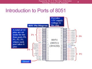
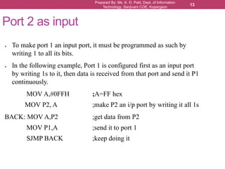
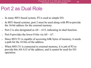
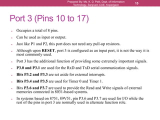
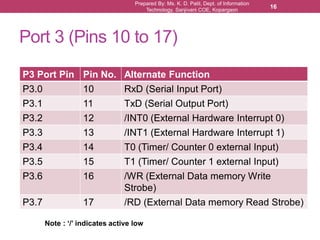
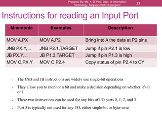
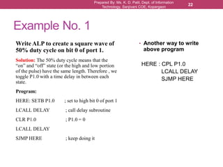
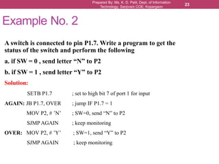
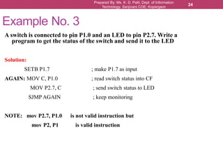
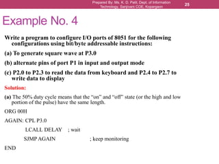
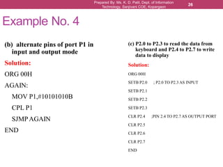
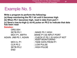
Unit 5: 8051 I/O Port Programming
Subject: Processor Architecture & Interfacing
(SPPU,Pune2015CourseofInformation Technology)
Class: SEIT Semester: II
Prepared By,
Ms. K. D. Patil, Assistant Professor
Department of Information Technology
(NBA accredited)
Sanjivani College of Engineering, Kopargaon-423603.
Maharashtra, India.
(An Autonomous Institute, Affiliated with SPPU, Pune.)
NAAC ‘A’ Grade Accredited, ISO 9001:2015 certified
Learning Outcomes
• Students will be able to
• Learn different ports of 8051
• Apply knowledge of 8051 assembly language to write a
code for 8051 I/O port programming
Prepared By: Ms. K. D. Patil, Dept. of Information
Technology, Sanjivani COE, Kopargaon
2
Contents
• Introduction to 8051 Ports
• Port 0
• Port 1
• Port 2
• Port3
• Different Ways of Accessing Entire Byte
• I/O Ports and Bit addressability
• Single Bit Instructions
• Examples
Prepared By: Ms. K. D. Patil, Dept. of Information
Technology, Sanjivani COE, Kopargaon
3
Introduction to Ports of 8051
Prepared By: Ms. K. D. Patil, Dept. of Information
Technology, Sanjivani COE, Kopargaon
4
Introduction to Ports of 8051
● As shown in the figure, In 8051 there are a total of
four ports for I/O operations.
● Out of 40 pins, a total of 32 pins are set aside for
the four ports P0,P1,P2 and P3, where each port
takes 8 pins.
● All ports upon RESET are configured as inputs,
when first 0 (zero) is written to port, it becomes
output.
● To reconfigure it as an input, 1 must be sent to the
port.
Prepared By: Ms. K. D. Patil, Dept. of Information
Technology, Sanjivani COE, Kopargaon
5
Prepared By: Ms. K. D. Patil, Dept. of Information
Technology, Sanjivani COE, Kopargaon
6
Port 0 (Pins 39 to 32 )
● A total of 8 pins.
● Can be used for Input or output.
● To use it as input or output,
each must be connected
externally to 10 k-ohm pull up
resistor.
● This is due to the fact that P0 is
an open drain, unlike P1, P2,
and P3.
● Open drain is a term used for
MOS chips in the same way
that open collector is used for
TTL chips.
Prepared By: Ms. K. D. Patil, Dept. of Information
Technology, Sanjivani COE, Kopargaon
7
Port 0
● The following code will continuously send out to port 0 the
alternating values of 55H and AAH. By sending 55H (0101 0101)
and AAH (1010 1010) to given port continuously we can toggle
(switch from one state to another state) the bits.
BACK: MOV A, #55H
MOV P0, A
ACALL DELAY
MOV A, #0AAH
MOV P0, A
ACALL DELAY
SJMP BACK
Prepared By: Ms. K. D. Patil, Dept. of Information
Technology, Sanjivani COE, Kopargaon
8
Port 0 as Input
● With resistors connected to port 0, In order to make port 0 an input, the
port must be programmed by writing 1 to all the bits.
● In the following example, Port 0 is configured first as an input port by
writing 1s to it, and then data is received from that port and sent to P1
MOV A,#0FFH ;A=FF hex
MOV P0, A ;make P0 an i/p port by writing it all 1s
BACK: MOV A,P0 ;get data from P0
MOV P1,A ;send it to port 1
SJMP BACK ;keep doing it
Prepared By: Ms. K. D. Patil, Dept. of Information
Technology, Sanjivani COE, Kopargaon
9
Port 0 as Dual Role
● Port 0 is also designated as AD0-AD7, allowing it to be used for
both address and data
● When connecting an 8051/31 to an external memory, port 0 provides
both address and data.
● The 8051 multiplexes address and data through port 0 to save the
pins.
Prepared By: Ms. K. D. Patil, Dept. of Information
Technology, Sanjivani COE, Kopargaon
10
Port 1 (Pins 1 to 8)
● Occupies a total of 8 pins.
● Can be used as input or output.
● In contrast to port 0, this port does not need any pull-up resistors since it
already has pull-up resistors internally.
● Upon RESET, port 1 is configured as an input port.
● The following code will continuously send out to port 1 the alternating
values of 55H and AAH. By sending 55H (0101 0101) and AAH (1010
1010) to given port continuously, we can toggle (switch from one state to
another state) the bits.
BACK: MOV A, #55H
MOV P1, A
ACALL DELAY
CPL A ; complement register A (A = 1010 1010 after executing instruction.)
SJMP BACK
Prepared By: Ms. K. D. Patil, Dept. of Information
Technology, Sanjivani COE, Kopargaon
11
● To make port 1 an input port, it must be programmed as such by writing 1 to all its
bits.
● In the following example, Port 1 is configured first as an input port by writing 1s
to it, then data is received from that port and saved in R7 and R5.
MOV A, # 0FFH ; A = FFH
MOV P1, A ;make p1 as input port by writing all 1s to it
MOV A, P1 ; get data from p1
MOV R7,A ; save data in R7 register
ACALL DELAY ; wait
MOV A, P1 ; get data from p1
MOV R6, A ; save data in R6 register
ACALL DELAY ;wait
MOV A, P1 ; get data from p1
MOV R6, A ; save data in R5 register
Port 1 as input
Prepared By: Ms. K. D. Patil, Dept. of Information
Technology, Sanjivani COE, Kopargaon
12
Port 2 (Pins 21 to 28)
● Occupies a total of 8 pins.
● Can be used as input or output.
● Just like P1, this port does not need any pull-up resistors since it already has pull-
up resistors internally.
● Upon RESET, port 2 is configured as an input port.
● The following code will continuously send out to port 1 the alternating values of
55H and AAH.
BACK: MOV A, #55H
MOV P2, A
ACALL DELAY
CPL A ; complement reg. A (A = 1010 1010 after executing instruction.)
SJMP BACK
Prepared By: Ms. K. D. Patil, Dept. of Information
Technology, Sanjivani COE, Kopargaon
13
Port 2 as input
● To make port 1 an input port, it must be programmed as such by
writing 1 to all its bits.
● In the following example, Port 1 is configured first as an input port
by writing 1s to it, then data is received from that port and send it P1
continuously.
MOV A,#0FFH ;A=FF hex
MOV P2, A ;make P2 an i/p port by writing it all 1s
BACK: MOV A,P2 ;get data from P2
MOV P1,A ;send it to port 1
SJMP BACK ;keep doing it
Prepared By: Ms. K. D. Patil, Dept. of Information
Technology, Sanjivani COE, Kopargaon
14
Port 2 as Dual Role
● In many 8051-based system, P2 is used as simple I/O.
● In 8031-based systems, port 2 must be used along with P0 to provide
the 16-bit address for the external memory.
● Port 2 is also designated as A8 – A15, indicating its dual function.
● Port 0 provides the lower 8 bits via A0 – A7.
● Since 8031/51 is capable of accessing 64K bytes of memory, it needs
a path for the 16 bits of the address.
● When 8051/31 is connected to external memory, it is job of P2 to
provide bits A8-A15 of the address, and it cannot be used for I/O
operation.
Port 3 (Pins 10 to 17)
● Occupies a total of 8 pins.
● Can be used as input or output.
● Just like P1 and P2, this port does not need any pull-up resistors.
● Although upon RESET, port 3 is configured as an input port, it is not the way it is
most commonly used.
● Port 3 has the additional function of providing some extremely important signals.
● P3.0 and P3.1 are used for the RxD and TxD serial communication signals.
● Bits P3.2 and P3.3 are set aside for external interrupts.
● Bits P3.4 and P3.5 are used for Timer 0 and Timer 1.
● Bits P3.6 and P3.7 are used to provide the Read and Write signals of external
memories connected in 8031-based systems.
● In systems based on 8751, 89V51, pin P3.6 and P3.7 are used for I/O while the
rest of the pins in port 3 are normally used in alternate function role.
Prepared By: Ms. K. D. Patil, Dept. of Information
Technology, Sanjivani COE, Kopargaon
15
Port 3 (Pins 10 to 17)
Prepared By: Ms. K. D. Patil, Dept. of Information
Technology, Sanjivani COE, Kopargaon
16
P3 Port Pin Pin No. Alternate Function
P3.0 10 RxD (Serial Input Port)
P3.1 11 TxD (Serial Output Port)
P3.2 12 /INT0 (External Hardware Interrupt 0)
P3.3 13 /INT1 (External Hardware Interrupt 1)
P3.4 14 T0 (Timer/ Counter 0 external Input)
P3.5 15 T1 (Timer/ Counter 1 external Input)
P3.6 16 /WR (External Data memory Write
Strobe)
P3.7 17 /RD (External Data memory Read Strobe)
Note : ‘/’ indicates active low
Prepared By: Ms. K. D. Patil, Dept. of Information
Technology, Sanjivani COE, Kopargaon
17
Different Ways of Accessing Entire
Byte (8 Bits)
● One way of accessing entire port
without using Accumulator (A)
BACK: MOV P0, #55H
ACALL DELAY
MOV P0, #0AAH
ACALL DELAY
SJMP BACK
● One more way to do same thing
MOV A, #55H
BACK: MOV P0, A
ACALL DELAY
CPLA
SJMP BACK
● The entire 8 bits of
Port 0 are accessed
BACK: MOV A, #55H
MOV P0, A
ACALL DELAY
MOV A, #0AAH
MOV P0, A
ACALL DELAY
SJMP BACK
Prepared By: Ms. K. D. Patil, Dept. of Information
Technology, Sanjivani COE, Kopargaon
18
I/O Ports and Bit Addressability
● Sometimes we need to access only 1
or 2 bits of the port instead of entire
8 bits.
● 8051 port have a capability to access
individual bits of the port without
altering the rest of the bits in that
port.
● When accessing a port in single bit
manner, we use the syntax, “SETB
X.Y”
– Where, X is the port number
(0,1,2,3)
– Y is the desired bit number from
0 to 7 for the data bits D0 to D7
● Example:
BACK : CPL P1.2
ACALL DELAY
SJMP BACK
Above code complements bit 2 of port 1
only. Other bits will be as it is
● The above example can be written
as
AGAIN: SETB P1.2
ACALL DALAY
CLR P1.2
ACALL DELAY
SJMP AGAIN
Prepared By: Ms. K. D. Patil, Dept. of Information
Technology, Sanjivani COE, Kopargaon
19
Single Bit Addressability of Ports
Prepared By: Ms. K. D. Patil, Dept. of Information
Technology, Sanjivani COE, Kopargaon
20
Single Bit Instructions
● Instructions that are used for single-bit operations
are as follows
Instruction Function
SETB bit Set the bit (bit = 1)
CLR bit Clear the bit (bit = 0)
CPL bit Complement the bit (bit = NOT bit)
JB bit, target Jump to target if bit = 1 (jump if bit)
JNB bit, target Jump to target if bit = 0 (jump if no bit)
JBC bit, target Jump to target if bit = 1, clear bit (jump
if bit, then clear)
Prepared By: Ms. K. D. Patil, Dept. of Information
Technology, Sanjivani COE, Kopargaon
21
Instructions for reading an Input Port
● The JNB and JB instructions are widely use single-bit operations
● They allow you to monitor a bit and make a decision depending on whether it’s 0
or 1
● These two instructions can be used for any bits of I/O ports 0, 1, 2, and 3
● Port 3 is typically not used for any I/O, either single-bit or byte-wise
Mnemonic Examples Description
MOV A,PX MOV A,P2 Bring into A the data at P2 pins
JNB PX.Y, .. JNB P2.1,TARGET Jump if pin P2.1 is low
JB PX.Y, .. JB P1.3,TARGET Jump if pin P1.3 is high
MOV C,PX.Y MOV C,P2.4 Copy status of pin P2.4 to CY
Example No. 1
Write ALP to create a square wave of
50% duty cycle on bit 0 of port 1.
Solution: The 50% duty cycle means that the
“on” and “off” state (or the high and low portion
of the pulse) have the same length. Therefore , we
toggle P1.0 with a time delay in between each
state.
Program:
HERE: SETB P1.0 ; set to high bit 0 of port 1
LCALL DELAY ; call delay subroutine
CLR P1.0 ; P1.0 = 0
LCALL DELAY
SJMP HERE ; keep doing it
• Another way to write
above program
HERE : CPL P1.0
LCALL DELAY
SJMP HERE
Prepared By: Ms. K. D. Patil, Dept. of Information
Technology, Sanjivani COE, Kopargaon
22
Prepared By: Ms. K. D. Patil, Dept. of Information
Technology, Sanjivani COE, Kopargaon
23
Example No. 2
A switch is connected to pin P1.7. Write a program to get the
status of the switch and perform the following
a. if SW = 0 , send letter “N” to P2
b. if SW = 1 , send letter “Y” to P2
Solution:
SETB P1.7 ; set to high bit 7 of port 1 for input
AGAIN: JB P1.7, OVER ; jump IF P1.7 = 1
MOV P2, # ’N’ ; SW=0, send “N” to P2
SJMP AGAIN ; keep monitoring
OVER: MOV P2, # ’Y’ ; SW=1, send “Y” to P2
SJMP AGAIN ; keep monitoring
Prepared By: Ms. K. D. Patil, Dept. of Information
Technology, Sanjivani COE, Kopargaon
24
Example No. 3
A switch is connected to pin P1.0 and an LED to pin P2.7. Write a
program to get the status of the switch and send it to the LED
Solution:
SETB P1.7 ; make P1.7 as input
AGAIN: MOV C, P1.0 ; read switch status into CF
MOV P2.7, C ; send switch status to LED
SJMP AGAIN ; keep monitoring
NOTE: mov P2.7, P1.0 is not valid instruction but
mov P2, P1 is valid instruction
Prepared By: Ms. K. D. Patil, Dept. of Information
Technology, Sanjivani COE, Kopargaon
25
Example No. 4
Write a program to configure I/O ports of 8051 for the following
configurations using bit/byte addressable instructions:
(a) To generate square wave at P3.0
(b) alternate pins of port P1 in input and output mode
(c) P2.0 to P2.3 to read the data from keyboard and P2.4 to P2.7 to
write data to display
Solution:
(a) The 50% duty cycle means that the “on” and “off” state (or the high and low
portion of the pulse) have the same length.
ORG 00H
AGAIN: CPL P3.0
LCALL DELAY ; wait
SJMP AGAIN ; keep monitoring
END
Prepared By: Ms. K. D. Patil, Dept. of Information
Technology, Sanjivani COE, Kopargaon
26
Example No. 4
(b) alternate pins of port P1 in
input and output mode
Solution:
ORG 00H
AGAIN:
MOV P1,#10101010B
CPL P1
SJMPAGAIN
END
(c) P2.0 to P2.3 to read the data from
keyboard and P2.4 to P2.7 to write
data to display
Solution:
ORG 00H
SETB P2.0 ; P2.0 TO P2.3 AS INPUT
SETB P2.1
SETB P2.2
SETB P2.3
CLR P2.4 ;PIN 2.4 TO P2.7 AS OUTPUT PORT
CLR P2.5
CLR P2.6
CLR P2.7
END
Example No. 5
Write a program to perform the following:
(a) Keep monitoring the P0.1 bit until it becomes high
(b) When P0.1 becomes high, read in data from port 1
(c) Send a low-to-high (L-to-H) pulse on P0.2 to indicate that data
has been read
Solution:
ORG 00H
SETB P0.1 ; MAKE P0.1 HIGH
MOV P1, #0FFH ;MAKE P1 AS INPUT PORT
AGAIN: JNB P0.1, AGAIN ; CHECK IF P0.1 IS HIGH,IF NOT
; KEEP MONITORING
MOV A, P1 ; TAKE DATA FROM P1
CLR P0.2 ; LOW PULSE
SETB P0.2 ; HIGH PULSE
END
Prepared By: Ms. K. D. Patil, Dept. of Information
Technology, Sanjivani COE, Kopargaon
27
Reference
• “The 8051 Microcontroller and Embedded Systems using
Assembly and C” , Muhammad Ali Mazidi, Janice Gillispie
Mazidi, Rolin D. McKinlay, Second Edition, Pearson
publication
Prepared By: Ms. K. D. Patil, Dept. of Information
Technology, Sanjivani COE, Kopargaon
28
Prepared By: Ms. K. D. Patil, Dept. of Information
Technology, Sanjivani COE, Kopargaon
29

SE PAI Unit 5_IO programming in 8051

  • 1.
    Unit 5: 8051I/O Port Programming Subject: Processor Architecture & Interfacing (SPPU,Pune2015CourseofInformation Technology) Class: SEIT Semester: II Prepared By, Ms. K. D. Patil, Assistant Professor Department of Information Technology (NBA accredited) Sanjivani College of Engineering, Kopargaon-423603. Maharashtra, India. (An Autonomous Institute, Affiliated with SPPU, Pune.) NAAC ‘A’ Grade Accredited, ISO 9001:2015 certified
  • 2.
    Learning Outcomes • Studentswill be able to • Learn different ports of 8051 • Apply knowledge of 8051 assembly language to write a code for 8051 I/O port programming Prepared By: Ms. K. D. Patil, Dept. of Information Technology, Sanjivani COE, Kopargaon 2
  • 3.
    Contents • Introduction to8051 Ports • Port 0 • Port 1 • Port 2 • Port3 • Different Ways of Accessing Entire Byte • I/O Ports and Bit addressability • Single Bit Instructions • Examples Prepared By: Ms. K. D. Patil, Dept. of Information Technology, Sanjivani COE, Kopargaon 3
  • 4.
    Introduction to Portsof 8051 Prepared By: Ms. K. D. Patil, Dept. of Information Technology, Sanjivani COE, Kopargaon 4
  • 5.
    Introduction to Portsof 8051 ● As shown in the figure, In 8051 there are a total of four ports for I/O operations. ● Out of 40 pins, a total of 32 pins are set aside for the four ports P0,P1,P2 and P3, where each port takes 8 pins. ● All ports upon RESET are configured as inputs, when first 0 (zero) is written to port, it becomes output. ● To reconfigure it as an input, 1 must be sent to the port. Prepared By: Ms. K. D. Patil, Dept. of Information Technology, Sanjivani COE, Kopargaon 5
  • 6.
    Prepared By: Ms.K. D. Patil, Dept. of Information Technology, Sanjivani COE, Kopargaon 6 Port 0 (Pins 39 to 32 ) ● A total of 8 pins. ● Can be used for Input or output. ● To use it as input or output, each must be connected externally to 10 k-ohm pull up resistor. ● This is due to the fact that P0 is an open drain, unlike P1, P2, and P3. ● Open drain is a term used for MOS chips in the same way that open collector is used for TTL chips.
  • 7.
    Prepared By: Ms.K. D. Patil, Dept. of Information Technology, Sanjivani COE, Kopargaon 7 Port 0 ● The following code will continuously send out to port 0 the alternating values of 55H and AAH. By sending 55H (0101 0101) and AAH (1010 1010) to given port continuously we can toggle (switch from one state to another state) the bits. BACK: MOV A, #55H MOV P0, A ACALL DELAY MOV A, #0AAH MOV P0, A ACALL DELAY SJMP BACK
  • 8.
    Prepared By: Ms.K. D. Patil, Dept. of Information Technology, Sanjivani COE, Kopargaon 8 Port 0 as Input ● With resistors connected to port 0, In order to make port 0 an input, the port must be programmed by writing 1 to all the bits. ● In the following example, Port 0 is configured first as an input port by writing 1s to it, and then data is received from that port and sent to P1 MOV A,#0FFH ;A=FF hex MOV P0, A ;make P0 an i/p port by writing it all 1s BACK: MOV A,P0 ;get data from P0 MOV P1,A ;send it to port 1 SJMP BACK ;keep doing it
  • 9.
    Prepared By: Ms.K. D. Patil, Dept. of Information Technology, Sanjivani COE, Kopargaon 9 Port 0 as Dual Role ● Port 0 is also designated as AD0-AD7, allowing it to be used for both address and data ● When connecting an 8051/31 to an external memory, port 0 provides both address and data. ● The 8051 multiplexes address and data through port 0 to save the pins.
  • 10.
    Prepared By: Ms.K. D. Patil, Dept. of Information Technology, Sanjivani COE, Kopargaon 10 Port 1 (Pins 1 to 8) ● Occupies a total of 8 pins. ● Can be used as input or output. ● In contrast to port 0, this port does not need any pull-up resistors since it already has pull-up resistors internally. ● Upon RESET, port 1 is configured as an input port. ● The following code will continuously send out to port 1 the alternating values of 55H and AAH. By sending 55H (0101 0101) and AAH (1010 1010) to given port continuously, we can toggle (switch from one state to another state) the bits. BACK: MOV A, #55H MOV P1, A ACALL DELAY CPL A ; complement register A (A = 1010 1010 after executing instruction.) SJMP BACK
  • 11.
    Prepared By: Ms.K. D. Patil, Dept. of Information Technology, Sanjivani COE, Kopargaon 11 ● To make port 1 an input port, it must be programmed as such by writing 1 to all its bits. ● In the following example, Port 1 is configured first as an input port by writing 1s to it, then data is received from that port and saved in R7 and R5. MOV A, # 0FFH ; A = FFH MOV P1, A ;make p1 as input port by writing all 1s to it MOV A, P1 ; get data from p1 MOV R7,A ; save data in R7 register ACALL DELAY ; wait MOV A, P1 ; get data from p1 MOV R6, A ; save data in R6 register ACALL DELAY ;wait MOV A, P1 ; get data from p1 MOV R6, A ; save data in R5 register Port 1 as input
  • 12.
    Prepared By: Ms.K. D. Patil, Dept. of Information Technology, Sanjivani COE, Kopargaon 12 Port 2 (Pins 21 to 28) ● Occupies a total of 8 pins. ● Can be used as input or output. ● Just like P1, this port does not need any pull-up resistors since it already has pull- up resistors internally. ● Upon RESET, port 2 is configured as an input port. ● The following code will continuously send out to port 1 the alternating values of 55H and AAH. BACK: MOV A, #55H MOV P2, A ACALL DELAY CPL A ; complement reg. A (A = 1010 1010 after executing instruction.) SJMP BACK
  • 13.
    Prepared By: Ms.K. D. Patil, Dept. of Information Technology, Sanjivani COE, Kopargaon 13 Port 2 as input ● To make port 1 an input port, it must be programmed as such by writing 1 to all its bits. ● In the following example, Port 1 is configured first as an input port by writing 1s to it, then data is received from that port and send it P1 continuously. MOV A,#0FFH ;A=FF hex MOV P2, A ;make P2 an i/p port by writing it all 1s BACK: MOV A,P2 ;get data from P2 MOV P1,A ;send it to port 1 SJMP BACK ;keep doing it
  • 14.
    Prepared By: Ms.K. D. Patil, Dept. of Information Technology, Sanjivani COE, Kopargaon 14 Port 2 as Dual Role ● In many 8051-based system, P2 is used as simple I/O. ● In 8031-based systems, port 2 must be used along with P0 to provide the 16-bit address for the external memory. ● Port 2 is also designated as A8 – A15, indicating its dual function. ● Port 0 provides the lower 8 bits via A0 – A7. ● Since 8031/51 is capable of accessing 64K bytes of memory, it needs a path for the 16 bits of the address. ● When 8051/31 is connected to external memory, it is job of P2 to provide bits A8-A15 of the address, and it cannot be used for I/O operation.
  • 15.
    Port 3 (Pins10 to 17) ● Occupies a total of 8 pins. ● Can be used as input or output. ● Just like P1 and P2, this port does not need any pull-up resistors. ● Although upon RESET, port 3 is configured as an input port, it is not the way it is most commonly used. ● Port 3 has the additional function of providing some extremely important signals. ● P3.0 and P3.1 are used for the RxD and TxD serial communication signals. ● Bits P3.2 and P3.3 are set aside for external interrupts. ● Bits P3.4 and P3.5 are used for Timer 0 and Timer 1. ● Bits P3.6 and P3.7 are used to provide the Read and Write signals of external memories connected in 8031-based systems. ● In systems based on 8751, 89V51, pin P3.6 and P3.7 are used for I/O while the rest of the pins in port 3 are normally used in alternate function role. Prepared By: Ms. K. D. Patil, Dept. of Information Technology, Sanjivani COE, Kopargaon 15
  • 16.
    Port 3 (Pins10 to 17) Prepared By: Ms. K. D. Patil, Dept. of Information Technology, Sanjivani COE, Kopargaon 16 P3 Port Pin Pin No. Alternate Function P3.0 10 RxD (Serial Input Port) P3.1 11 TxD (Serial Output Port) P3.2 12 /INT0 (External Hardware Interrupt 0) P3.3 13 /INT1 (External Hardware Interrupt 1) P3.4 14 T0 (Timer/ Counter 0 external Input) P3.5 15 T1 (Timer/ Counter 1 external Input) P3.6 16 /WR (External Data memory Write Strobe) P3.7 17 /RD (External Data memory Read Strobe) Note : ‘/’ indicates active low
  • 17.
    Prepared By: Ms.K. D. Patil, Dept. of Information Technology, Sanjivani COE, Kopargaon 17 Different Ways of Accessing Entire Byte (8 Bits) ● One way of accessing entire port without using Accumulator (A) BACK: MOV P0, #55H ACALL DELAY MOV P0, #0AAH ACALL DELAY SJMP BACK ● One more way to do same thing MOV A, #55H BACK: MOV P0, A ACALL DELAY CPLA SJMP BACK ● The entire 8 bits of Port 0 are accessed BACK: MOV A, #55H MOV P0, A ACALL DELAY MOV A, #0AAH MOV P0, A ACALL DELAY SJMP BACK
  • 18.
    Prepared By: Ms.K. D. Patil, Dept. of Information Technology, Sanjivani COE, Kopargaon 18 I/O Ports and Bit Addressability ● Sometimes we need to access only 1 or 2 bits of the port instead of entire 8 bits. ● 8051 port have a capability to access individual bits of the port without altering the rest of the bits in that port. ● When accessing a port in single bit manner, we use the syntax, “SETB X.Y” – Where, X is the port number (0,1,2,3) – Y is the desired bit number from 0 to 7 for the data bits D0 to D7 ● Example: BACK : CPL P1.2 ACALL DELAY SJMP BACK Above code complements bit 2 of port 1 only. Other bits will be as it is ● The above example can be written as AGAIN: SETB P1.2 ACALL DALAY CLR P1.2 ACALL DELAY SJMP AGAIN
  • 19.
    Prepared By: Ms.K. D. Patil, Dept. of Information Technology, Sanjivani COE, Kopargaon 19 Single Bit Addressability of Ports
  • 20.
    Prepared By: Ms.K. D. Patil, Dept. of Information Technology, Sanjivani COE, Kopargaon 20 Single Bit Instructions ● Instructions that are used for single-bit operations are as follows Instruction Function SETB bit Set the bit (bit = 1) CLR bit Clear the bit (bit = 0) CPL bit Complement the bit (bit = NOT bit) JB bit, target Jump to target if bit = 1 (jump if bit) JNB bit, target Jump to target if bit = 0 (jump if no bit) JBC bit, target Jump to target if bit = 1, clear bit (jump if bit, then clear)
  • 21.
    Prepared By: Ms.K. D. Patil, Dept. of Information Technology, Sanjivani COE, Kopargaon 21 Instructions for reading an Input Port ● The JNB and JB instructions are widely use single-bit operations ● They allow you to monitor a bit and make a decision depending on whether it’s 0 or 1 ● These two instructions can be used for any bits of I/O ports 0, 1, 2, and 3 ● Port 3 is typically not used for any I/O, either single-bit or byte-wise Mnemonic Examples Description MOV A,PX MOV A,P2 Bring into A the data at P2 pins JNB PX.Y, .. JNB P2.1,TARGET Jump if pin P2.1 is low JB PX.Y, .. JB P1.3,TARGET Jump if pin P1.3 is high MOV C,PX.Y MOV C,P2.4 Copy status of pin P2.4 to CY
  • 22.
    Example No. 1 WriteALP to create a square wave of 50% duty cycle on bit 0 of port 1. Solution: The 50% duty cycle means that the “on” and “off” state (or the high and low portion of the pulse) have the same length. Therefore , we toggle P1.0 with a time delay in between each state. Program: HERE: SETB P1.0 ; set to high bit 0 of port 1 LCALL DELAY ; call delay subroutine CLR P1.0 ; P1.0 = 0 LCALL DELAY SJMP HERE ; keep doing it • Another way to write above program HERE : CPL P1.0 LCALL DELAY SJMP HERE Prepared By: Ms. K. D. Patil, Dept. of Information Technology, Sanjivani COE, Kopargaon 22
  • 23.
    Prepared By: Ms.K. D. Patil, Dept. of Information Technology, Sanjivani COE, Kopargaon 23 Example No. 2 A switch is connected to pin P1.7. Write a program to get the status of the switch and perform the following a. if SW = 0 , send letter “N” to P2 b. if SW = 1 , send letter “Y” to P2 Solution: SETB P1.7 ; set to high bit 7 of port 1 for input AGAIN: JB P1.7, OVER ; jump IF P1.7 = 1 MOV P2, # ’N’ ; SW=0, send “N” to P2 SJMP AGAIN ; keep monitoring OVER: MOV P2, # ’Y’ ; SW=1, send “Y” to P2 SJMP AGAIN ; keep monitoring
  • 24.
    Prepared By: Ms.K. D. Patil, Dept. of Information Technology, Sanjivani COE, Kopargaon 24 Example No. 3 A switch is connected to pin P1.0 and an LED to pin P2.7. Write a program to get the status of the switch and send it to the LED Solution: SETB P1.7 ; make P1.7 as input AGAIN: MOV C, P1.0 ; read switch status into CF MOV P2.7, C ; send switch status to LED SJMP AGAIN ; keep monitoring NOTE: mov P2.7, P1.0 is not valid instruction but mov P2, P1 is valid instruction
  • 25.
    Prepared By: Ms.K. D. Patil, Dept. of Information Technology, Sanjivani COE, Kopargaon 25 Example No. 4 Write a program to configure I/O ports of 8051 for the following configurations using bit/byte addressable instructions: (a) To generate square wave at P3.0 (b) alternate pins of port P1 in input and output mode (c) P2.0 to P2.3 to read the data from keyboard and P2.4 to P2.7 to write data to display Solution: (a) The 50% duty cycle means that the “on” and “off” state (or the high and low portion of the pulse) have the same length. ORG 00H AGAIN: CPL P3.0 LCALL DELAY ; wait SJMP AGAIN ; keep monitoring END
  • 26.
    Prepared By: Ms.K. D. Patil, Dept. of Information Technology, Sanjivani COE, Kopargaon 26 Example No. 4 (b) alternate pins of port P1 in input and output mode Solution: ORG 00H AGAIN: MOV P1,#10101010B CPL P1 SJMPAGAIN END (c) P2.0 to P2.3 to read the data from keyboard and P2.4 to P2.7 to write data to display Solution: ORG 00H SETB P2.0 ; P2.0 TO P2.3 AS INPUT SETB P2.1 SETB P2.2 SETB P2.3 CLR P2.4 ;PIN 2.4 TO P2.7 AS OUTPUT PORT CLR P2.5 CLR P2.6 CLR P2.7 END
  • 27.
    Example No. 5 Writea program to perform the following: (a) Keep monitoring the P0.1 bit until it becomes high (b) When P0.1 becomes high, read in data from port 1 (c) Send a low-to-high (L-to-H) pulse on P0.2 to indicate that data has been read Solution: ORG 00H SETB P0.1 ; MAKE P0.1 HIGH MOV P1, #0FFH ;MAKE P1 AS INPUT PORT AGAIN: JNB P0.1, AGAIN ; CHECK IF P0.1 IS HIGH,IF NOT ; KEEP MONITORING MOV A, P1 ; TAKE DATA FROM P1 CLR P0.2 ; LOW PULSE SETB P0.2 ; HIGH PULSE END Prepared By: Ms. K. D. Patil, Dept. of Information Technology, Sanjivani COE, Kopargaon 27
  • 28.
    Reference • “The 8051Microcontroller and Embedded Systems using Assembly and C” , Muhammad Ali Mazidi, Janice Gillispie Mazidi, Rolin D. McKinlay, Second Edition, Pearson publication Prepared By: Ms. K. D. Patil, Dept. of Information Technology, Sanjivani COE, Kopargaon 28
  • 29.
    Prepared By: Ms.K. D. Patil, Dept. of Information Technology, Sanjivani COE, Kopargaon 29