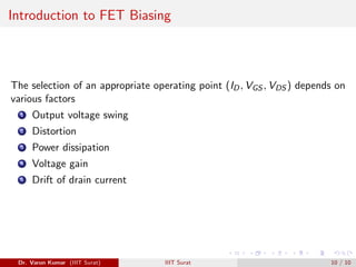
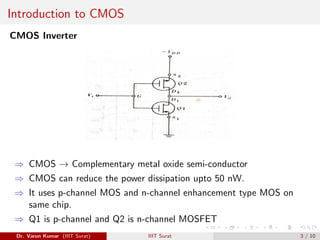
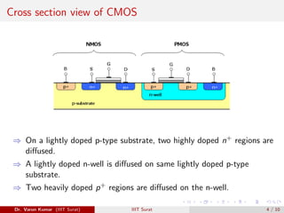
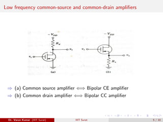
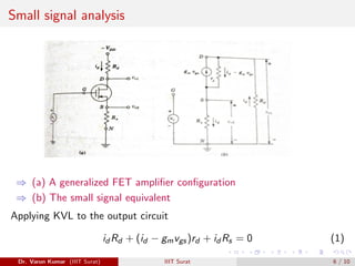
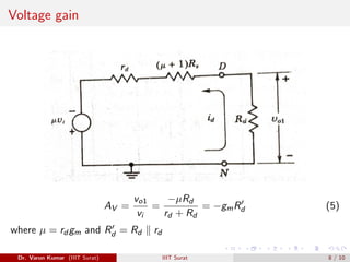
FET Amplifier and its Biasing
Dr. Varun Kumar
Dr. Varun Kumar (IIIT Surat) IIIT Surat 1 / 10
Outlines
1 Introduction to CMOS
2 Low Frequency Common Source and Common Drain Amplifier
3 Introduction to FET Biasing
Dr. Varun Kumar (IIIT Surat) IIIT Surat 2 / 10
Introduction to CMOS
CMOS Inverter
⇒ CMOS → Complementary metal oxide semi-conductor
⇒ CMOS can reduce the power dissipation upto 50 nW.
⇒ It uses p-channel MOS and n-channel enhancement type MOS on
same chip.
⇒ Q1 is p-channel and Q2 is n-channel MOSFET
Dr. Varun Kumar (IIIT Surat) IIIT Surat 3 / 10
Cross section view of CMOS
⇒ On a lightly doped p-type substrate, two highly doped n+ regions are
diffused.
⇒ A lightly doped n-well is diffused on same lightly doped p-type
substrate.
⇒ Two heavily doped p+ regions are diffused on the n-well.
Dr. Varun Kumar (IIIT Surat) IIIT Surat 4 / 10
Low frequency common-source and common-drain amplifiers
⇒ (a) Common source amplifier ⇐⇒ Bipolar CE amplifier
⇒ (b) Common drain amplifier ⇐⇒ Bipolar CC amplifier
Dr. Varun Kumar (IIIT Surat) IIIT Surat 5 / 10
Small signal analysis
⇒ (a) A generalized FET amplifier configuration
⇒ (b) The small signal equivalent
Applying KVL to the output circuit
id Rd + (id − gmvgs)rd + id Rs = 0 (1)
Dr. Varun Kumar (IIIT Surat) IIIT Surat 6 / 10
Continued–
From above figure,
vgs = vi − id Rs (2)
Combining (1) and (2) and remembering that µ = rd gm, we find that
id =
µvi
rd + Rd + (µ + 1)Rs
(3)
CS Amplifier with an Unbypassed Source Resistance
Since vo1 = −id Rd then
vo1 =
−µvi Rd
rd + Rd + (µ + 1)Rs
(4)
From (4), the open circuit voltage is −µvi and output resistance is
R0 = rd + (µ + 1)Rs
Dr. Varun Kumar (IIIT Surat) IIIT Surat 7 / 10
Voltage gain
AV =
vo1
vi
=
−µRd
rd + Rd
= −gmR0
d (5)
where µ = rd gm and R0
d = Rd k rd
Dr. Varun Kumar (IIIT Surat) IIIT Surat 8 / 10
CD Amplifier with a Drain Resistance
Since vo2 = id Rs, then from (3)
vo2 =
µvi Rs
rd + Rd + (µ + 1)Rs
=
[µvi /(µ + 1)]Rs
(rd + Rd )/(µ + 1) + Rs
(6)
In CD amplifier, the open circuited voltage is µvi
(µ+1) and output resistance
is Ro = Rd +rd
(µ+1) and voltage gain AV = vo2
vi
Dr. Varun Kumar (IIIT Surat) IIIT Surat 9 / 10
Introduction to FET Biasing
The selection of an appropriate operating point (ID, VGS , VDS ) depends on
various factors
1 Output voltage swing
2 Distortion
3 Power dissipation
4 Voltage gain
5 Drift of drain current
Dr. Varun Kumar (IIIT Surat) IIIT Surat 10 / 10

CMOS, FET Amplifier

  • 1.
    FET Amplifier andits Biasing Dr. Varun Kumar Dr. Varun Kumar (IIIT Surat) IIIT Surat 1 / 10
  • 2.
    Outlines 1 Introduction toCMOS 2 Low Frequency Common Source and Common Drain Amplifier 3 Introduction to FET Biasing Dr. Varun Kumar (IIIT Surat) IIIT Surat 2 / 10
  • 3.
    Introduction to CMOS CMOSInverter ⇒ CMOS → Complementary metal oxide semi-conductor ⇒ CMOS can reduce the power dissipation upto 50 nW. ⇒ It uses p-channel MOS and n-channel enhancement type MOS on same chip. ⇒ Q1 is p-channel and Q2 is n-channel MOSFET Dr. Varun Kumar (IIIT Surat) IIIT Surat 3 / 10
  • 4.
    Cross section viewof CMOS ⇒ On a lightly doped p-type substrate, two highly doped n+ regions are diffused. ⇒ A lightly doped n-well is diffused on same lightly doped p-type substrate. ⇒ Two heavily doped p+ regions are diffused on the n-well. Dr. Varun Kumar (IIIT Surat) IIIT Surat 4 / 10
  • 5.
    Low frequency common-sourceand common-drain amplifiers ⇒ (a) Common source amplifier ⇐⇒ Bipolar CE amplifier ⇒ (b) Common drain amplifier ⇐⇒ Bipolar CC amplifier Dr. Varun Kumar (IIIT Surat) IIIT Surat 5 / 10
  • 6.
    Small signal analysis ⇒(a) A generalized FET amplifier configuration ⇒ (b) The small signal equivalent Applying KVL to the output circuit id Rd + (id − gmvgs)rd + id Rs = 0 (1) Dr. Varun Kumar (IIIT Surat) IIIT Surat 6 / 10
  • 7.
    Continued– From above figure, vgs= vi − id Rs (2) Combining (1) and (2) and remembering that µ = rd gm, we find that id = µvi rd + Rd + (µ + 1)Rs (3) CS Amplifier with an Unbypassed Source Resistance Since vo1 = −id Rd then vo1 = −µvi Rd rd + Rd + (µ + 1)Rs (4) From (4), the open circuit voltage is −µvi and output resistance is R0 = rd + (µ + 1)Rs Dr. Varun Kumar (IIIT Surat) IIIT Surat 7 / 10
  • 8.
    Voltage gain AV = vo1 vi = −µRd rd+ Rd = −gmR0 d (5) where µ = rd gm and R0 d = Rd k rd Dr. Varun Kumar (IIIT Surat) IIIT Surat 8 / 10
  • 9.
    CD Amplifier witha Drain Resistance Since vo2 = id Rs, then from (3) vo2 = µvi Rs rd + Rd + (µ + 1)Rs = [µvi /(µ + 1)]Rs (rd + Rd )/(µ + 1) + Rs (6) In CD amplifier, the open circuited voltage is µvi (µ+1) and output resistance is Ro = Rd +rd (µ+1) and voltage gain AV = vo2 vi Dr. Varun Kumar (IIIT Surat) IIIT Surat 9 / 10
  • 10.
    Introduction to FETBiasing The selection of an appropriate operating point (ID, VGS , VDS ) depends on various factors 1 Output voltage swing 2 Distortion 3 Power dissipation 4 Voltage gain 5 Drift of drain current Dr. Varun Kumar (IIIT Surat) IIIT Surat 10 / 10