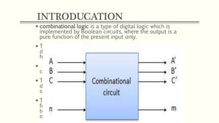
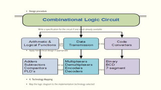
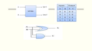
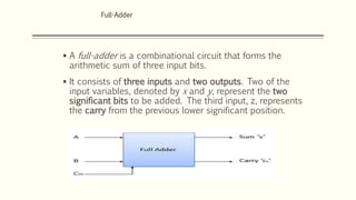
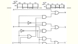
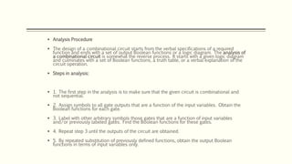
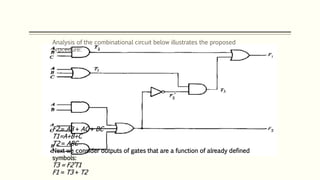
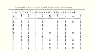
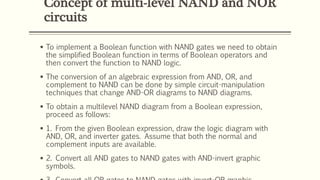
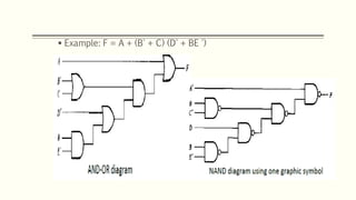
Er. Nawaraj Bhandari
Digital Logic
Chapter 4: COMBINATIONAL LOGIC
INTRODUCATION
 combinational logic is a type of digital logic which is
implemented by Boolean circuits, where the output is a
pure function of the present input only.
 This is in contrast to sequential logic, in which the output
depends not only on the present input but also on the
history of the input.
 In other words, sequential logic has memory while
combinational logic does not.
 The outputs of Combinational Logic Circuits are only
determined by the logical function of their current input
state, logic “0” or logic “1”, at any given instant in time.
 The result is that combinational logic circuits have no
feedback, and any changes to the signals being applied
to their inputs will immediately have an effect at the
output
 Design procedure
 The design of combinational circuits starts from the verbal outline of the problem and ends in a logic
circuit diagram or a set of Boolean functions from which the logic diagram can be easily obtained. The
procedure involves the following steps:
 1. Specification
Write a specification for the circuit if one is not already available
 2. Formulation
 Derive a truth table or initial Boolean equations that define the required relationships between the inputs
and outputs, if not in the specification.
 Apply hierarchical design if appropriate
 3. Optimization
 Apply 2-level and multiple-level optimization
 Draw a logic diagram for the resulting circuit using ANDs, ORs, and inverters
 4. Technology Mapping
 Map the logic diagram to the implementation technology selected
Adder
 Digital computers perform a variety of information-processing
tasks. Among the basic functions encountered are the various
arithmetic operations.
 The most basic arithmetic operation, no doubt, is the addition
of two binary digits.
 Half-Adder
 A combinational circuit that performs the addition of two bits is
called a half-adder.
 Circuit needs two inputs and two outputs. The input variables
designate the augend (x) and addend (y) bits; the output
variables produce the sum (S) and carry (C).
 In half adder we do not add carry from previous one.
 It is the basic building block for addition of two single bit
numbers.
 A full-adder is a combinational circuit that forms the
arithmetic sum of three input bits.
 It consists of three inputs and two outputs. Two of the
input variables, denoted by x and y, represent the two
significant bits to be added. The third input, z, represents
the carry from the previous lower significant position.
Full-Adder
1 1
1 1
K-MAP For
S=A’B’C+A’BC’+AB’C’+ABC
1
1 1 1
K-MAP For C0=AB+AC+BC
IMPLIMENTATION OF FULL ADDER
WITH TWO HALF ADDER
 We can achieve a full adder using two half adder.
 We have to take two half adder in one sequence and lets
assume S1,c1 is the sum and carry of first adder and
S2,c2 is the sum and carry of second adder.
 So for the second adder S1 is the input and and also Cin
is the work as input for second
Substractor
 The subtraction of two binary numbers may be
accomplished by taking the complement of the
subtrahend and adding it to the minuend.
 By this method, the subtraction operation becomes an
addition operation requiring full-adders for its machine
implementation.
 It is possible to implement subtraction with logic circuits
in a direct manner, as done with paper and pencil.
 By this method, each subtrahend bit of the number is
subtracted from its corresponding significant minuend bit
to form a difference bit.
 If the minuend bit is smaller than the subtrahend bit, a 1
is borrowed from the next significant position
Half-Subtractor
 A half-subtractor is a combinational circuit that subtracts two
bits and produces their difference bit.
 Denoting minuend bit by x and the subtrahend bit by y.
 To perform x - y, we have to check the relative magnitudes of x
and y:
 If x≥ y, we have three possibilities: 0 - 0 = 0, 1 - 0 = 1, and 1 -
1 = 0.
 If x < y, we have 0 - 1, and it is necessary to borrow a 1 from
the next higher stage.
 The half-subtractor needs two outputs, difference (D) and
borrow (B).
 D = A‘B + AB‘ B0= A‘B
Half sub
diff
‘D’
barrow‘B0’
D
B00
0
1
1
1
0
0
0
D
B0
FULL SUBTRACTOR
 Full-Subtractor
 A full-subtractor is a combinational circuit that performs a
subtraction between two bits, taking into account that a 1
may have been borrowed by a lower significant stage.
 This circuit has three inputs and two outputs. The three
inputs, x, y, and z, denote the minuend, subtrahend, and
previous borrow, respectively.
 The two outputs, D and B, represent the difference and
output-borrow, respectively.
D = x'y'z + x'yz' + xy'z' + xyz B = x'y + x'z + yz
Code Conversion
 The availability of a large variety of codes for the same discrete
elements of information results in the use of different codes by
different digital systems. It is sometimes necessary to use the output
of one system as the input to another.
 A conversion circuit must be inserted between the two systems if
each uses different codes for the same information.
 Thus, a code converter is a circuit that makes the two systems
compatible even though each uses a different binary code.
 To convert from binary code A to binary code B, code converter has
input lines supplying the bit combination of elements as specified by
code A and the output lines of the converter generating the
corresponding bit combination of code B.
 A Code converter (combinational circuit) performs this
transformation by means of logic gates.
 The design procedure of code converters will be illustrated by
means of a specific example of conversion from the BCD to the
excess-3 code.
BCD to Excess-3 code converter
 Transforms BCD code for the decimal digits to Excess-3 code
for the decimal digits
 BCD code words for digits 0 through 9: 4-bit patterns 0000 to
1001, respectively.
 Excess-3 code words for digits 0 through 9: 4-bit patterns
consisting of 3 (binary 0011) added to each BCD code word
 Implementation: multiple-level circuit
 Conversion of 4-bit codes can be most easily formulated by a
truth table
 Variables- BCD: A, B, C, D
 Variables- Excess-3: W, X, Y, Z
 Don’t Cares: BCD 1010 to 1111
 Analysis Procedure
 The design of a combinational circuit starts from the verbal specifications of a required
function and ends with a set of output Boolean functions or a logic diagram. The analysis of
a combinational circuit is somewhat the reverse process. It starts with a given logic diagram
and culminates with a set of Boolean functions, a truth table, or a verbal explanation of the
circuit operation.
 Steps in analysis:
 1. The first step in the analysis is to make sure that the given circuit is combinational and
not sequential.
 2. Assign symbols to all gate outputs that are a function of the input variables. Obtain the
Boolean functions for each gate.
 3. Label with other arbitrary symbols those gates that are a function of input variables
and/or previously labeled gates. Find the Boolean functions for these gates.
 4. Repeat step 3 until the outputs of the circuit are obtained.
 5. By repeated substitution of previously defined functions, obtain the output Boolean
functions in terms of input variables only.
F2 = AB + AC + BC
T1=A+B+C
T2 = ABC
Next we consider outputs of gates that are a function of already defined
symbols:
T3 = F2’T1
F1 = T3 + T2
Analysis of the combinational circuit below illustrates the proposed
procedure:
To obtain F1 as a function of A, B, and C, forms a series of substitutions
as follows:
If you want to determine the information-transformation task
achieved by this circuit, you can derive the truth table directly
from the Boolean functions and try to recognize a familiar
operation. For this example, we note that the circuit is a full-
adder, with F, being the sum output and F, the carry output. A,
B, and C are the three inputs added arithmetically.
Concept of multi-level NAND and NOR
circuits
 To implement a Boolean function with NAND gates we need to obtain
the simplified Boolean function in terms of Boolean operators and
then convert the function to NAND logic.
 The conversion of an algebraic expression from AND, OR, and
complement to NAND can be done by simple circuit-manipulation
techniques that change AND-OR diagrams to NAND diagrams.
 To obtain a multilevel NAND diagram from a Boolean expression,
proceed as follows:
 1. From the given Boolean expression, draw the logic diagram with
AND, OR, and inverter gates. Assume that both the normal and
complement inputs are available.
 2. Convert all AND gates to NAND gates with AND-invert graphic
symbols.
 Example: F = A + (B' + C) (D' + BE ')
 Multi-level NOR circuits
 The NOR function is the dual of the NAND function.
 For this reason, all procedures and rules for NOR logic form a dual of the
corresponding procedures and rules developed for NAND logic.
 Similar to NAND, NOR has also two graphic symbols: OR-invert and invert-AND
symbol.
 The procedure for implementing a Boolean function with NOR gates is similar to
the procedure outlined in the previous section for NAND gates:
 1. Draw the AND-OR logic diagram from the given algebraic expression. Assume
that both the normal and complement inputs are available.
 2. Convert all OR gates to NOR gates with OR-invert graphic symbols.
 3. Convert all AND gates to NOR gates with invert-AND graphic symbols.
 4. Any small circle that is not compensated by another small circle along the
same line needs an inverter or the complementation of the input variable.
Example: F = (AB + E) (C + D)

Chapter 4: Combinational Logic

  • 1.
    Er. Nawaraj Bhandari DigitalLogic Chapter 4: COMBINATIONAL LOGIC
  • 2.
    INTRODUCATION  combinational logicis a type of digital logic which is implemented by Boolean circuits, where the output is a pure function of the present input only.  This is in contrast to sequential logic, in which the output depends not only on the present input but also on the history of the input.  In other words, sequential logic has memory while combinational logic does not.  The outputs of Combinational Logic Circuits are only determined by the logical function of their current input state, logic “0” or logic “1”, at any given instant in time.  The result is that combinational logic circuits have no feedback, and any changes to the signals being applied to their inputs will immediately have an effect at the output
  • 3.
     Design procedure The design of combinational circuits starts from the verbal outline of the problem and ends in a logic circuit diagram or a set of Boolean functions from which the logic diagram can be easily obtained. The procedure involves the following steps:  1. Specification Write a specification for the circuit if one is not already available  2. Formulation  Derive a truth table or initial Boolean equations that define the required relationships between the inputs and outputs, if not in the specification.  Apply hierarchical design if appropriate  3. Optimization  Apply 2-level and multiple-level optimization  Draw a logic diagram for the resulting circuit using ANDs, ORs, and inverters  4. Technology Mapping  Map the logic diagram to the implementation technology selected
  • 4.
    Adder  Digital computersperform a variety of information-processing tasks. Among the basic functions encountered are the various arithmetic operations.  The most basic arithmetic operation, no doubt, is the addition of two binary digits.  Half-Adder  A combinational circuit that performs the addition of two bits is called a half-adder.  Circuit needs two inputs and two outputs. The input variables designate the augend (x) and addend (y) bits; the output variables produce the sum (S) and carry (C).  In half adder we do not add carry from previous one.  It is the basic building block for addition of two single bit numbers.
  • 6.
     A full-adderis a combinational circuit that forms the arithmetic sum of three input bits.  It consists of three inputs and two outputs. Two of the input variables, denoted by x and y, represent the two significant bits to be added. The third input, z, represents the carry from the previous lower significant position. Full-Adder
  • 7.
    1 1 1 1 K-MAPFor S=A’B’C+A’BC’+AB’C’+ABC 1 1 1 1 K-MAP For C0=AB+AC+BC
  • 8.
    IMPLIMENTATION OF FULLADDER WITH TWO HALF ADDER  We can achieve a full adder using two half adder.  We have to take two half adder in one sequence and lets assume S1,c1 is the sum and carry of first adder and S2,c2 is the sum and carry of second adder.  So for the second adder S1 is the input and and also Cin is the work as input for second
  • 9.
    Substractor  The subtractionof two binary numbers may be accomplished by taking the complement of the subtrahend and adding it to the minuend.  By this method, the subtraction operation becomes an addition operation requiring full-adders for its machine implementation.  It is possible to implement subtraction with logic circuits in a direct manner, as done with paper and pencil.  By this method, each subtrahend bit of the number is subtracted from its corresponding significant minuend bit to form a difference bit.  If the minuend bit is smaller than the subtrahend bit, a 1 is borrowed from the next significant position
  • 10.
    Half-Subtractor  A half-subtractoris a combinational circuit that subtracts two bits and produces their difference bit.  Denoting minuend bit by x and the subtrahend bit by y.  To perform x - y, we have to check the relative magnitudes of x and y:  If x≥ y, we have three possibilities: 0 - 0 = 0, 1 - 0 = 1, and 1 - 1 = 0.  If x < y, we have 0 - 1, and it is necessary to borrow a 1 from the next higher stage.  The half-subtractor needs two outputs, difference (D) and borrow (B).
  • 11.
     D =A‘B + AB‘ B0= A‘B Half sub diff ‘D’ barrow‘B0’ D B00 0 1 1 1 0 0 0 D B0
  • 12.
    FULL SUBTRACTOR  Full-Subtractor A full-subtractor is a combinational circuit that performs a subtraction between two bits, taking into account that a 1 may have been borrowed by a lower significant stage.  This circuit has three inputs and two outputs. The three inputs, x, y, and z, denote the minuend, subtrahend, and previous borrow, respectively.  The two outputs, D and B, represent the difference and output-borrow, respectively. D = x'y'z + x'yz' + xy'z' + xyz B = x'y + x'z + yz
  • 13.
    Code Conversion  Theavailability of a large variety of codes for the same discrete elements of information results in the use of different codes by different digital systems. It is sometimes necessary to use the output of one system as the input to another.  A conversion circuit must be inserted between the two systems if each uses different codes for the same information.  Thus, a code converter is a circuit that makes the two systems compatible even though each uses a different binary code.  To convert from binary code A to binary code B, code converter has input lines supplying the bit combination of elements as specified by code A and the output lines of the converter generating the corresponding bit combination of code B.  A Code converter (combinational circuit) performs this transformation by means of logic gates.  The design procedure of code converters will be illustrated by means of a specific example of conversion from the BCD to the excess-3 code.
  • 14.
    BCD to Excess-3code converter  Transforms BCD code for the decimal digits to Excess-3 code for the decimal digits  BCD code words for digits 0 through 9: 4-bit patterns 0000 to 1001, respectively.  Excess-3 code words for digits 0 through 9: 4-bit patterns consisting of 3 (binary 0011) added to each BCD code word  Implementation: multiple-level circuit  Conversion of 4-bit codes can be most easily formulated by a truth table  Variables- BCD: A, B, C, D  Variables- Excess-3: W, X, Y, Z  Don’t Cares: BCD 1010 to 1111
  • 16.
     Analysis Procedure The design of a combinational circuit starts from the verbal specifications of a required function and ends with a set of output Boolean functions or a logic diagram. The analysis of a combinational circuit is somewhat the reverse process. It starts with a given logic diagram and culminates with a set of Boolean functions, a truth table, or a verbal explanation of the circuit operation.  Steps in analysis:  1. The first step in the analysis is to make sure that the given circuit is combinational and not sequential.  2. Assign symbols to all gate outputs that are a function of the input variables. Obtain the Boolean functions for each gate.  3. Label with other arbitrary symbols those gates that are a function of input variables and/or previously labeled gates. Find the Boolean functions for these gates.  4. Repeat step 3 until the outputs of the circuit are obtained.  5. By repeated substitution of previously defined functions, obtain the output Boolean functions in terms of input variables only.
  • 17.
    F2 = AB+ AC + BC T1=A+B+C T2 = ABC Next we consider outputs of gates that are a function of already defined symbols: T3 = F2’T1 F1 = T3 + T2 Analysis of the combinational circuit below illustrates the proposed procedure:
  • 18.
    To obtain F1as a function of A, B, and C, forms a series of substitutions as follows: If you want to determine the information-transformation task achieved by this circuit, you can derive the truth table directly from the Boolean functions and try to recognize a familiar operation. For this example, we note that the circuit is a full- adder, with F, being the sum output and F, the carry output. A, B, and C are the three inputs added arithmetically.
  • 19.
    Concept of multi-levelNAND and NOR circuits  To implement a Boolean function with NAND gates we need to obtain the simplified Boolean function in terms of Boolean operators and then convert the function to NAND logic.  The conversion of an algebraic expression from AND, OR, and complement to NAND can be done by simple circuit-manipulation techniques that change AND-OR diagrams to NAND diagrams.  To obtain a multilevel NAND diagram from a Boolean expression, proceed as follows:  1. From the given Boolean expression, draw the logic diagram with AND, OR, and inverter gates. Assume that both the normal and complement inputs are available.  2. Convert all AND gates to NAND gates with AND-invert graphic symbols.
  • 20.
     Example: F= A + (B' + C) (D' + BE ')
  • 21.
     Multi-level NORcircuits  The NOR function is the dual of the NAND function.  For this reason, all procedures and rules for NOR logic form a dual of the corresponding procedures and rules developed for NAND logic.  Similar to NAND, NOR has also two graphic symbols: OR-invert and invert-AND symbol.  The procedure for implementing a Boolean function with NOR gates is similar to the procedure outlined in the previous section for NAND gates:  1. Draw the AND-OR logic diagram from the given algebraic expression. Assume that both the normal and complement inputs are available.  2. Convert all OR gates to NOR gates with OR-invert graphic symbols.  3. Convert all AND gates to NOR gates with invert-AND graphic symbols.  4. Any small circle that is not compensated by another small circle along the same line needs an inverter or the complementation of the input variable. Example: F = (AB + E) (C + D)