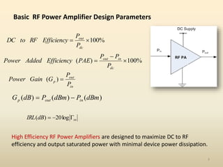
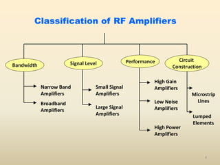
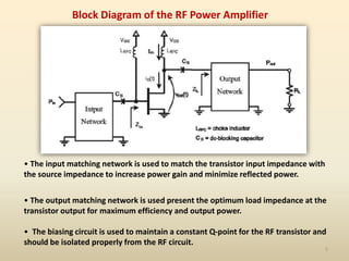
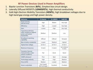
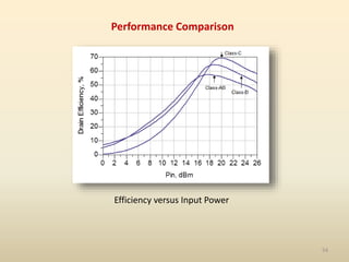
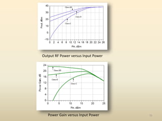
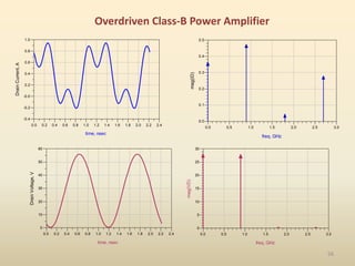
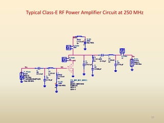
High Efficiency RF Power Amplifiers for
Mobile Transmitters
Firas Mohammed Ali, PhD
University of Technology, Iraq
E-mail: firas.m.ali@uotechnology.edu.iq
1
• The RF power amplifier is the final stage of a solid-state radio transmitter.
• The efficiency of the whole transmitter depends on the efficiency of the power
amplifier as it is the most power-hungry stage in the radio system.
• The battery size and life of the transmitter depends, to a large extent, on the
efficiency of the power amplifier.
Introduction
Block Diagram of a Typical Modern SDR Transmitter
2
Basic RF Power Amplifier Design Parameters
%
100


dc
out
P
P
Efficiency
RF
to
DC
%
100
)
( 


dc
in
out
P
P
P
PAE
Efficiency
Added
Power
in
out
p
P
P
G
Gain
Power 
)
(
)
(
)
(
)
( dBm
P
dBm
P
dB
G in
out
p 

High Efficiency RF Power Amplifiers are designed to maximize DC to RF
efficiency and output saturated power with minimal device power dissipation.
in
dB
IRL 

 log
20
)
(
3
Classification of RF Amplifiers
Bandwidth
Narrow Band
Amplifiers
Broadband
Amplifiers
Signal Level
Small Signal
Amplifiers
Large Signal
Amplifiers
Performance
High Gain
Amplifiers
Low Noise
Amplifiers
High Power
Amplifiers
Circuit
Construction
Microstrip
Lines
Lumped
Elements
4
Block Diagram of the RF Power Amplifier
• The input matching network is used to match the transistor input impedance with
the source impedance to increase power gain and minimize reflected power.
• The output matching network is used present the optimum load impedance at the
transistor output for maximum efficiency and output power.
• The biasing circuit is used to maintain a constant Q-point for the RF transistor and
should be isolated properly from the RF circuit.
5
Differences between Small Signal and Large Signal Power
Amplifiers
Small-Signal RF Transistor
Characterization
Small Signal
S-Parameters
Linear Circuit
Model
Ease of Measurements
High Accuracy of Modeling
Useful in Frequency
Domain Simulation
Difficulty of
Parameter
Measurements
Lower Accuracy
Useful in Time
Domain
Simulation
6
Large Signal RF Transistor
Characterization
Large-Signal
S-Parameters
(Parameters vary with
signal power level as well
as with frequency)
Load/Source Pull
Measurement
(Determination of
optimum load and source
impedances using
input/output tuners)
Non-linear Large
Signal Circuit Model
(Contains nonlinear
elements whose
values depend on
voltage levels)
7
8
Load Pull Measurements
• Small Signal RF Amplifiers operate on a small linear portion of the transistor
characteristic, while Power Amplifiers operate on large and usually nonlinear
portion of the transistor characteristic.
• Small signal high-gain RF amplifiers are usually designed for simultaneous
conjugate matching at input and output ports.
9
• In order to obtain maximum output power, typically the power amplifier is
not conjugately matched. Instead, the load network is designed such that the
amplifier has the correct voltage and current at the transistor output to
deliver the required power.
Power Amplifier Matching
Considerations
Comparison between maximum gain matching
and maximum output power matching
10
RF Power Devices Used in Power Amplifiers
1. Bipolar Junction Transistors (BJTs), Simplest bias circuit design.
2. Laterally Diffused MOSFETs (LDMOSFETs), high thermal conductivity.
3. GaN High-Electron Mobility Transistors (HEMTs), high breakdown voltages due to
high band-gap energy and high power density.
11
GaN RF Power Transistor Structure
12
Features
1. High Breakdown Voltages due to High Band-gap Energy.
2. High Power Density.
3. High Thermal Conductivity.
4. Low output parasitic capacitance.
13
Small-Signal Equivalent Circuit for HEMT
HEMT Large Signal Model
14
Classification of RF Power Amplifiers
Conventional
Mode
Switching
Mode
Harmonically
Tuned
Class A
Class B
Class AB
Class C
Class D Class E Class F Class F-1 Class J
• In conventional mode power amplifiers, the transistor is operating as a
current source.
• In switching mode power amplifiers, the transistor is operating as a switch.
• In harmonic-tuned power amplifiers the transistor is operating as a possibly
saturated (or over-driven) current source.
15
Continuous
Class F
Continuous
Class F-1
Vcc
0
2Vcc
0  2
t
i v
t
I
Icq
V
R
Vcc
0
i
vin
vin
Vin
Vb
t
i
 2
Vp
v
Class A
- input cosine voltage
t
V
V
v 
cos
in
b
in 

t
I
I
i cos
cq 


t
V
V
v 
cos
cc 

cc
cq
dc V
I
P 
IV
Pout 0.5



2
1
2
1
cq
cc
cq
dc I
I
V
V
I
I
P
Pout



cc
/V
V


1
/ cq 
I
I
.5
0


- output cosine current
- -DC output power
- fundamental output
power
Transfer characteristic
Input voltage
Output current
Output voltage
- collector efficiency
- voltage peak factor
For ideal condition of zero
saturation voltage when 1


- maximum collector efficiency in Class A
16
Vcc
 2
0
2Vcc
c
t
i v
t
V
R
Vcc
0
i
vin
vin
Vin
t
0  2
I
i
i1
 = 90



















2
,
0
,
cos
cq
t
t
t
I
I
i

cos
0 cq I
I
i 


I
Icq
cos 


 

 cos
cos 
 t
I
i
 

cos
1
max 

 I
I
i
- output current
conduction angle 2
indicates its duty cycle
- input cosine voltage
t
V
V
v 
cos
in
b
in 

For moment with zero current
For moment with maximum current
Class B
Transfer characteristic
Output voltage
Output current
Input voltage
17
Class-A,-B,-AB, -C operation modes
- quiescent current as function of half-conduction angle 
where

cos
cq I
I 

• when  > 90  cos  < 0  Icq > 0 - Class AB operation mode
• when  = 90  cos  = 0  Icq = 0 - Class B operation mode
• when  < 90  cos  > 0  Icq < 0 - Class C operation mode

3
cos
2
cos
cos 3
2
1
0 



 t
I
t
I
t
I
I
i 


  0
0 cos
cos
2
1







I
t
d
t
I
I 

 

  1
1 cos
cos
cos
1








I
t
d
t
t
I
I 

 

 ,
cos
sin
1
0 



 
  




 cos
sin
1
1 






2
1
2
1
0
1
0
1
0
1



I
I
P
P
1


When  = 90 and .785
0
4




- Fourier series
where - dc component
- fundamental component
- collector efficiency
- maximum collector
efficiency in Class B
- current
coefficients
18
t
0
i
v
t

Imax
i
 = 90
K
0
L
M P
Vcc 2Vcc
Imax
For increased input voltage
amplitude:
Output current
Input voltage
Transfer characteristic
Over-driven class-B RF Power Amplifier
MP – cut-off region
• operation in saturation, active, and cut-off
regions
KM – active region
KL- saturation region (depression in collector current waveform)
• load line represents broken line with three sections:
19
RFC R
L C0
C
Vcc
Vbe
vin
L0 In Class-E power amplifiers,
transistor operates as on-to-off
switch and ideal shapes of current
and voltage waveforms do not
overlap simultaneously resulting
in 100% efficiency
Class-E power amplifiers are analyzed in time domain as their current and
voltage waveforms contain harmonics having specified different phase
delays depending on load network configuration
Basic circuit of Class-E power amplifier with shunt capacitance consists of
series inductance L, capacitor C shunting transistor, series fundamentally tuned
L0C0 resonant circuit, RF choke to supply dc current and load R
Shunt capacitor C can represent intrinsic device output capacitance and
external circuit capacitance
Active device is considered as ideal switch to provide instantaneous device
switching between its on-state and off-state operation conditions
Class E RF Power Amplifier with shunt capacitance
20
21
• transistor has zero saturation voltage, zero on-resistance, infinite off-
resistance and its switching action is instantaneous and lossless
R
C
iC iR
i
I0
RFC
L
v
Vcc
C0
L0
Idealized assumptions for analysis:
• total shunt capacitance is assumed to be linear
• RF choke allows only dc current and has no resistance
• loaded quality factor QL of series fundamentally tuned resonant L0C0 circuit
is infinite to provide pure sinusoidal current flowing into load
• reactive elements in load network are lossless
• for optimum operation 50% duty cycle is used
  0
2

 

 t
t
v
  0
2

 



t
t
d
t
dv
   
sin
R
R 

 
 t
I
t
i
Optimum ideal voltage
conditions across switch:
- sinusoidal current flowing into load
Class E RF Power Amplifier with shunt capacitance
22
R
C
iC iR
i
I0
RFC
L
v
Vcc
C0
L0
- switch is on 
  0
2

 

 t
t
v
  0
2

 



t
t
d
t
dv
Optimum ideal voltage
conditions across switch:
    0
C 

t
d
t
dv
C
t
i






0 
 t
   


 

 t
I
I
t
i sin
R
0
or using initial condition   0
0 
i

sin
R
0 I
I 

when    
 



 sin
sin
R 

 t
I
t
i


 2

 t - switch is off    0

t
i     


 

 t
I
I
t
iС sin
R
0

       
 
 






t
t
t
C
I
t
d
t
i
C
t
v












 sin
cos
cos
1 R
С
From first
optimum condition:   sin
cos
2
2
3
0









 t
t
t
C
I
t
v 








Class E RF Power Amplifier with shunt capacitance
23
Optimum load-network parameters :
-1.5
-1
-0.5
0
0.5
1
1.5
60 120 180 240 300
iR/I0
t
0
0.5
1
1.5
2
2.5
0 60 120 180 240 300
i/I0
t
0
0.5
1
1.5
2
2.5
3
3.5
0 60 120 180 240 300
v/Vcc
t

R
L 1.1525

R
C

1
.1836
0

out
2
cc
0.5768
P
V
R 

945
.
35
1
tan
tan 1
1





















 

CR
R
L
CR
R
L





R
C
V1
L
I1 IR

- series inductance
- shunt capacitance
- load resistance
Optimum phase angle at fundamental
seen by switch :
Load
current
Collector
voltage
Collector
current
Class E RF Power Amplifier with shunt capacitance
Harmonic Tuned RF Power Amplifiers
24
F. H. Raab, “Class-E, class-C, and class-F power amplifiers based upon a finite number of
harmonics,” IEEE Trans. Microwave Theory & Tech., vol. 49, no. 8, pp. 1462–1468, Aug.
2001.
Class F RF Power Amplifier
• In class F power amplifiers, the device voltage contains only odd harmonics
while the device current contains even harmonics in addition to the fundamental
component. This can be done by using multi-harmonic resonators.
• The device terminal voltage is shaped as a square wave, and the device current
is shaped as half-sinusoidal wave with 180o phase-shift between them to
minimize overlapping and power dissipation. This will maximize efficiency.
25
- fundamental current component
Class F PA: Idealized Operation
2
max
1
I
I 
- fundamental voltage component

cc
1
4V
V 

max
cc
1
1
out I
V
2
1 I
V
P 
 - fundamental output power
dc
cc
dc I
V
P  - dc supply power
100%
dc


P
Pout
 - collector/drain efficiency
Harmonic impedance conditions:
dc
cc
2
max
cc
1
1
8
8
I
V
I
V
R
Z





0 2
Imax
t

i
Idc
Ideal voltage waveform
Vcc
 2
0
2Vcc
t
v
Ideal current waveform
- dc current component

max
dc
I
I 
n
Z
n
Z
odd
for
even
for
0
n
n



26
Class F with quarter-wave transmission line
half-sine collector current
consisting of fundamental and even
harmonics
i/Idc
3.0
2.0
1.0
0
t, 
300
240
180
120
60
0
v/Vcc
1.5
1.0
0.5
0
t, 
300
240
180
120
60
0
2.0
rectangular collector voltage
consisting of fundamental and
odd harmonics
Vdd
Z0, /4
vin
RL
C0 L0
R
L
2
0
R
Z
R 
 quarterwave transmission
line as impedance transformer
 sinusoidal current:
shunt L0C0 circuit
tuned to fundamental
F. H. Raab, “FET Power Amplifier Boosts Transmitter Efficiency,”
Electronics, vol. 49, pp. 122-126, June 1976.
27
Class F PA with Finite Number of Harmonics
 2 t
i
n = 1, 2
Idc
0
 2 t
v n = 1, 3
Vdc
0
Fourier voltage and current waveforms
with third and second harmonics.
L1
Cby
C2
Cout
Vcc
L2
YL
Matching
circuit
with high
impedances
at harmonics
out
2
1
2
out
2
0
1
5
12
3
5
6
1
C
C
L
L
C
L 



Load network
Circuit parameters
ImYL(0) = 0
ImYL(20) = 
ImYL(30) = 0
 
  2
2
2
2
1
2
2
2
out
L
1
1
Im
L
C
L
L
C
L
C
Y










50 Ω
28
6
2
3
1



 

1
Cby
Cout
Vcc
2
3
YL
Matching
circuit
with high
impedances
at harmonics








 
out
2
0
1
2
3
1
tan
3
1
C
Z 

Circuit parameters:
Harmonic impedance conditions at
collector (drain):
Class F PA with even current and third voltage harmonic peaking
ImYL(0) = 0
ImYL(2n0) = 
ImYL(30) = 0
Transmission Line Load Network Design
50 Ω
29
 2 t
n = 1, 3, 5
v
 2 t
i
Vdc
0
Idc
n = 1, 2, 4
0
Fourier voltage and current waveforms with five harmonics.
Maximum Theoretical Efficiency for Class F PA with Finite No. of Harmonics 30
Inverse Class F Power Amplifier
• In inverse class F power amplifiers, the device voltage contains only even
harmonics while the device current contains odd harmonics in addition to the
fundamental component. This can be done by using multi-harmonic resonators.
• The device terminal voltage is shaped as a half-sinusoidal wave, and the device
current is shaped as a square wave with 180o phase-shift between them to
minimize overlapping and power dissipation. This will maximize efficiency.
31
- fundamental current
- fundamental voltage

dc
max
1
1
out
2
1 I
V
I
V
P 
 - fundamental output power

c
I
V
I
V
P d
max
dc
cc
dc 
 - dc output power
100%
dc


P
Pout
 - ideal collector/drain efficiency
Idc
 2
0
2Idc
t
i
0 2
Vmax
t

v
Vcc
cc
max
1
2
2
V
V
V




dc
1
4I
I 
Dual to conventional Class F
with mutually interchanged
current and voltage
waveforms
Inverse Class F PA with idealized operation mode
Harmonic impedance conditions:
out
2
cc
2
dc
cc
2
d
max
1
1
8
8
8 P
V
I
V
I
V
R
Z
c







n
Z
n
Z
odd
for
0
even
for
n
n



32
Inverse Class-F with quarterwave transmission line
Vdd
Z0, /4
vin
RL
C0
L0
R1
L
2
0
1
R
Z
R 
 quarter-wave transmission
line as impedance transformer
 sinusoidal current:
shunt L0C0 circuit tuned to
fundamental
RFC
Vdd RL
f0
3f0 5f0 (2n + 1) f0
 device is driven to operate as
switch
 zero impedances at odd
harmonic components
Kazimierczuk M. K., “A new concept of class F tuned power amplifier”, Proceedings of
the 27th Midwest Circuits and Systems Symposium, 1984, pp. 425428.
 quarter-wave transmission line as infinite
set of series resonant circuits
33
1
Cby
Cout
Vdd
Zo2, 2
3
Matching
circuit
with high
impedances
at harmonics
YL
Zo3
Zo1
1
Inverse Class F with second harmonic current and third harmonic voltage
components
4
3
3
1



 

Circuit parameters:




















1
out
2
0
1
2
3
1
2
tan
2
1
C
Z 

Load network
Harmonic impedance conditions at collector/drain:
ImYL(0) = 0
ImYL(30) = 
ImYL(20) = 0
50 Ω
 2 t
v
n = 1, 2
Vdc
0
 2 t
i n = 1, 3
Idc
0
34
Optimum load-network resistances at fundamental
frequency for different classes of operation
(B)
(F)
2
1
cc
)
invF
(
2
8
2
R
R
I
V
R






(B)
1
cc
)
F
( 4
4
R
I
V
R




Inverse Class F :
Class F :
Class B :
Load resistance in inverse Class F is the
highest (1.6 times greater than in Class B)
Less impedance
transformation ratio and
easier matching procedure
ut
P
V
I
V
R
o
2
cc
1
cc
)
B
(
2


35
36
Performance comparison between class F and inverse class F PAs
Class F Inverse Class F
1. Usually is biased as class B at the pinch-
off point of the RF power device.
1. Usually is biased as class AB with certain
quiescent current.
2. Gives slightly lower efficiency for the
same device due to higher peak drain
current which increases power dissipation
at the ON period.
2. Gives slightly higher efficiency for the
same device due to lower peak drain
current at the ON period.
3. Gives better power gain due to lower
input drive power requirement.
3. Gives lower power gain due to higher
input drive power requirement.
4. Can be considered as a saturated current
source amplifier with the drain current
being a half-sinusoidal wave.
4. Can be considered as a switching-mode
power amplifier with the drain current
being a square wave.
5. Requires devices with lower breakdown
voltage due to lower peak drain voltage.
5. Requires devices with higher breakdown
voltage due to higher peak drain voltage.
Class J RF Power Amplifier
Class J PA is a modified version of class B PA with the device current
containing only two-harmonics and device voltage multiplied by a
phase-shift term.
37
- Current and Voltage Waveforms for Class J PA
38








 



 2
cos
3
2
cos
2
1
1
)
( max
I
iD
)
sin
1
).(
cos
1
(
)
( 


 

 DD
D V
v









 



 2
sin
2
sin
cos
1
DD
V
DD
d V
j
V ).
1
(
1 



2
max
1
I
Id 
Features:
1- Better Linearity
2- Broader Bandwidth
Limitations:
Efficiency comparable to that of Class-B (Lower than that of Class F)
39
- Fundamental and second harmonic impedances for the Class-J PA
opt
opt
DD
d
d
L R
j
R
I
V
j
I
V
Z 
 





max
1
1
1
2
)
1
(
opt
DD
d
d
L R
j
I
V
j
I
V
Z
8
3
4
3
max
2
2
2








max
2
I
V
R DD
opt 
0
3 
L
Z
40
Classification of RF Power Amplifiers According to the Type
of Modulated Signals
Nonlinear PAs for constant-
amplitude signals (GSM,
Bluetooth)
Linear PAs for variable-
amplitude signals
(WCDMA, QAM, OFDM)
Class E Class F
Class F-1
Class AB Class J
Continuous
Class F/F-1
41
Pioneers in High Efficiency RF Power Amplifier Development
Frederick Raab
Coined the term “Class F PA” in 1975. He
developed the theoretical calculations for
maximum efficiency and output power for
class F PA based on any number of
harmonics at device current and voltage
waveforms.
Andrei Grebennikov
Developed several loading networks
for class F and inverse class F PAs
analytically using both lumped
elements and transmission lines.
42
Marian Kazimierczuk
Developer of the inverse Class F PA
in 1984 using λ/4 transmission line
and series resonant circuit.
Steve Cripps
Inventor of the Class J PA in
2006, and the Continuous
Class F /F-1 PA in 2010.
Nathan Sokal
Inventor of the Class E PA in 1975
43
Characterization of the RF Power Transistor
Simplified block diagram of the power amplifier
• The intrinsic output capacitance of the power device can be found from the bare
die model of the transistor provided by the manufacturer. A signal can be injected at
the output port with a specified sweeping frequency range and the input port is
short circuited to ground. A parallel resonance will occur between the device output
capacitance and the DC feed inductance. This can be implemented with the aid of
an advanced simulator like Keysight ADS.
44
Another RF Transistor Model Including the Drain Lead Stripline
45
Implementation of the procedure for a 900 MHz power amplifier using
the GaN 6 W CGH40006P HEMT
Simulated drain current versus gate-
source voltage
Simulated transconductance versus gate-
source voltage
GS
D
m
v
i
g



46
5 10 15 20 25
0 30
0.0
0.2
0.4
0.6
0.8
1.0
1.2
1.4
-0.2
1.6
VDS
ID.i,
A
VGS =0
1 2 3 4
0 5
1
2
3
4
5
6
7
8
9
10
11
0
12
VDS
Rds
VGS = 0
GS
D
ds
v
i
R



47
Test setup to estimate the output capacitance of the chip model
of the transistor
48
1000 1200 1400 1600 1800 2000 2200 2400 2600 2800 3000 3200
800 3400
1000
2000
3000
4000
5000
6000
0
7000
f
mag(Zd)
m1
m1
f=
mag(Zd)=6812.372
Max
2801.000
1000 1200 1400 1600 1800 2000 2200 2400 2600 2800 3000 3200
800 3400
-50
0
50
-100
100
f
phase(Zd)
Cds = 0.64 pF
49
Estimation of the Parasitic Elements for the Packaged Model
50
0.8 1.0 1.2 1.4 1.6 1.8
0.6 2.0
5
10
15
20
0
25
freq, GHz
dB(S(2,1))
dB(S(4,3))
0.8 1.0 1.2 1.4 1.6 1.8
0.6 2.0
-8
-6
-4
-2
-10
0
freq, GHz
dB(S(1,1))
dB(S(3,3))
0.8 1.0 1.2 1.4 1.6 1.8
0.6 2.0
-30
-25
-20
-15
-10
-5
-35
0
freq, GHz
dB(S(1,2))
dB(S(3,4))
0.8 1.0 1.2 1.4 1.6 1.8
0.6 2.0
-8
-6
-4
-2
-10
0
freq, GHz
dB(S(2,2))
dB(S(4,4))
Comparison between the parameters of the optimized model and
the packaged transistor
51
Simulation of Different Power Amplifier Classes at 900 MHz
Test Setup to Evaluate the Performance of the Power Amplifier
52
Class-A PA Voltage and Current Waveforms
Class-AB PA Voltage and Current Waveforms
53
0.2 0.4 0.6 0.8 1.0 1.2 1.4 1.6 1.8 2.0 2.2
0.0 2.4
10
20
30
40
50
0
60
-0.2
0.0
0.2
0.4
0.6
0.8
1.0
-0.4
1.2
time, nsec
VD,V
iD,
A
0.2 0.4 0.6 0.8 1.0 1.2 1.4 1.6 1.8 2.0 2.2
0.0 2.4
10
20
30
40
50
0
60
-0.0
0.2
0.4
0.6
0.8
-0.2
1.0
time, nsec
VD,V
iD,
A
Class-B PA Waveforms
Class-C PA Waveforms
54
Performance Comparison
Efficiency versus Input Power
55
Output RF Power versus Input Power
Power Gain versus Input Power
56
Overdriven Class-B Power Amplifier
0.2 0.4 0.6 0.8 1.0 1.2 1.4 1.6 1.8 2.0 2.2
0.0 2.4
-0.2
-0.0
0.2
0.4
0.6
0.8
-0.4
1.0
time, nsec
Drain
Current,
A
0.5 1.0 1.5 2.0 2.5
0.0 3.0
0.1
0.2
0.3
0.4
0.0
0.5
freq, GHz
mag(iD)
0.2 0.4 0.6 0.8 1.0 1.2 1.4 1.6 1.8 2.0 2.2
0.0 2.4
10
20
30
40
50
0
60
time, nsec
Drain
Voltage,
V
0.5 1.0 1.5 2.0 2.5
0.0 3.0
5
10
15
20
25
0
30
freq, GHz
mag(VD)
57
Typical Class-E RF Power Amplifier Circuit at 250 MHz
58
Drain Voltage and Current Waveforms Drain Efficiency and PAE vs Pin
Output Power vs Input Power Power Gain vs Input Power
59
Class J Power Amplifier
1


Drain Voltage and Current Waveforms for Class J PA
1



60
Drain Efficiency and PAE versus Input Driving Power
Power Gain and Output RF Power versus Input Power
61
Class-F PA Simulation
Proposed Test Circuit to Estimate Ropt Using
the Device’s Chip Model
)
30
tan(
1
1 o
ds
C
Z

 







 
ds
LC
R


3
1
tan
3
1 1
3
Simulated efficiency versus RL
Simulated Pout versus RL
62
Intrinsic Drain Voltage Intrinsic Drain Current
63
Efficiency versus input power level
Output power in dBm and power
gain in dB versus input power
64
Inverse Class-F Power Amplifier Simulation
A configuration for the load network used to evaluate the optimum
intrinsic drain impedance for inverse class F operation.
ds
oC
Z

3
1
1 















 
1
1
2
3
2
1
tan
2
1
Z
R
R
C L
L
ds
o


65
Selection of the Bias Point for the Inverse Class-F Power Amplifier
Variation of drain efficiency with
Input Power Level for different bias voltages
Variation of power gain with
Input Power Level for different bias voltages
66
66
Schematic diagram for the circuit
used to evaluate the optimum
load-line resistance for the
inverse class-F PA.
Variation of efficiency versus RL Simulated output power versus RL
67
Intrinsic drain voltage waveform
Intrinsic drain current waveform
Voltage and Current Waveforms for the Inverse Class-F PA
68
Efficiency versus input power. Output RF power versus input power
Power gain versus input power.
Drain efficiency versus frequency.
69
Practical Test Setup for RF Power
Amplifiers
70
Thanks for your
Attention

High-Efficiency RF Power Amplifiers.pptx

  • 1.
    High Efficiency RFPower Amplifiers for Mobile Transmitters Firas Mohammed Ali, PhD University of Technology, Iraq E-mail: firas.m.ali@uotechnology.edu.iq 1
  • 2.
    • The RFpower amplifier is the final stage of a solid-state radio transmitter. • The efficiency of the whole transmitter depends on the efficiency of the power amplifier as it is the most power-hungry stage in the radio system. • The battery size and life of the transmitter depends, to a large extent, on the efficiency of the power amplifier. Introduction Block Diagram of a Typical Modern SDR Transmitter 2
  • 3.
    Basic RF PowerAmplifier Design Parameters % 100   dc out P P Efficiency RF to DC % 100 ) (    dc in out P P P PAE Efficiency Added Power in out p P P G Gain Power  ) ( ) ( ) ( ) ( dBm P dBm P dB G in out p   High Efficiency RF Power Amplifiers are designed to maximize DC to RF efficiency and output saturated power with minimal device power dissipation. in dB IRL    log 20 ) ( 3
  • 4.
    Classification of RFAmplifiers Bandwidth Narrow Band Amplifiers Broadband Amplifiers Signal Level Small Signal Amplifiers Large Signal Amplifiers Performance High Gain Amplifiers Low Noise Amplifiers High Power Amplifiers Circuit Construction Microstrip Lines Lumped Elements 4
  • 5.
    Block Diagram ofthe RF Power Amplifier • The input matching network is used to match the transistor input impedance with the source impedance to increase power gain and minimize reflected power. • The output matching network is used present the optimum load impedance at the transistor output for maximum efficiency and output power. • The biasing circuit is used to maintain a constant Q-point for the RF transistor and should be isolated properly from the RF circuit. 5
  • 6.
    Differences between SmallSignal and Large Signal Power Amplifiers Small-Signal RF Transistor Characterization Small Signal S-Parameters Linear Circuit Model Ease of Measurements High Accuracy of Modeling Useful in Frequency Domain Simulation Difficulty of Parameter Measurements Lower Accuracy Useful in Time Domain Simulation 6
  • 7.
    Large Signal RFTransistor Characterization Large-Signal S-Parameters (Parameters vary with signal power level as well as with frequency) Load/Source Pull Measurement (Determination of optimum load and source impedances using input/output tuners) Non-linear Large Signal Circuit Model (Contains nonlinear elements whose values depend on voltage levels) 7
  • 8.
  • 9.
    • Small SignalRF Amplifiers operate on a small linear portion of the transistor characteristic, while Power Amplifiers operate on large and usually nonlinear portion of the transistor characteristic. • Small signal high-gain RF amplifiers are usually designed for simultaneous conjugate matching at input and output ports. 9
  • 10.
    • In orderto obtain maximum output power, typically the power amplifier is not conjugately matched. Instead, the load network is designed such that the amplifier has the correct voltage and current at the transistor output to deliver the required power. Power Amplifier Matching Considerations Comparison between maximum gain matching and maximum output power matching 10
  • 11.
    RF Power DevicesUsed in Power Amplifiers 1. Bipolar Junction Transistors (BJTs), Simplest bias circuit design. 2. Laterally Diffused MOSFETs (LDMOSFETs), high thermal conductivity. 3. GaN High-Electron Mobility Transistors (HEMTs), high breakdown voltages due to high band-gap energy and high power density. 11
  • 12.
    GaN RF PowerTransistor Structure 12 Features 1. High Breakdown Voltages due to High Band-gap Energy. 2. High Power Density. 3. High Thermal Conductivity. 4. Low output parasitic capacitance.
  • 13.
  • 14.
  • 15.
    Classification of RFPower Amplifiers Conventional Mode Switching Mode Harmonically Tuned Class A Class B Class AB Class C Class D Class E Class F Class F-1 Class J • In conventional mode power amplifiers, the transistor is operating as a current source. • In switching mode power amplifiers, the transistor is operating as a switch. • In harmonic-tuned power amplifiers the transistor is operating as a possibly saturated (or over-driven) current source. 15 Continuous Class F Continuous Class F-1
  • 16.
    Vcc 0 2Vcc 0  2 t iv t I Icq V R Vcc 0 i vin vin Vin Vb t i  2 Vp v Class A - input cosine voltage t V V v  cos in b in   t I I i cos cq    t V V v  cos cc   cc cq dc V I P  IV Pout 0.5    2 1 2 1 cq cc cq dc I I V V I I P Pout    cc /V V   1 / cq  I I .5 0   - output cosine current - output cosine current - -DC output power - fundamental output power Transfer characteristic Input voltage Output current Output voltage - collector efficiency - voltage peak factor For ideal condition of zero saturation voltage when 1   - maximum collector efficiency in Class A 16
  • 17.
    Vcc  2 0 2Vcc c t i v t V R Vcc 0 i vin vin Vin t 0 2 I i i1  = 90                    2 , 0 , cos cq t t t I I i  cos 0 cq I I i    I Icq cos        cos cos   t I i    cos 1 max    I I i - output current conduction angle 2 indicates its duty cycle - input cosine voltage t V V v  cos in b in   For moment with zero current For moment with maximum current Class B Transfer characteristic Output voltage Output current Input voltage 17
  • 18.
    Class-A,-B,-AB, -C operationmodes - quiescent current as function of half-conduction angle  where  cos cq I I   • when  > 90  cos  < 0  Icq > 0 - Class AB operation mode • when  = 90  cos  = 0  Icq = 0 - Class B operation mode • when  < 90  cos  > 0  Icq < 0 - Class C operation mode  3 cos 2 cos cos 3 2 1 0      t I t I t I I i      0 0 cos cos 2 1        I t d t I I        1 1 cos cos cos 1         I t d t t I I       , cos sin 1 0               cos sin 1 1        2 1 2 1 0 1 0 1 0 1    I I P P 1   When  = 90 and .785 0 4     - Fourier series where - dc component - fundamental component - collector efficiency - maximum collector efficiency in Class B - current coefficients 18
  • 19.
    t 0 i v t  Imax i  = 90 K 0 L MP Vcc 2Vcc Imax For increased input voltage amplitude: Output current Input voltage Transfer characteristic Over-driven class-B RF Power Amplifier MP – cut-off region • operation in saturation, active, and cut-off regions KM – active region KL- saturation region (depression in collector current waveform) • load line represents broken line with three sections: 19
  • 20.
    RFC R L C0 C Vcc Vbe vin L0In Class-E power amplifiers, transistor operates as on-to-off switch and ideal shapes of current and voltage waveforms do not overlap simultaneously resulting in 100% efficiency Class-E power amplifiers are analyzed in time domain as their current and voltage waveforms contain harmonics having specified different phase delays depending on load network configuration Basic circuit of Class-E power amplifier with shunt capacitance consists of series inductance L, capacitor C shunting transistor, series fundamentally tuned L0C0 resonant circuit, RF choke to supply dc current and load R Shunt capacitor C can represent intrinsic device output capacitance and external circuit capacitance Active device is considered as ideal switch to provide instantaneous device switching between its on-state and off-state operation conditions Class E RF Power Amplifier with shunt capacitance 20
  • 21.
    21 • transistor haszero saturation voltage, zero on-resistance, infinite off- resistance and its switching action is instantaneous and lossless R C iC iR i I0 RFC L v Vcc C0 L0 Idealized assumptions for analysis: • total shunt capacitance is assumed to be linear • RF choke allows only dc current and has no resistance • loaded quality factor QL of series fundamentally tuned resonant L0C0 circuit is infinite to provide pure sinusoidal current flowing into load • reactive elements in load network are lossless • for optimum operation 50% duty cycle is used   0 2      t t v   0 2       t t d t dv     sin R R      t I t i Optimum ideal voltage conditions across switch: - sinusoidal current flowing into load Class E RF Power Amplifier with shunt capacitance
  • 22.
    22 R C iC iR i I0 RFC L v Vcc C0 L0 - switchis on    0 2      t t v   0 2       t t d t dv Optimum ideal voltage conditions across switch:     0 C   t d t dv C t i       0   t           t I I t i sin R 0 or using initial condition   0 0  i  sin R 0 I I   when           sin sin R    t I t i    2   t - switch is off    0  t i            t I I t iС sin R 0                    t t t C I t d t i C t v              sin cos cos 1 R С From first optimum condition:   sin cos 2 2 3 0           t t t C I t v          Class E RF Power Amplifier with shunt capacitance
  • 23.
    23 Optimum load-network parameters: -1.5 -1 -0.5 0 0.5 1 1.5 60 120 180 240 300 iR/I0 t 0 0.5 1 1.5 2 2.5 0 60 120 180 240 300 i/I0 t 0 0.5 1 1.5 2 2.5 3 3.5 0 60 120 180 240 300 v/Vcc t  R L 1.1525  R C  1 .1836 0  out 2 cc 0.5768 P V R   945 . 35 1 tan tan 1 1                         CR R L CR R L      R C V1 L I1 IR  - series inductance - shunt capacitance - load resistance Optimum phase angle at fundamental seen by switch : Load current Collector voltage Collector current Class E RF Power Amplifier with shunt capacitance
  • 24.
    Harmonic Tuned RFPower Amplifiers 24 F. H. Raab, “Class-E, class-C, and class-F power amplifiers based upon a finite number of harmonics,” IEEE Trans. Microwave Theory & Tech., vol. 49, no. 8, pp. 1462–1468, Aug. 2001.
  • 25.
    Class F RFPower Amplifier • In class F power amplifiers, the device voltage contains only odd harmonics while the device current contains even harmonics in addition to the fundamental component. This can be done by using multi-harmonic resonators. • The device terminal voltage is shaped as a square wave, and the device current is shaped as half-sinusoidal wave with 180o phase-shift between them to minimize overlapping and power dissipation. This will maximize efficiency. 25
  • 26.
    - fundamental currentcomponent Class F PA: Idealized Operation 2 max 1 I I  - fundamental voltage component  cc 1 4V V   max cc 1 1 out I V 2 1 I V P   - fundamental output power dc cc dc I V P  - dc supply power 100% dc   P Pout  - collector/drain efficiency Harmonic impedance conditions: dc cc 2 max cc 1 1 8 8 I V I V R Z      0 2 Imax t  i Idc Ideal voltage waveform Vcc  2 0 2Vcc t v Ideal current waveform - dc current component  max dc I I  n Z n Z odd for even for 0 n n    26
  • 27.
    Class F withquarter-wave transmission line half-sine collector current consisting of fundamental and even harmonics i/Idc 3.0 2.0 1.0 0 t,  300 240 180 120 60 0 v/Vcc 1.5 1.0 0.5 0 t,  300 240 180 120 60 0 2.0 rectangular collector voltage consisting of fundamental and odd harmonics Vdd Z0, /4 vin RL C0 L0 R L 2 0 R Z R   quarterwave transmission line as impedance transformer  sinusoidal current: shunt L0C0 circuit tuned to fundamental F. H. Raab, “FET Power Amplifier Boosts Transmitter Efficiency,” Electronics, vol. 49, pp. 122-126, June 1976. 27
  • 28.
    Class F PAwith Finite Number of Harmonics  2 t i n = 1, 2 Idc 0  2 t v n = 1, 3 Vdc 0 Fourier voltage and current waveforms with third and second harmonics. L1 Cby C2 Cout Vcc L2 YL Matching circuit with high impedances at harmonics out 2 1 2 out 2 0 1 5 12 3 5 6 1 C C L L C L     Load network Circuit parameters ImYL(0) = 0 ImYL(20) =  ImYL(30) = 0     2 2 2 2 1 2 2 2 out L 1 1 Im L C L L C L C Y           50 Ω 28
  • 29.
    6 2 3 1       1 Cby Cout Vcc 2 3 YL Matching circuit with high impedances atharmonics           out 2 0 1 2 3 1 tan 3 1 C Z   Circuit parameters: Harmonic impedance conditions at collector (drain): Class F PA with even current and third voltage harmonic peaking ImYL(0) = 0 ImYL(2n0) =  ImYL(30) = 0 Transmission Line Load Network Design 50 Ω 29
  • 30.
     2 t n= 1, 3, 5 v  2 t i Vdc 0 Idc n = 1, 2, 4 0 Fourier voltage and current waveforms with five harmonics. Maximum Theoretical Efficiency for Class F PA with Finite No. of Harmonics 30
  • 31.
    Inverse Class FPower Amplifier • In inverse class F power amplifiers, the device voltage contains only even harmonics while the device current contains odd harmonics in addition to the fundamental component. This can be done by using multi-harmonic resonators. • The device terminal voltage is shaped as a half-sinusoidal wave, and the device current is shaped as a square wave with 180o phase-shift between them to minimize overlapping and power dissipation. This will maximize efficiency. 31
  • 32.
    - fundamental current -fundamental voltage  dc max 1 1 out 2 1 I V I V P   - fundamental output power  c I V I V P d max dc cc dc   - dc output power 100% dc   P Pout  - ideal collector/drain efficiency Idc  2 0 2Idc t i 0 2 Vmax t  v Vcc cc max 1 2 2 V V V     dc 1 4I I  Dual to conventional Class F with mutually interchanged current and voltage waveforms Inverse Class F PA with idealized operation mode Harmonic impedance conditions: out 2 cc 2 dc cc 2 d max 1 1 8 8 8 P V I V I V R Z c        n Z n Z odd for 0 even for n n    32
  • 33.
    Inverse Class-F withquarterwave transmission line Vdd Z0, /4 vin RL C0 L0 R1 L 2 0 1 R Z R   quarter-wave transmission line as impedance transformer  sinusoidal current: shunt L0C0 circuit tuned to fundamental RFC Vdd RL f0 3f0 5f0 (2n + 1) f0  device is driven to operate as switch  zero impedances at odd harmonic components Kazimierczuk M. K., “A new concept of class F tuned power amplifier”, Proceedings of the 27th Midwest Circuits and Systems Symposium, 1984, pp. 425428.  quarter-wave transmission line as infinite set of series resonant circuits 33
  • 34.
    1 Cby Cout Vdd Zo2, 2 3 Matching circuit with high impedances atharmonics YL Zo3 Zo1 1 Inverse Class F with second harmonic current and third harmonic voltage components 4 3 3 1       Circuit parameters:                     1 out 2 0 1 2 3 1 2 tan 2 1 C Z   Load network Harmonic impedance conditions at collector/drain: ImYL(0) = 0 ImYL(30) =  ImYL(20) = 0 50 Ω  2 t v n = 1, 2 Vdc 0  2 t i n = 1, 3 Idc 0 34
  • 35.
    Optimum load-network resistancesat fundamental frequency for different classes of operation (B) (F) 2 1 cc ) invF ( 2 8 2 R R I V R       (B) 1 cc ) F ( 4 4 R I V R     Inverse Class F : Class F : Class B : Load resistance in inverse Class F is the highest (1.6 times greater than in Class B) Less impedance transformation ratio and easier matching procedure ut P V I V R o 2 cc 1 cc ) B ( 2   35
  • 36.
    36 Performance comparison betweenclass F and inverse class F PAs Class F Inverse Class F 1. Usually is biased as class B at the pinch- off point of the RF power device. 1. Usually is biased as class AB with certain quiescent current. 2. Gives slightly lower efficiency for the same device due to higher peak drain current which increases power dissipation at the ON period. 2. Gives slightly higher efficiency for the same device due to lower peak drain current at the ON period. 3. Gives better power gain due to lower input drive power requirement. 3. Gives lower power gain due to higher input drive power requirement. 4. Can be considered as a saturated current source amplifier with the drain current being a half-sinusoidal wave. 4. Can be considered as a switching-mode power amplifier with the drain current being a square wave. 5. Requires devices with lower breakdown voltage due to lower peak drain voltage. 5. Requires devices with higher breakdown voltage due to higher peak drain voltage.
  • 37.
    Class J RFPower Amplifier Class J PA is a modified version of class B PA with the device current containing only two-harmonics and device voltage multiplied by a phase-shift term. 37
  • 38.
    - Current andVoltage Waveforms for Class J PA 38               2 cos 3 2 cos 2 1 1 ) ( max I iD ) sin 1 ).( cos 1 ( ) (        DD D V v                2 sin 2 sin cos 1 DD V DD d V j V ). 1 ( 1     2 max 1 I Id 
  • 39.
    Features: 1- Better Linearity 2-Broader Bandwidth Limitations: Efficiency comparable to that of Class-B (Lower than that of Class F) 39 - Fundamental and second harmonic impedances for the Class-J PA opt opt DD d d L R j R I V j I V Z         max 1 1 1 2 ) 1 ( opt DD d d L R j I V j I V Z 8 3 4 3 max 2 2 2         max 2 I V R DD opt  0 3  L Z
  • 40.
    40 Classification of RFPower Amplifiers According to the Type of Modulated Signals Nonlinear PAs for constant- amplitude signals (GSM, Bluetooth) Linear PAs for variable- amplitude signals (WCDMA, QAM, OFDM) Class E Class F Class F-1 Class AB Class J Continuous Class F/F-1
  • 41.
    41 Pioneers in HighEfficiency RF Power Amplifier Development Frederick Raab Coined the term “Class F PA” in 1975. He developed the theoretical calculations for maximum efficiency and output power for class F PA based on any number of harmonics at device current and voltage waveforms. Andrei Grebennikov Developed several loading networks for class F and inverse class F PAs analytically using both lumped elements and transmission lines.
  • 42.
    42 Marian Kazimierczuk Developer ofthe inverse Class F PA in 1984 using λ/4 transmission line and series resonant circuit. Steve Cripps Inventor of the Class J PA in 2006, and the Continuous Class F /F-1 PA in 2010. Nathan Sokal Inventor of the Class E PA in 1975
  • 43.
    43 Characterization of theRF Power Transistor Simplified block diagram of the power amplifier • The intrinsic output capacitance of the power device can be found from the bare die model of the transistor provided by the manufacturer. A signal can be injected at the output port with a specified sweeping frequency range and the input port is short circuited to ground. A parallel resonance will occur between the device output capacitance and the DC feed inductance. This can be implemented with the aid of an advanced simulator like Keysight ADS.
  • 44.
    44 Another RF TransistorModel Including the Drain Lead Stripline
  • 45.
    45 Implementation of theprocedure for a 900 MHz power amplifier using the GaN 6 W CGH40006P HEMT Simulated drain current versus gate- source voltage Simulated transconductance versus gate- source voltage GS D m v i g   
  • 46.
    46 5 10 1520 25 0 30 0.0 0.2 0.4 0.6 0.8 1.0 1.2 1.4 -0.2 1.6 VDS ID.i, A VGS =0 1 2 3 4 0 5 1 2 3 4 5 6 7 8 9 10 11 0 12 VDS Rds VGS = 0 GS D ds v i R   
  • 47.
    47 Test setup toestimate the output capacitance of the chip model of the transistor
  • 48.
    48 1000 1200 14001600 1800 2000 2200 2400 2600 2800 3000 3200 800 3400 1000 2000 3000 4000 5000 6000 0 7000 f mag(Zd) m1 m1 f= mag(Zd)=6812.372 Max 2801.000 1000 1200 1400 1600 1800 2000 2200 2400 2600 2800 3000 3200 800 3400 -50 0 50 -100 100 f phase(Zd) Cds = 0.64 pF
  • 49.
    49 Estimation of theParasitic Elements for the Packaged Model
  • 50.
    50 0.8 1.0 1.21.4 1.6 1.8 0.6 2.0 5 10 15 20 0 25 freq, GHz dB(S(2,1)) dB(S(4,3)) 0.8 1.0 1.2 1.4 1.6 1.8 0.6 2.0 -8 -6 -4 -2 -10 0 freq, GHz dB(S(1,1)) dB(S(3,3)) 0.8 1.0 1.2 1.4 1.6 1.8 0.6 2.0 -30 -25 -20 -15 -10 -5 -35 0 freq, GHz dB(S(1,2)) dB(S(3,4)) 0.8 1.0 1.2 1.4 1.6 1.8 0.6 2.0 -8 -6 -4 -2 -10 0 freq, GHz dB(S(2,2)) dB(S(4,4)) Comparison between the parameters of the optimized model and the packaged transistor
  • 51.
    51 Simulation of DifferentPower Amplifier Classes at 900 MHz Test Setup to Evaluate the Performance of the Power Amplifier
  • 52.
    52 Class-A PA Voltageand Current Waveforms Class-AB PA Voltage and Current Waveforms
  • 53.
    53 0.2 0.4 0.60.8 1.0 1.2 1.4 1.6 1.8 2.0 2.2 0.0 2.4 10 20 30 40 50 0 60 -0.2 0.0 0.2 0.4 0.6 0.8 1.0 -0.4 1.2 time, nsec VD,V iD, A 0.2 0.4 0.6 0.8 1.0 1.2 1.4 1.6 1.8 2.0 2.2 0.0 2.4 10 20 30 40 50 0 60 -0.0 0.2 0.4 0.6 0.8 -0.2 1.0 time, nsec VD,V iD, A Class-B PA Waveforms Class-C PA Waveforms
  • 54.
  • 55.
    55 Output RF Powerversus Input Power Power Gain versus Input Power
  • 56.
    56 Overdriven Class-B PowerAmplifier 0.2 0.4 0.6 0.8 1.0 1.2 1.4 1.6 1.8 2.0 2.2 0.0 2.4 -0.2 -0.0 0.2 0.4 0.6 0.8 -0.4 1.0 time, nsec Drain Current, A 0.5 1.0 1.5 2.0 2.5 0.0 3.0 0.1 0.2 0.3 0.4 0.0 0.5 freq, GHz mag(iD) 0.2 0.4 0.6 0.8 1.0 1.2 1.4 1.6 1.8 2.0 2.2 0.0 2.4 10 20 30 40 50 0 60 time, nsec Drain Voltage, V 0.5 1.0 1.5 2.0 2.5 0.0 3.0 5 10 15 20 25 0 30 freq, GHz mag(VD)
  • 57.
    57 Typical Class-E RFPower Amplifier Circuit at 250 MHz
  • 58.
    58 Drain Voltage andCurrent Waveforms Drain Efficiency and PAE vs Pin Output Power vs Input Power Power Gain vs Input Power
  • 59.
    59 Class J PowerAmplifier 1   Drain Voltage and Current Waveforms for Class J PA 1   
  • 60.
    60 Drain Efficiency andPAE versus Input Driving Power Power Gain and Output RF Power versus Input Power
  • 61.
    61 Class-F PA Simulation ProposedTest Circuit to Estimate Ropt Using the Device’s Chip Model ) 30 tan( 1 1 o ds C Z             ds LC R   3 1 tan 3 1 1 3 Simulated efficiency versus RL Simulated Pout versus RL
  • 62.
    62 Intrinsic Drain VoltageIntrinsic Drain Current
  • 63.
    63 Efficiency versus inputpower level Output power in dBm and power gain in dB versus input power
  • 64.
    64 Inverse Class-F PowerAmplifier Simulation A configuration for the load network used to evaluate the optimum intrinsic drain impedance for inverse class F operation. ds oC Z  3 1 1                   1 1 2 3 2 1 tan 2 1 Z R R C L L ds o  
  • 65.
    65 Selection of theBias Point for the Inverse Class-F Power Amplifier Variation of drain efficiency with Input Power Level for different bias voltages Variation of power gain with Input Power Level for different bias voltages
  • 66.
    66 66 Schematic diagram forthe circuit used to evaluate the optimum load-line resistance for the inverse class-F PA. Variation of efficiency versus RL Simulated output power versus RL
  • 67.
    67 Intrinsic drain voltagewaveform Intrinsic drain current waveform Voltage and Current Waveforms for the Inverse Class-F PA
  • 68.
    68 Efficiency versus inputpower. Output RF power versus input power Power gain versus input power. Drain efficiency versus frequency.
  • 69.
    69 Practical Test Setupfor RF Power Amplifiers
  • 70.