Downloaded 1,217 times
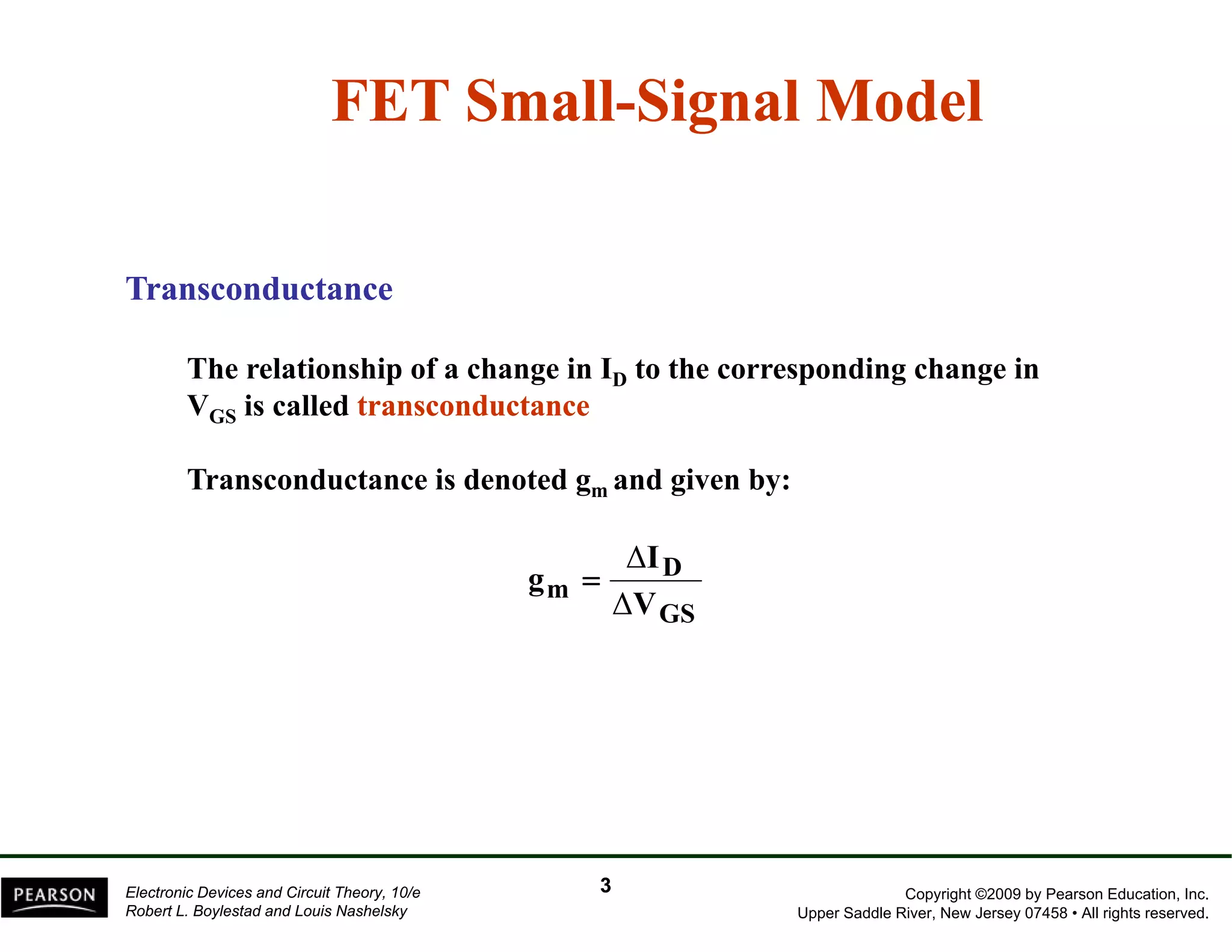
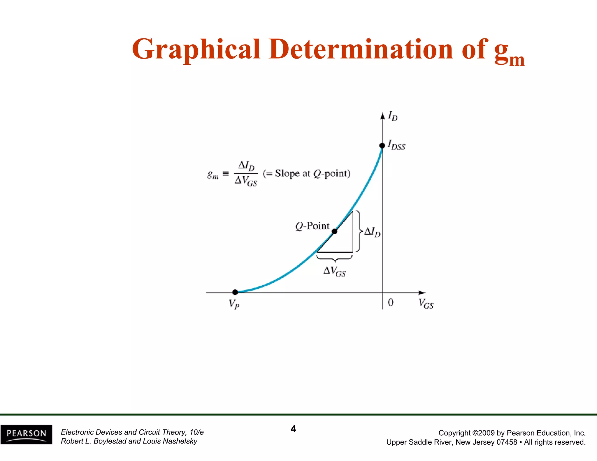
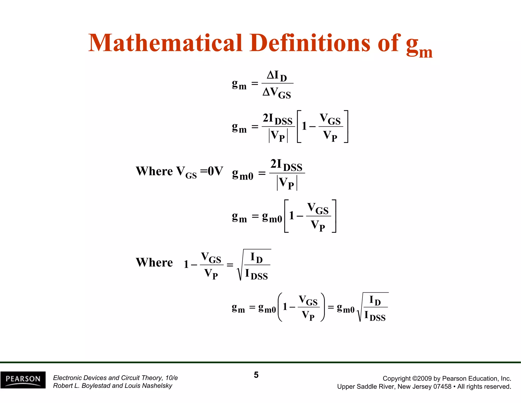
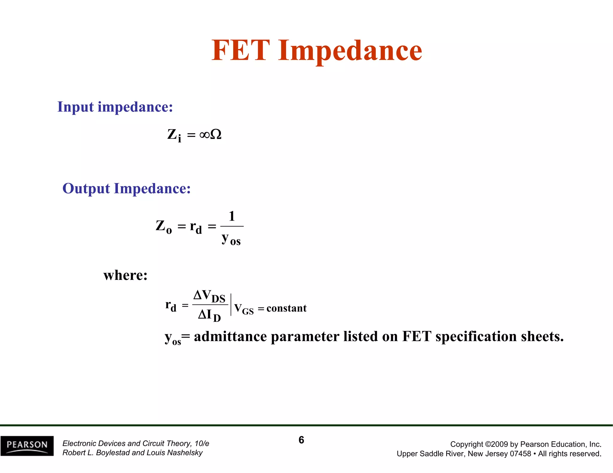
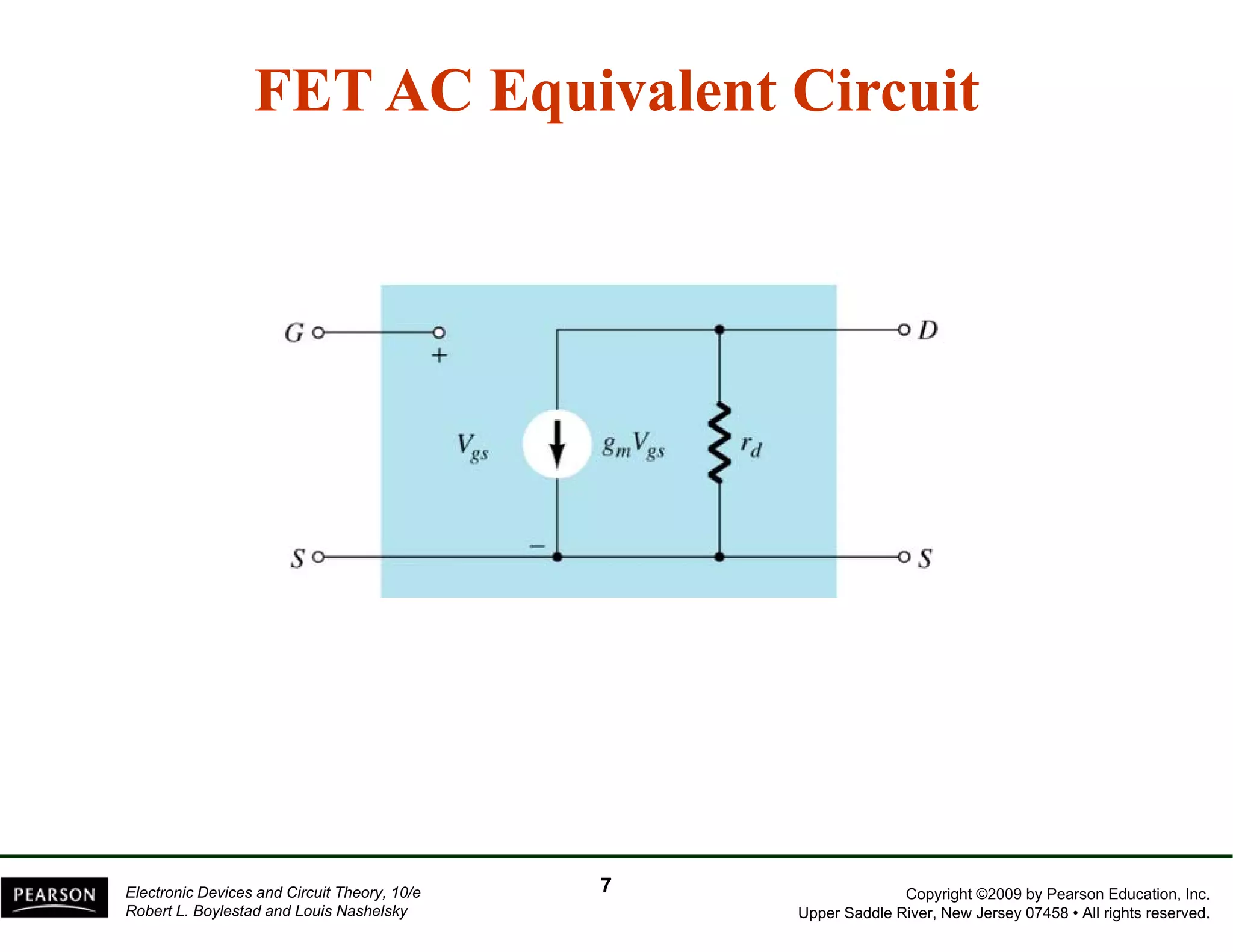
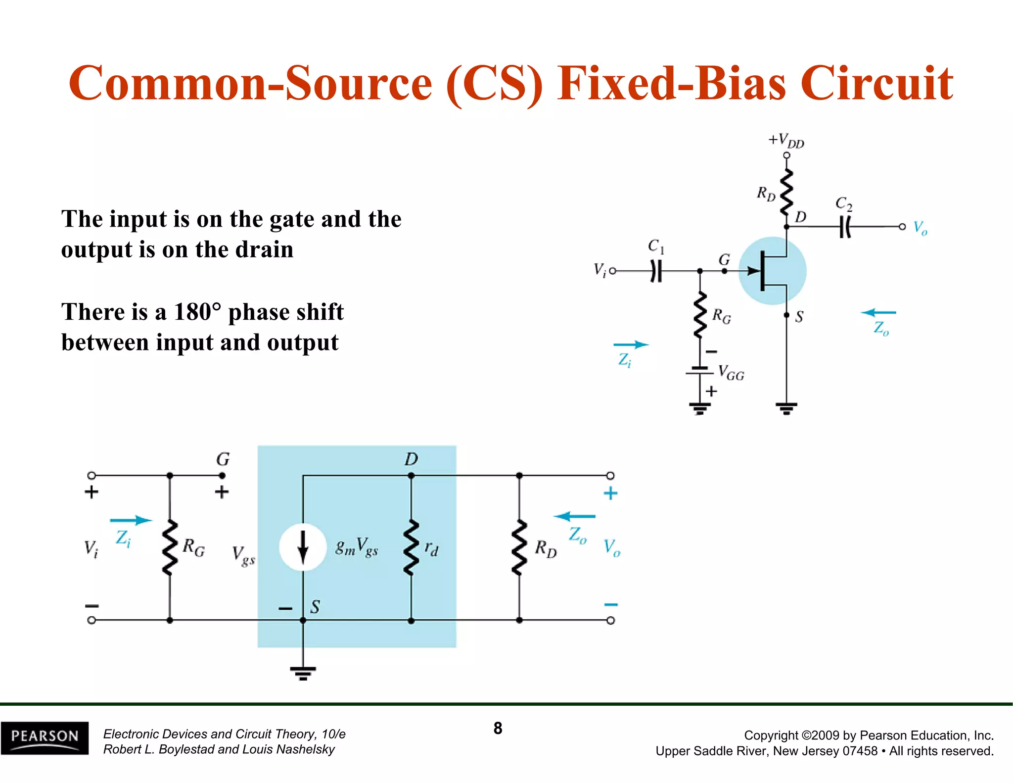
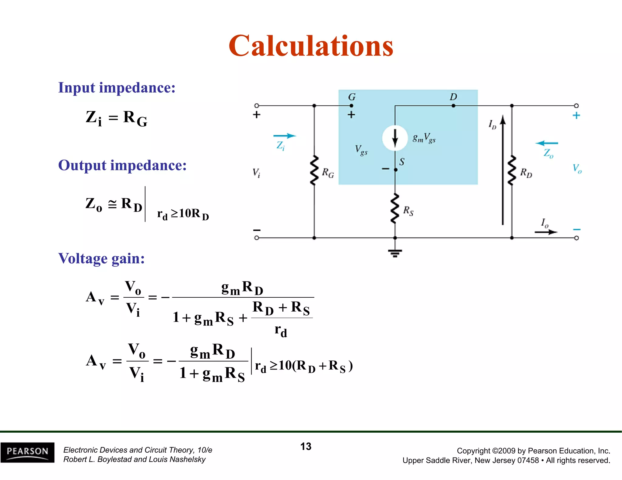
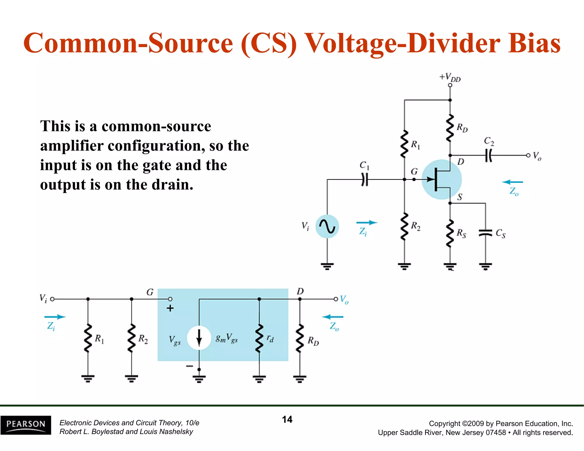
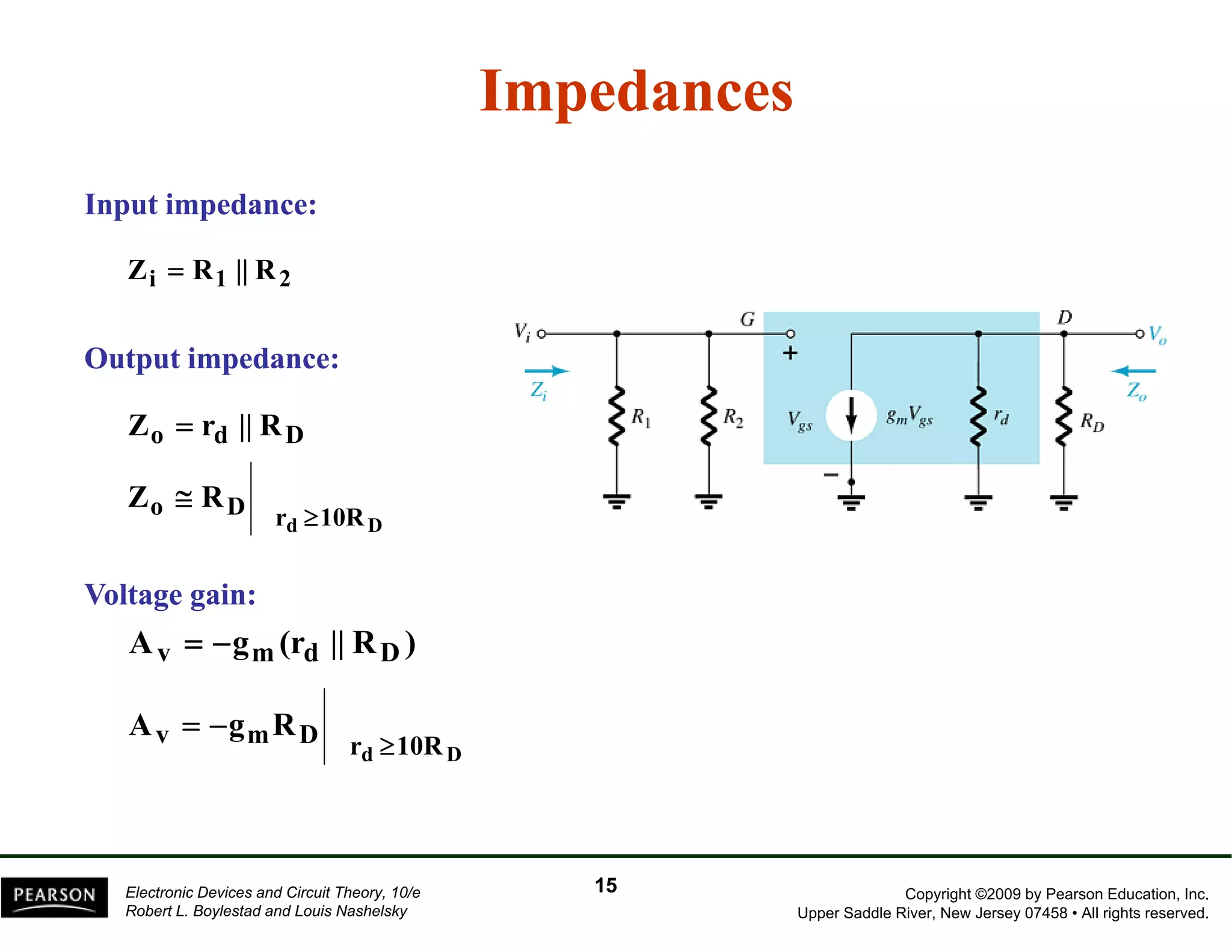
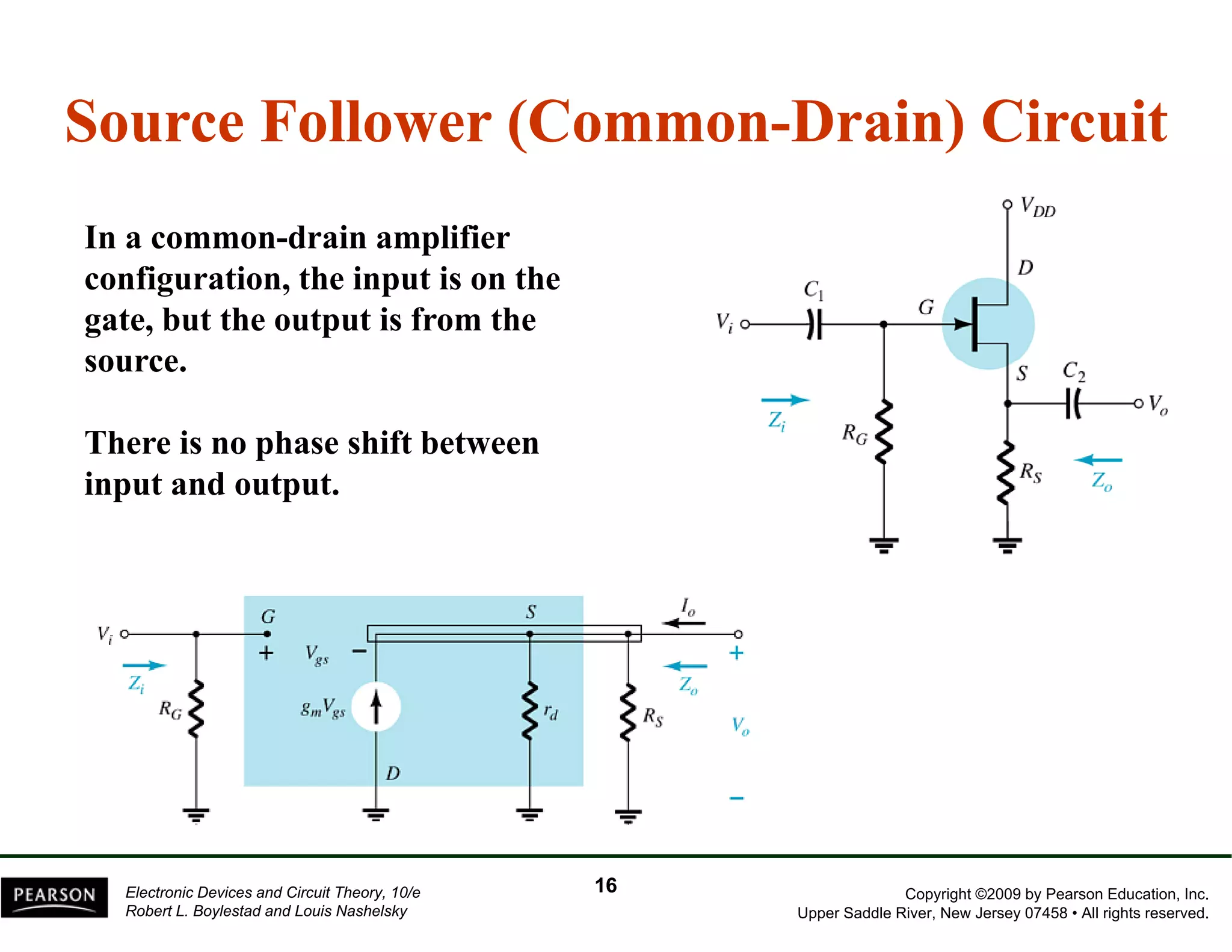
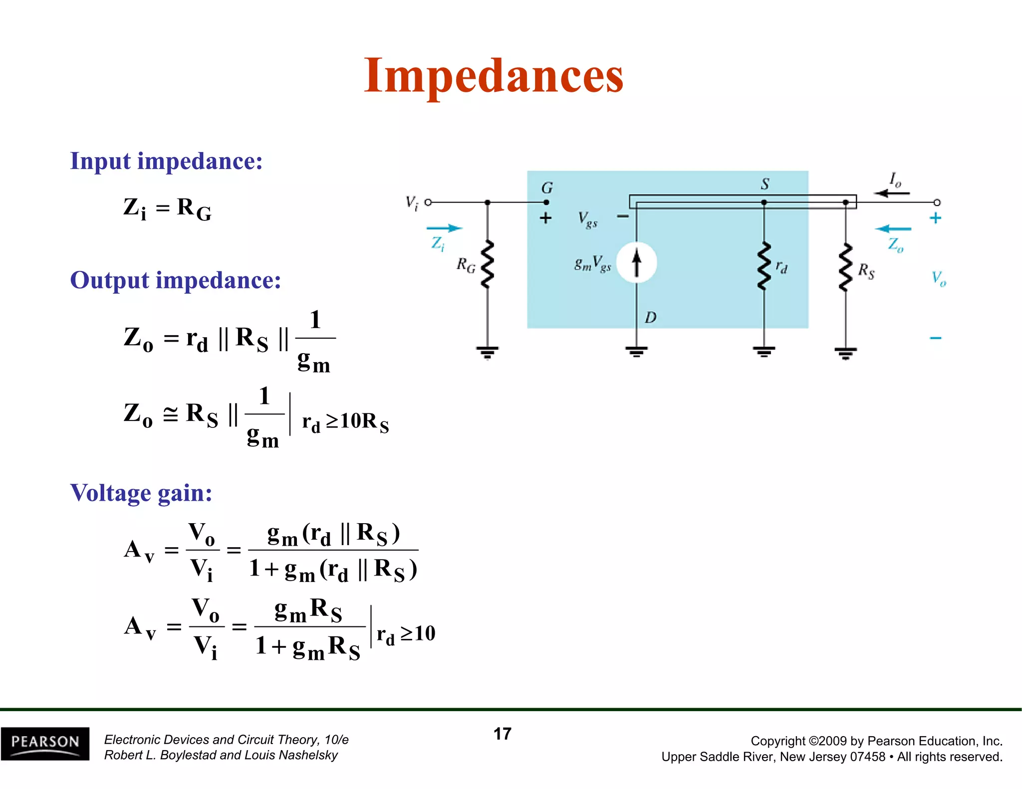
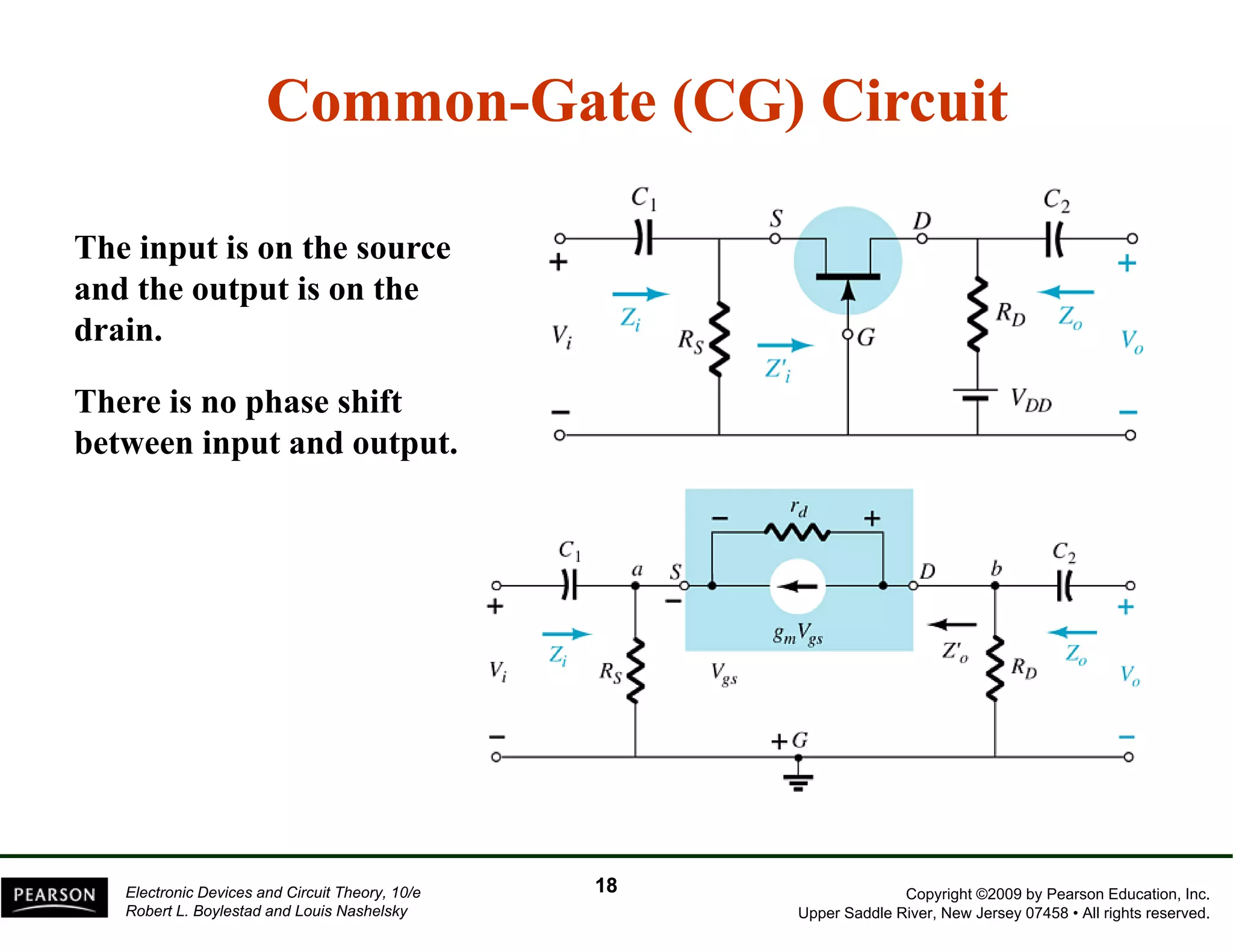
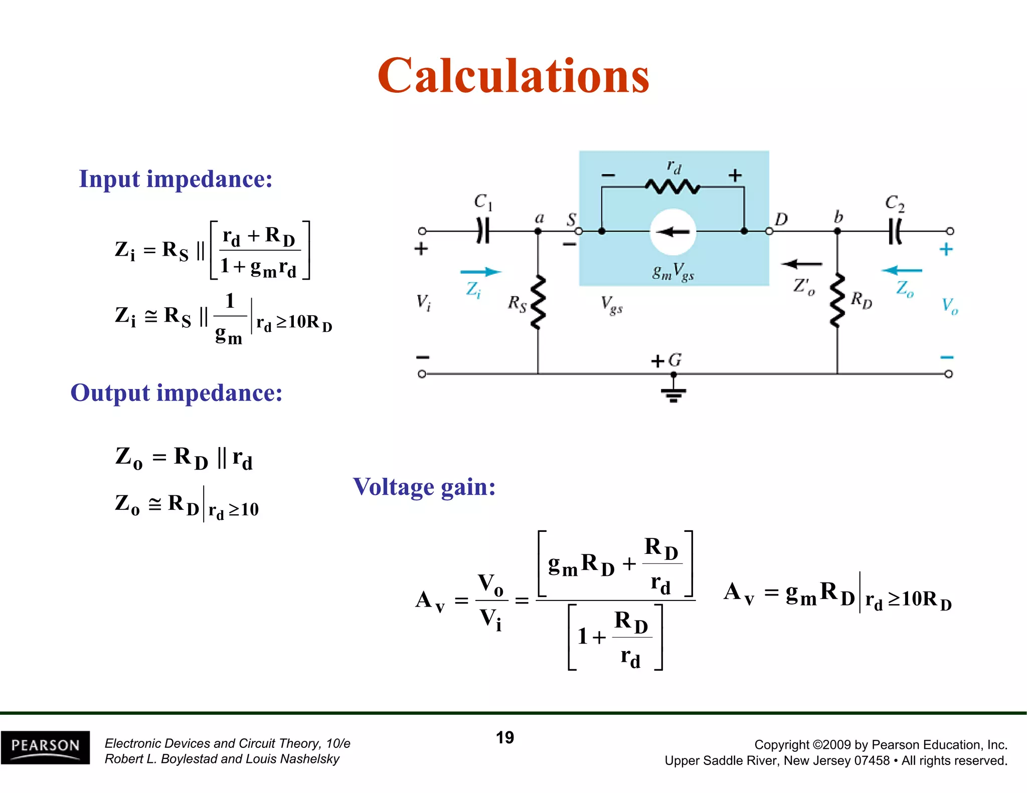
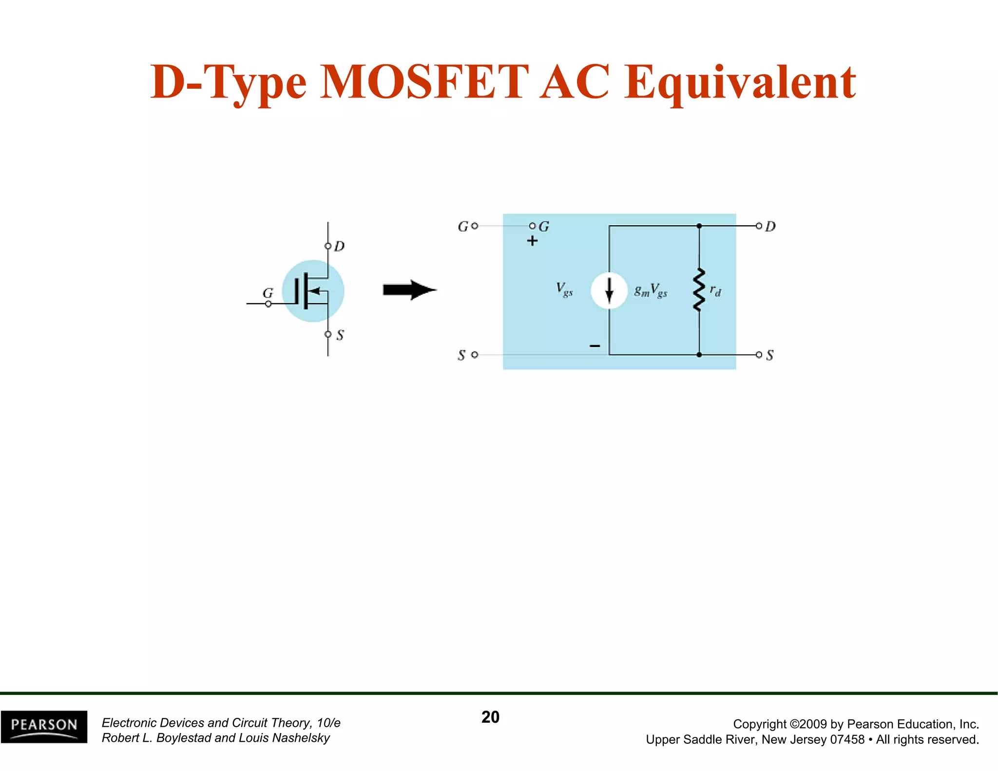
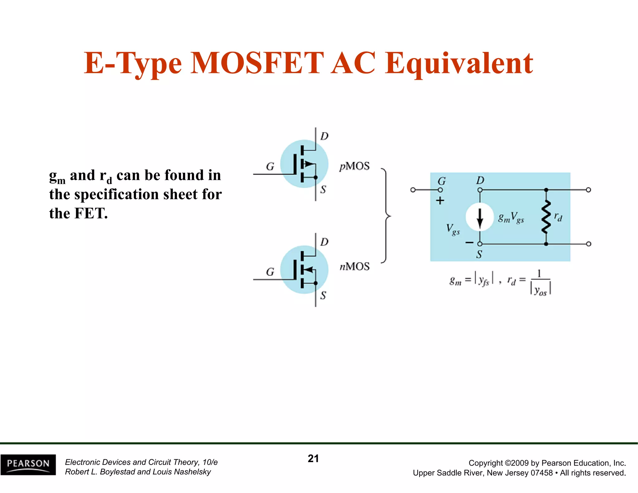
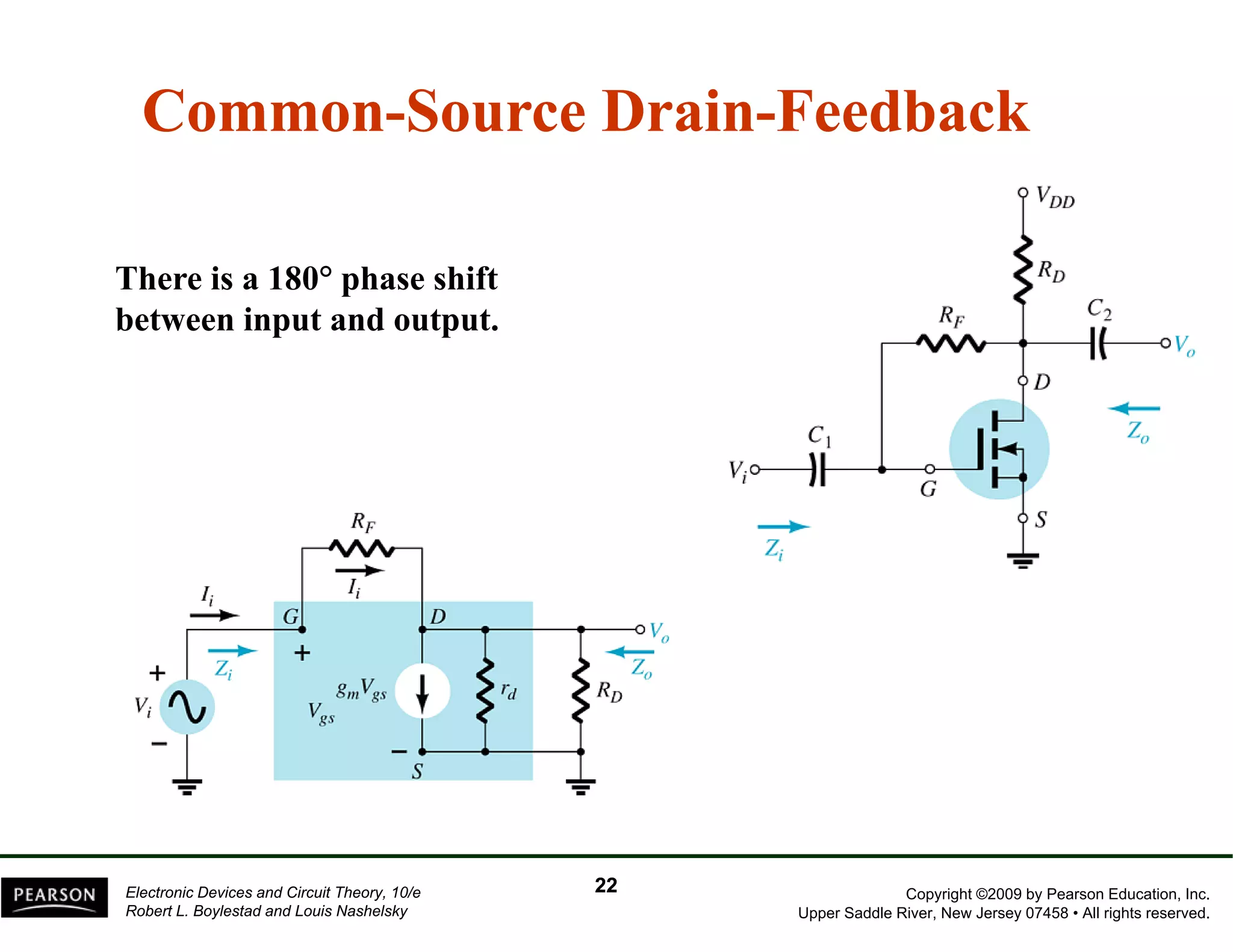
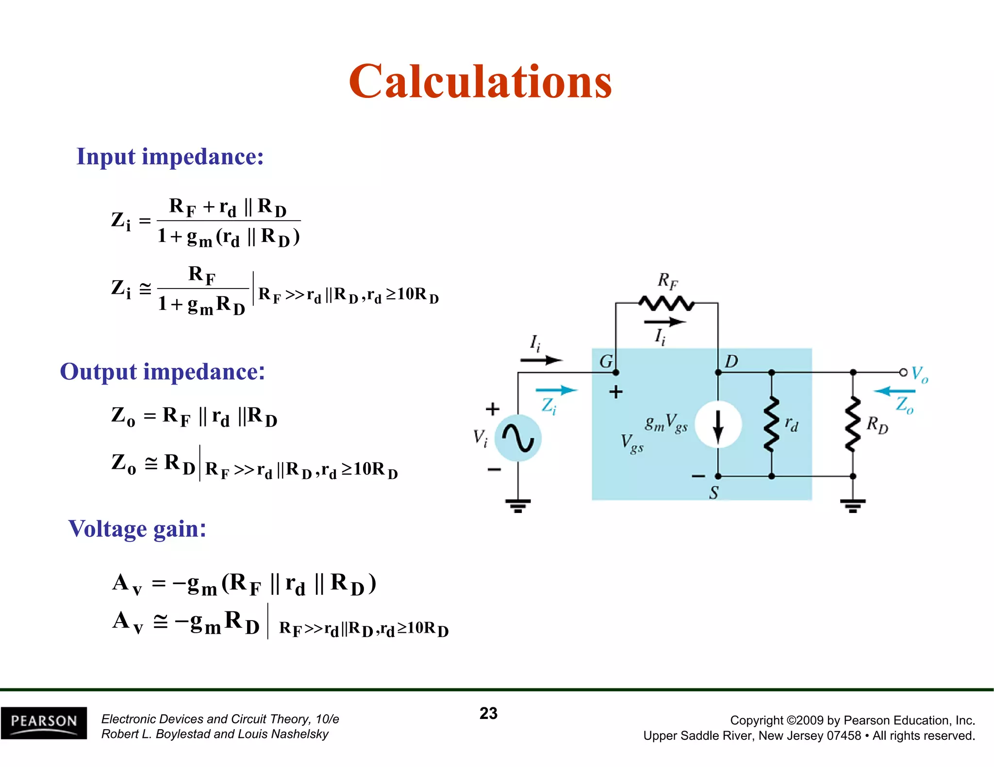
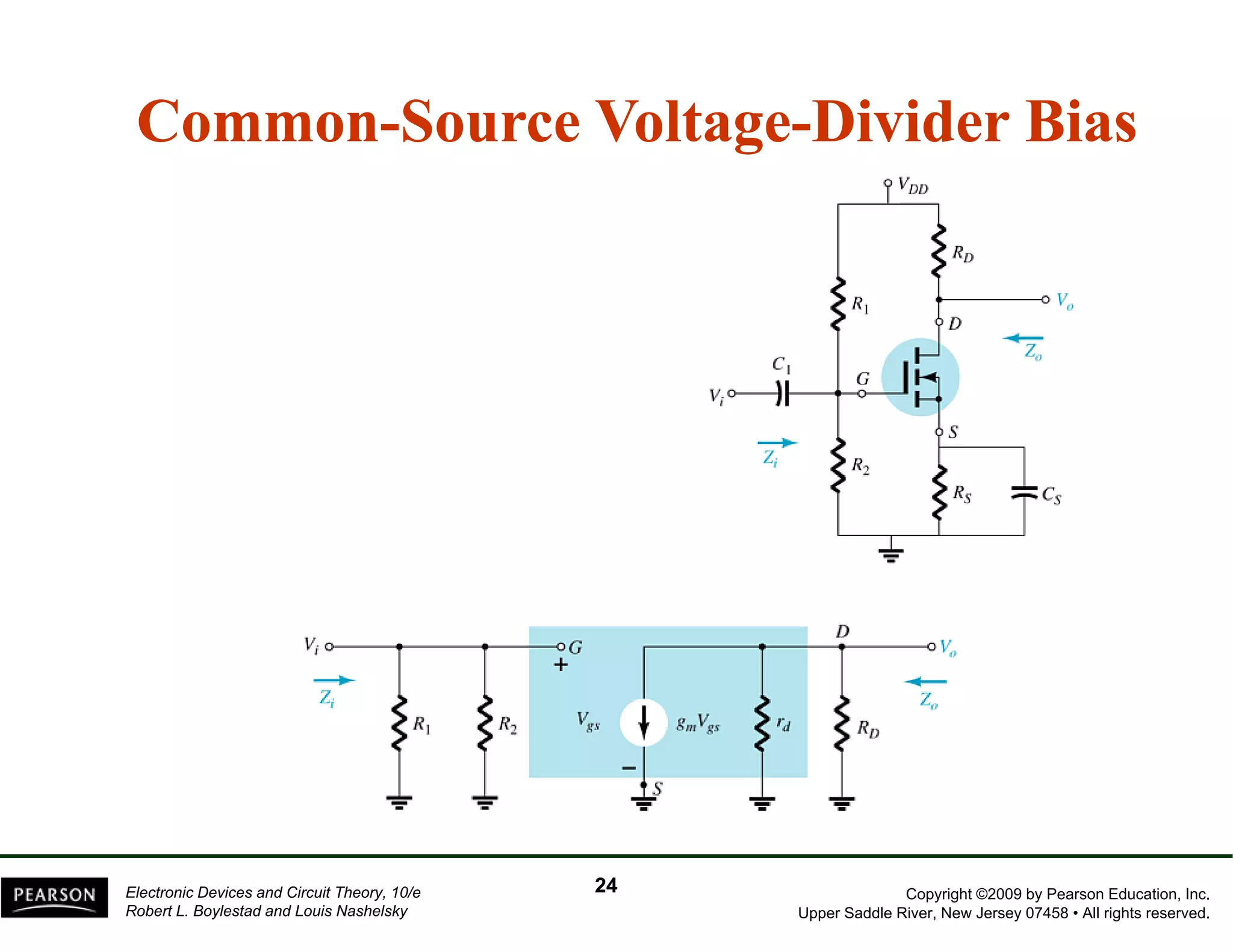
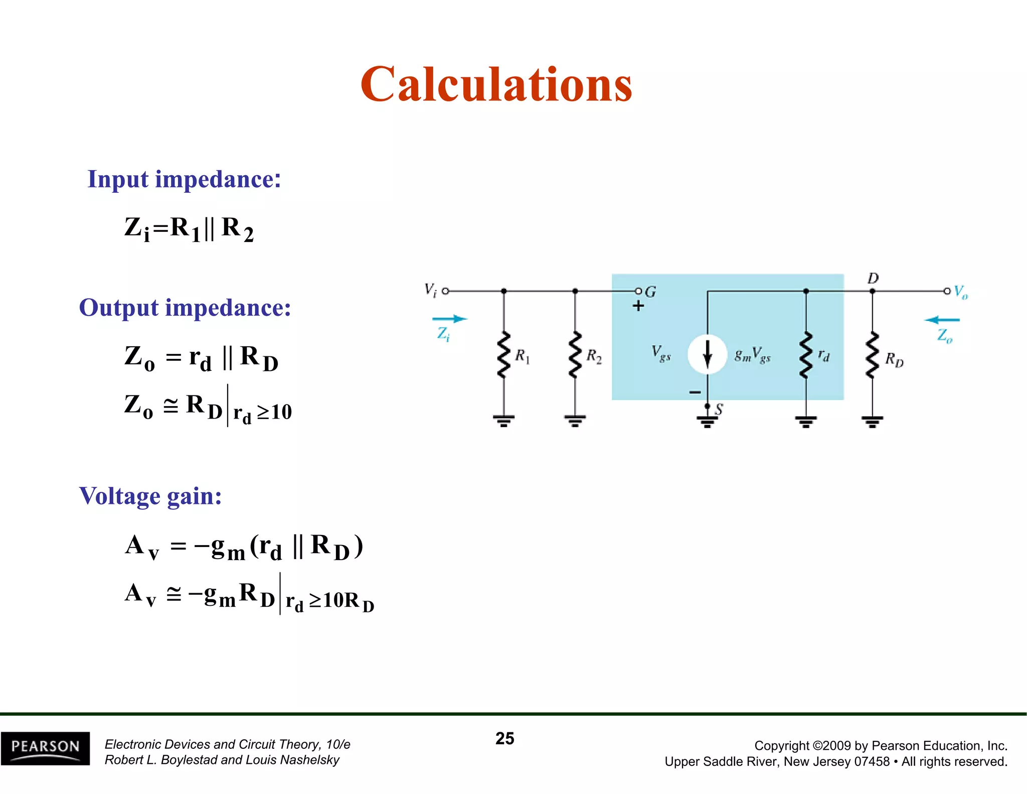
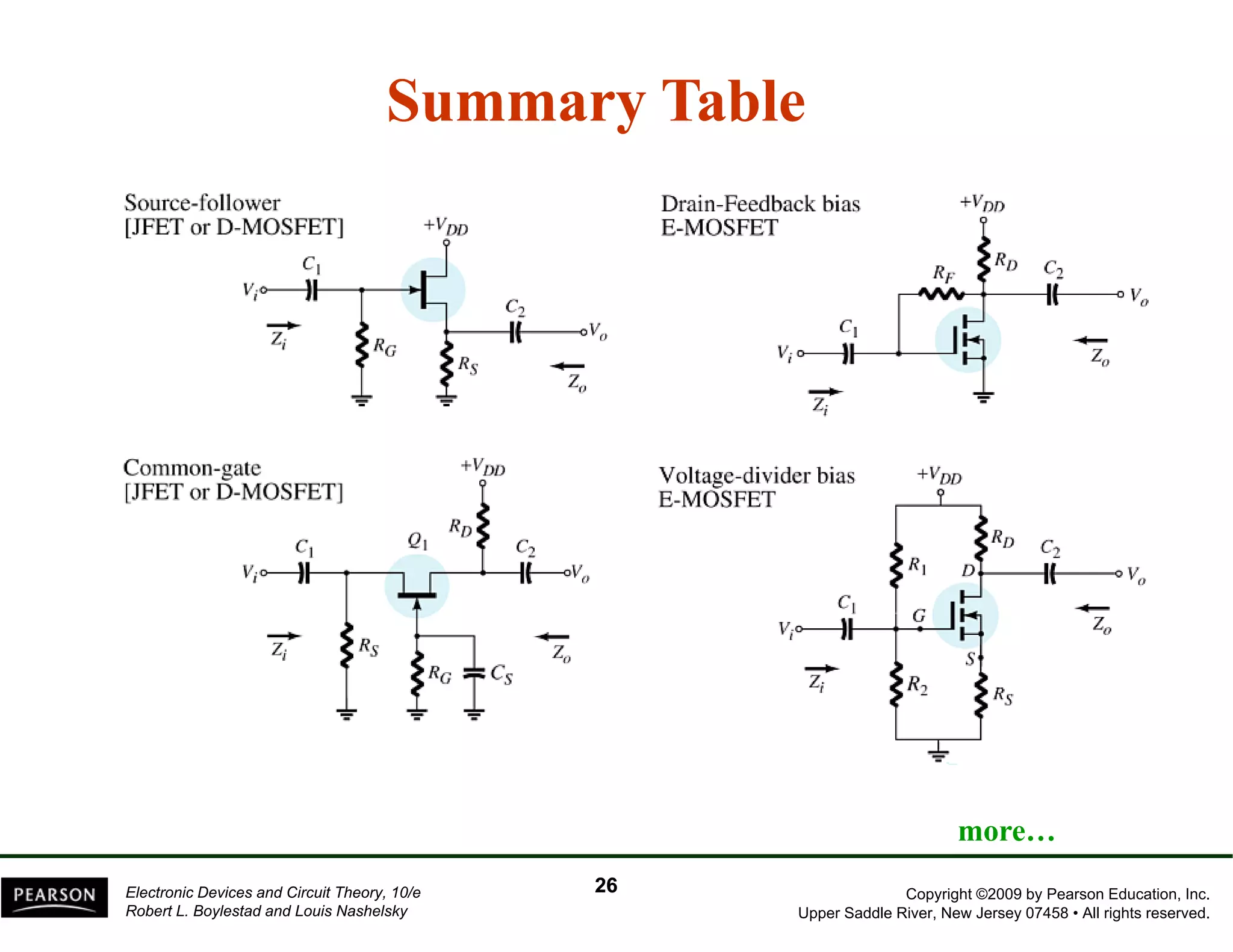
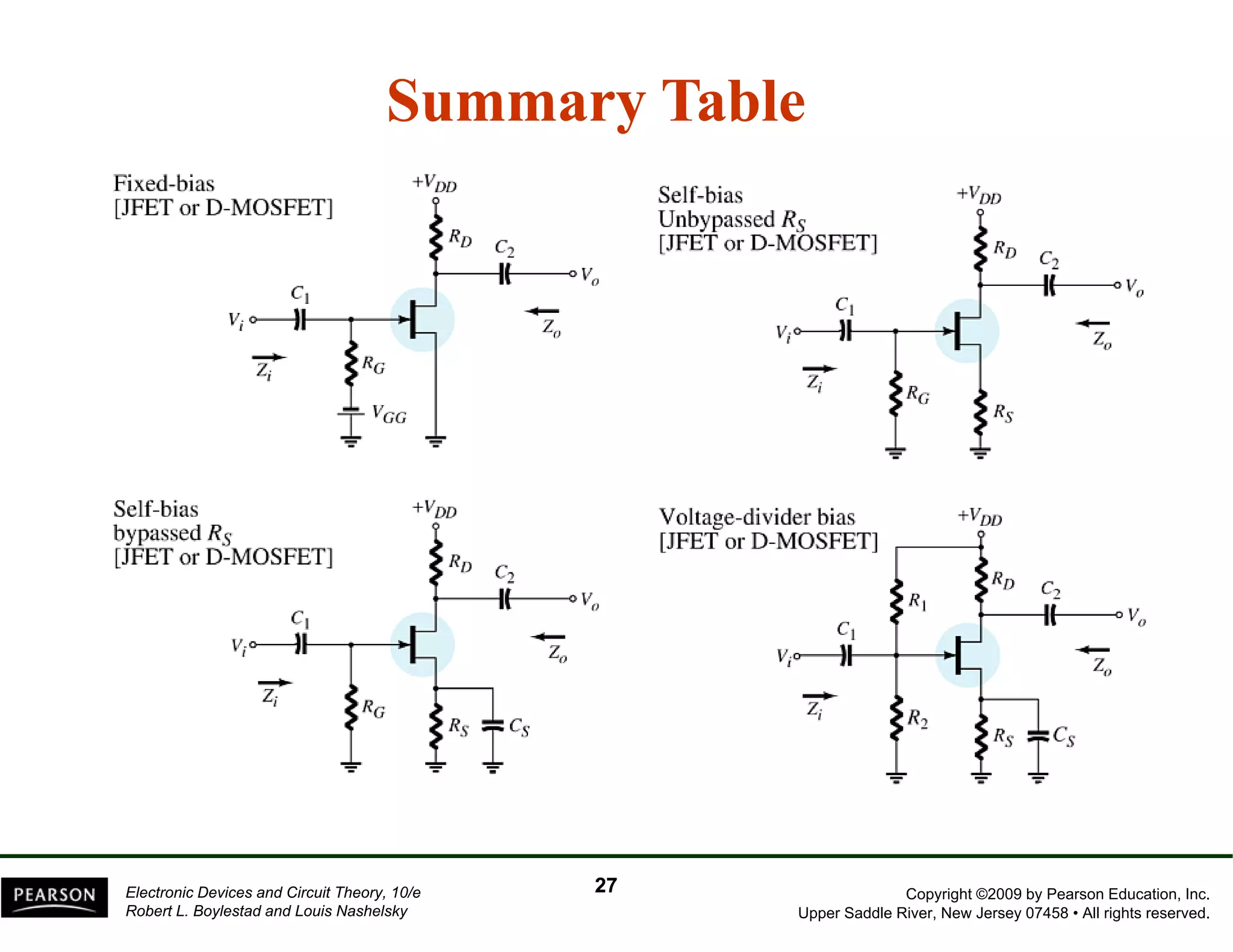

This chapter discusses FET amplifiers. It describes the common FET configurations including common-source, common-gate, and common-drain. It provides the small-signal models and defines terms like transconductance. It then gives the input and output impedances and voltage gain calculations for each configuration. Examples of biased circuits are also presented along with a troubleshooting guide.


![RF Circuit Design - [Ch2-2] Smith Chart](https://cdn.slidesharecdn.com/ss_thumbnails/ch2-2-150613064401-lva1-app6891-thumbnail.jpg?width=640&height=640&fit=bounds)


