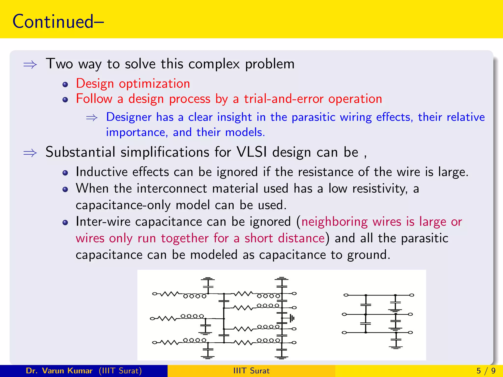
Determining and Quantifying Interconnect Parameters
Dr. Varun Kumar
Dr. Varun Kumar (IIIT Surat) IIIT Surat 1 / 9
Outlines
1 Introduction
2 Key Points for VLSI Design
3 Interconnect Parameters - Capacitance, Resistance, and Inductance
Dr. Varun Kumar (IIIT Surat) IIIT Surat 2 / 9
Introduction
⇒ Deep sub-micron semiconductor technologies causes rapid growth in
the field of VLSI.
⇒ Wires as a circuit components display a scaling behavior.
⇒ Active devices such as transistors,
Improvise gain
Reduces the device dimension
Improve the circuit speed
⇒ Larger die sizes economically feasible
Increase in the average length of an interconnect wire (parasitic effects)
Dr. Varun Kumar (IIIT Surat) IIIT Surat 3 / 9
Key points
⇒ Heavily doped n+ or p+ layers, typically used for the realization of
source and drain regions.
It can be employed for wiring purposes.
These wires have no apparent impact on the circuit performance.
⇒ Integrated circuits has a complex geometry that introduces
Capacitive ⇒ Impact on the energy dissipation and the power
distribution.
Resistive ⇒ Increase in propagation delay
Inductive ⇒ An introduction of extra noise sources, which affects the
reliability of the circuit.
⇒ For todays integrated circuits with their millions of circuit nodes, it
becomes useless.
⇒ The circuit behavior at a given circuit node is only determined by a
few dominant parameters.
Dr. Varun Kumar (IIIT Surat) IIIT Surat 4 / 9
Continued–
⇒ Two way to solve this complex problem
Design optimization
Follow a design process by a trial-and-error operation
⇒ Designer has a clear insight in the parasitic wiring effects, their relative
importance, and their models.
⇒ Substantial simplifications for VLSI design can be ,
Inductive effects can be ignored if the resistance of the wire is large.
When the interconnect material used has a low resistivity, a
capacitance-only model can be used.
Inter-wire capacitance can be ignored (neighboring wires is large or
wires only run together for a short distance) and all the parasitic
capacitance can be modeled as capacitance to ground.
Dr. Varun Kumar (IIIT Surat) IIIT Surat 5 / 9
Interconnect Parameters - Capacitance, Resistance, and Inductance
Capacitance
⇒ An accurate modeling of the wire capacitance(s) is a non-trivial task.
⇒ The capacitance of such a wire is a function of
Shape
Environment
Distance to the substrate
Distance to surrounding wires
⇒ If W >> tdi the electrical-field lines are orthogonal to the capacitor
plates, and that its capacitance can be modeled by the parallel-plate
capacitor
Dr. Varun Kumar (IIIT Surat) IIIT Surat 6 / 9
Continued–
Resistance
⇒ The resistance of a wire is proportional to its length L and inversily
proportional to its cross-section A.
R = ρ
L
A
 ρ → Resistivity of the material
⇒ Aluminum is the most common interconnect material.
Low cost
Compatibility with the standard IC fabrication process
Material ρ (Ω-m)
Silver (Ag) 1.6 ×10⁻⁸
Copper (Cu) 1.7 ×10⁻⁸
Gold (Au) 2.2×10⁻⁸
Aluminum (Al) 2.7×10⁻⁸
Tungsten (W) 5.5×10⁻⁸
Dr. Varun Kumar (IIIT Surat) IIIT Surat 7 / 9
Skin effect for different width of conductor
δ =
r
ρ
πf µ
Dr. Varun Kumar (IIIT Surat) IIIT Surat 8 / 9
Continued–
Inductance
Inductance starts to play a role on a chip.
Adoption of low-resistive interconnect materials
Increasing of switching frequencies (GHz order)
Dr. Varun Kumar (IIIT Surat) IIIT Surat 9 / 9

Interconnect Parameter in Digital VLSI Design

  • 1.
    Determining and QuantifyingInterconnect Parameters Dr. Varun Kumar Dr. Varun Kumar (IIIT Surat) IIIT Surat 1 / 9
  • 2.
    Outlines 1 Introduction 2 KeyPoints for VLSI Design 3 Interconnect Parameters - Capacitance, Resistance, and Inductance Dr. Varun Kumar (IIIT Surat) IIIT Surat 2 / 9
  • 3.
    Introduction ⇒ Deep sub-micronsemiconductor technologies causes rapid growth in the field of VLSI. ⇒ Wires as a circuit components display a scaling behavior. ⇒ Active devices such as transistors, Improvise gain Reduces the device dimension Improve the circuit speed ⇒ Larger die sizes economically feasible Increase in the average length of an interconnect wire (parasitic effects) Dr. Varun Kumar (IIIT Surat) IIIT Surat 3 / 9
  • 4.
    Key points ⇒ Heavilydoped n+ or p+ layers, typically used for the realization of source and drain regions. It can be employed for wiring purposes. These wires have no apparent impact on the circuit performance. ⇒ Integrated circuits has a complex geometry that introduces Capacitive ⇒ Impact on the energy dissipation and the power distribution. Resistive ⇒ Increase in propagation delay Inductive ⇒ An introduction of extra noise sources, which affects the reliability of the circuit. ⇒ For todays integrated circuits with their millions of circuit nodes, it becomes useless. ⇒ The circuit behavior at a given circuit node is only determined by a few dominant parameters. Dr. Varun Kumar (IIIT Surat) IIIT Surat 4 / 9
  • 5.
    Continued– ⇒ Two wayto solve this complex problem Design optimization Follow a design process by a trial-and-error operation ⇒ Designer has a clear insight in the parasitic wiring effects, their relative importance, and their models. ⇒ Substantial simplifications for VLSI design can be , Inductive effects can be ignored if the resistance of the wire is large. When the interconnect material used has a low resistivity, a capacitance-only model can be used. Inter-wire capacitance can be ignored (neighboring wires is large or wires only run together for a short distance) and all the parasitic capacitance can be modeled as capacitance to ground. Dr. Varun Kumar (IIIT Surat) IIIT Surat 5 / 9
  • 6.
    Interconnect Parameters -Capacitance, Resistance, and Inductance Capacitance ⇒ An accurate modeling of the wire capacitance(s) is a non-trivial task. ⇒ The capacitance of such a wire is a function of Shape Environment Distance to the substrate Distance to surrounding wires ⇒ If W >> tdi the electrical-field lines are orthogonal to the capacitor plates, and that its capacitance can be modeled by the parallel-plate capacitor Dr. Varun Kumar (IIIT Surat) IIIT Surat 6 / 9
  • 7.
    Continued– Resistance ⇒ The resistanceof a wire is proportional to its length L and inversily proportional to its cross-section A. R = ρ L A ρ → Resistivity of the material ⇒ Aluminum is the most common interconnect material. Low cost Compatibility with the standard IC fabrication process Material ρ (Ω-m) Silver (Ag) 1.6 ×10⁻⁸ Copper (Cu) 1.7 ×10⁻⁸ Gold (Au) 2.2×10⁻⁸ Aluminum (Al) 2.7×10⁻⁸ Tungsten (W) 5.5×10⁻⁸ Dr. Varun Kumar (IIIT Surat) IIIT Surat 7 / 9
  • 8.
    Skin effect fordifferent width of conductor δ = r ρ πf µ Dr. Varun Kumar (IIIT Surat) IIIT Surat 8 / 9
  • 9.
    Continued– Inductance Inductance starts toplay a role on a chip. Adoption of low-resistive interconnect materials Increasing of switching frequencies (GHz order) Dr. Varun Kumar (IIIT Surat) IIIT Surat 9 / 9