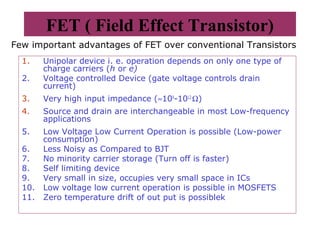
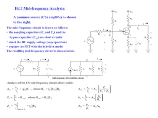
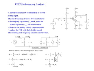
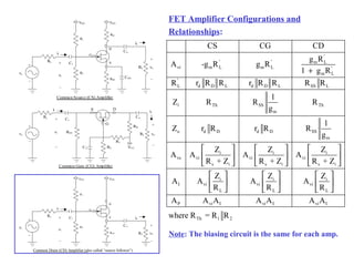
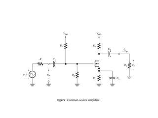
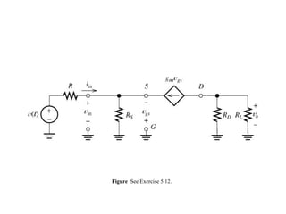
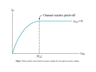
The document describes the Field Effect Transistor (FET). Key points:
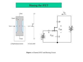
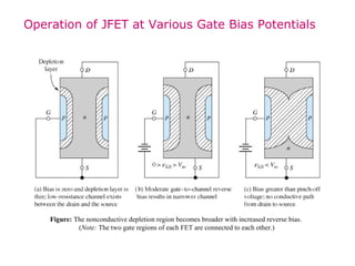
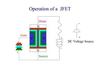
1. FET is a voltage-controlled, unipolar semiconductor device with very high input impedance. Current flow depends on an electric field rather than injection of minority carriers.
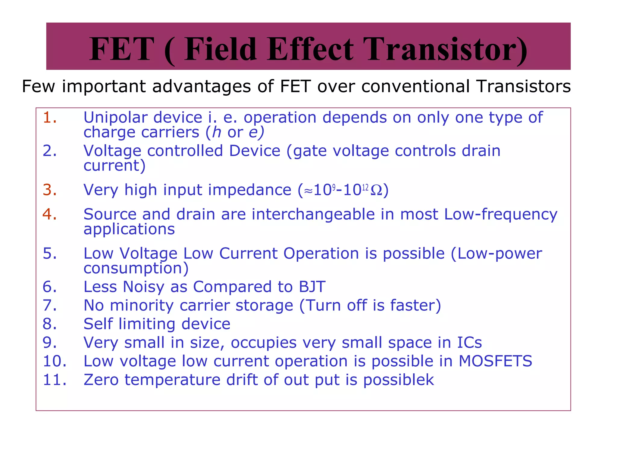
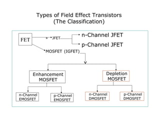
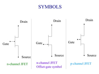
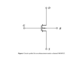
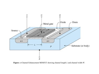
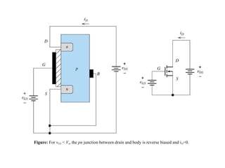
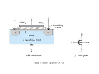
2. There are two main types - JFET and MOSFET. JFET uses a P-N junction for controlling the electric field while MOSFET uses a metal-oxide-semiconductor structure.
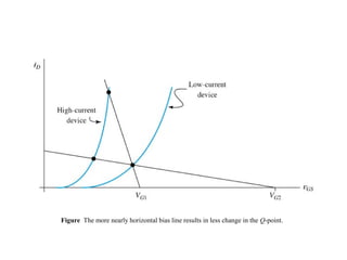
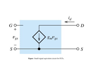
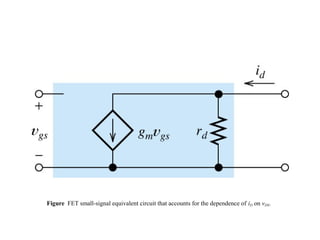
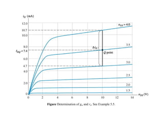
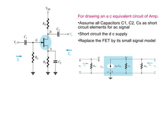
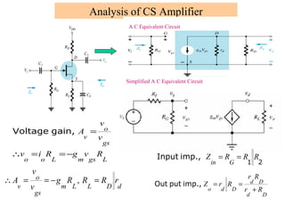
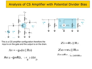
3. FETs have advantages over BJTs like lower power consumption, faster switching, smaller size. Analysis of FET circuits involves determining the small-signal parameters like transconductance gm and output resistance rd.