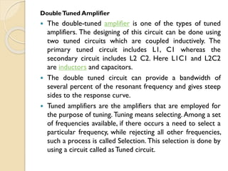
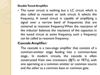
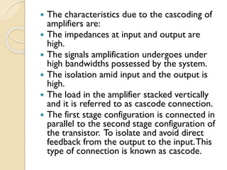
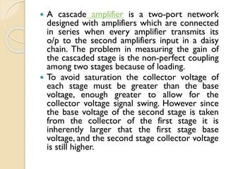
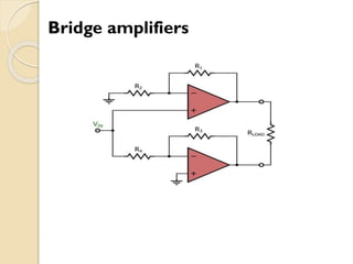
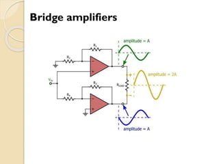
The document discusses various topics related to analog electronics including:
1. Transistor biasing methods such as base resistor, collector to base, fixed bias, and voltage divider bias.
2. Amplifier configurations including common base, common emitter, and common collector. Characteristics of the common emitter configuration are also discussed.
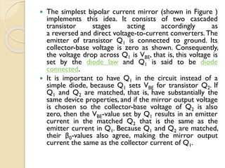
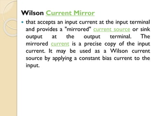
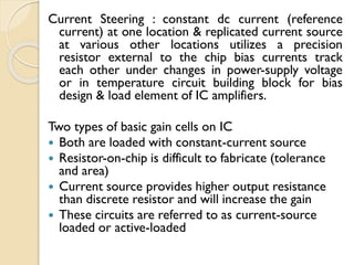
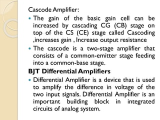
3. IC biasing using current sources and current mirrors. Basic gain cell and cascode amplifiers are introduced.

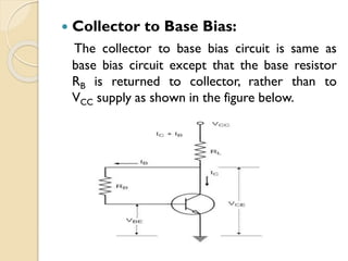


![[Deck] What's New in Spark-Iceberg Integration via DSV2.pptx](https://cdn.slidesharecdn.com/ss_thumbnails/deckwhatsnewinspark-icebergintegrationviadsv2-260210005337-25955b12-thumbnail.jpg?width=640&height=640&fit=bounds)


