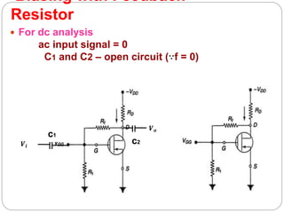
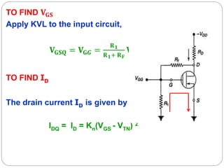
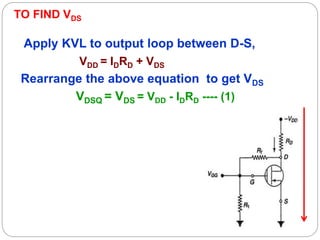
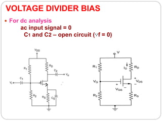
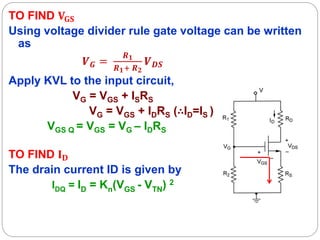
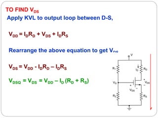
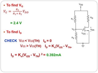
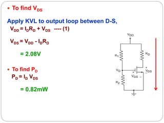
R.M.K. COLLEGE OF
ENGINEERING AND TECHNOLOGY
MOSFET BIAISING TECHNIQUES
Dr.N.G.Praveena
Associate Professor/ECE
MOSFET BIASING
 Voltage controlled device
 Different biasing circuit of MOSFET are
Biasing with Feedback Resistor
Voltage Divider Bias
ID For enhancement-type
MOSFETs
Non saturation
region
(VDS < VDS (sat) )
ID = Kn [ 2 (VGS - VTN) VDS – V2
DS ]
Saturation region
(VDS > VDS (sat) )
ID = Kn(VGS - VTN) 2
Transition point VDS(sat) = VGS – VTN
Enhancement mode VTN > 0
Depletion mode VTN < 0
Biasing with Feedback
Resistor
 For dc analysis
ac input signal = 0
C1 and C2 – open circuit (∵f = 0)
𝑽𝒐
𝑽𝒊
c2
c1
TO FIND 𝐕𝐆𝐒
Apply KVL to the input circuit,
𝐕𝐆𝐒𝐐 = 𝐕𝐆𝑮 =
𝐑𝟏
𝐑𝟏+ 𝐑𝐅
𝐕𝐃𝐒
TO FIND ID
The drain current ID is given by
IDQ = ID = Kn(VGS - VTN) 2
TO FIND VDS
Apply KVL to output loop between D-S,
VDD = IDRD + VDS
Rearrange the above equation to get VDS
VDSQ = VDS = VDD - IDRD ---- (1)
DC LOAD LINE AND Q POINT
To find point A
Sub VDS = 0 in (1)
VDD = IDRD
ID = VDD/ RD
Pt. A = (0, VDD/ RD )
To find point B
Sub ID = 0 in (1)
VDS = VDD
Pt. B = (VDD , 0)
VDS = VDD - IDRD ----
(1)
(0, VDD/ RD)
(VDD ,0) VDS
ID
A
B
VOLTAGE DIVIDER BIAS
 For dc analysis
ac input signal = 0
C1 and C2 – open circuit (∵f = 0)
TO FIND 𝐕𝐆𝐒
Using voltage divider rule gate voltage can be written
as
𝑽𝑮 =
𝑹𝟏
𝑹𝟏+ 𝑹𝟐
𝑽𝑫𝑺
Apply KVL to the input circuit,
VG = VGS + ISRS
VG = VGS + IDRS (∴ID=IS )
VGS Q = VGS = VG – IDRS
TO FIND 𝐈𝐃
The drain current ID is given by
IDQ = ID = Kn(VGS - VTN) 2
TO FIND VDS
Apply KVL to output loop between D-S,
VDD = IDRD + VDS + IDRS
Rearrange the above equation to get VDS
VDS = VDD - IDRD – IDRS
VDSQ = VDS = VDD – ID (RD + RS)
Problems
Calculate the drain current and drain-to-source voltage
of a common-source circuit with an n-channel
enhancement mode MOSFET. Find the power
dissipated in the transistor. Assume that 𝑹𝟏 = 30 kΩ,
𝑹𝟐 = 20 k Ω , 𝑹𝑫 = 10 k Ω , 𝑽𝑫𝑫 = 6 V, 𝑽𝑮𝑺(𝑻𝑯) = 1 V and k
= 0.2 mA/ V2
Given data:
 𝑽𝑫𝑫 = 6V ;
 𝑹𝑫 = 10KΩ ;
 𝑹𝟏 = 30KΩ
 𝑹𝟐 = 20kΩ ;
 𝑽𝑮𝑺(𝑻𝑯)= 1V
 K = 0.2 mA/ V2
 To find VG
𝑉𝐺 =
𝑅2
𝑅1+ 𝑅2
𝑉𝐷𝐷
= 2.4 V
 To find ID
CHECK VGS < VGS(TH) ID = 0
VGS > VGS(TH) ID = Kn(VGS - VTN) 2
ID = Kn(VGS - VTN) 2 = 0.392mA
 To find VDS
Apply KVL to output loop between D-S,
VDD = IDRD + VDS ---- (1)
VDS = VDD - IDRD
= 2.08V
 To find PD
PD = ID VDS
= 0.82mW
DC LOAD LINE
VDD = IDRD + VDS ----(1)
To find point A
Sub VDS = 0 in (1)
VDD = IDRD
ID = VDD/ RD
= 0.6mA
Pt. A = (0, 0.6mA)
To find point B
Sub ID = 0 in (2)
VDS = VDD
= 6V
Pt. B = ( 6V , 0)
(0, VDD/ RD)
(VDD ,0) VDS
ID
0.6mA
6V
IDQ =0.392mA
VDSQ =2.08V
VGSQ =2.4V
A
B
BJT SWITCHING CIRCUIT
 The application of transistor is not limited solely to
the amplification of signals.
 Through proper design transistors can be used as
switches for computer and control application.
 The network shown in fig. can be employed as an
inverter in computer logic circuitry , note that
output voltage VO is opposite to that applied to the
base or input terminal.
 Proper design for the inversion process requires
that the operating point switch from cutoff to
Transistor Inverter Circuit
Saturation condition and the
resulting terminal resistance
Cutoff condition and the
resulting terminal resistance
THERMAL STABILITY
• The power dissipated within a transistor is
predominantly the power dissipated at its collector
to base junction.
• Thus maximum power is limited by the
temperature that the collector –base junction can
withstand.(For Silicon - 150 to 2550C and
Germanium - 60 to 1000C)
• The collector-base junction temperature may rise
because of two reasons.
 Due to rise in ambient temperature
Thermal Resistance
 At steady state the temperature rise at the collector
junction is proportional to the power dissipated at
the junction.
Tj – TA = 𝜽 PD
Where Tj - Junction temperature in 0C
TA - Ambient temperature in 0C
PD - Dissipated power in watt
θ - Constant of proportionality
 θ is constant of proportionality which is referred as
thermal resistance
𝜽 =
Tj – TA
PD
Condition for thermal stability
 The required condition to avoid thermal runaway
is that the rate at which heat is released at the
collector junction must not exceed the rate at
which the heat can be dissipated.
𝛛𝐏𝐂
𝛛𝐓𝐉
<
𝛛𝐏𝐃
𝛛𝐓𝐉

Mosfet baising

  • 1.
    R.M.K. COLLEGE OF ENGINEERINGAND TECHNOLOGY MOSFET BIAISING TECHNIQUES Dr.N.G.Praveena Associate Professor/ECE
  • 2.
    MOSFET BIASING  Voltagecontrolled device  Different biasing circuit of MOSFET are Biasing with Feedback Resistor Voltage Divider Bias
  • 3.
    ID For enhancement-type MOSFETs Nonsaturation region (VDS < VDS (sat) ) ID = Kn [ 2 (VGS - VTN) VDS – V2 DS ] Saturation region (VDS > VDS (sat) ) ID = Kn(VGS - VTN) 2 Transition point VDS(sat) = VGS – VTN Enhancement mode VTN > 0 Depletion mode VTN < 0
  • 4.
    Biasing with Feedback Resistor For dc analysis ac input signal = 0 C1 and C2 – open circuit (∵f = 0) 𝑽𝒐 𝑽𝒊 c2 c1
  • 5.
    TO FIND 𝐕𝐆𝐒 ApplyKVL to the input circuit, 𝐕𝐆𝐒𝐐 = 𝐕𝐆𝑮 = 𝐑𝟏 𝐑𝟏+ 𝐑𝐅 𝐕𝐃𝐒 TO FIND ID The drain current ID is given by IDQ = ID = Kn(VGS - VTN) 2
  • 6.
    TO FIND VDS ApplyKVL to output loop between D-S, VDD = IDRD + VDS Rearrange the above equation to get VDS VDSQ = VDS = VDD - IDRD ---- (1)
  • 7.
    DC LOAD LINEAND Q POINT To find point A Sub VDS = 0 in (1) VDD = IDRD ID = VDD/ RD Pt. A = (0, VDD/ RD ) To find point B Sub ID = 0 in (1) VDS = VDD Pt. B = (VDD , 0) VDS = VDD - IDRD ---- (1) (0, VDD/ RD) (VDD ,0) VDS ID A B
  • 8.
    VOLTAGE DIVIDER BIAS For dc analysis ac input signal = 0 C1 and C2 – open circuit (∵f = 0)
  • 9.
    TO FIND 𝐕𝐆𝐒 Usingvoltage divider rule gate voltage can be written as 𝑽𝑮 = 𝑹𝟏 𝑹𝟏+ 𝑹𝟐 𝑽𝑫𝑺 Apply KVL to the input circuit, VG = VGS + ISRS VG = VGS + IDRS (∴ID=IS ) VGS Q = VGS = VG – IDRS TO FIND 𝐈𝐃 The drain current ID is given by IDQ = ID = Kn(VGS - VTN) 2
  • 10.
    TO FIND VDS ApplyKVL to output loop between D-S, VDD = IDRD + VDS + IDRS Rearrange the above equation to get VDS VDS = VDD - IDRD – IDRS VDSQ = VDS = VDD – ID (RD + RS)
  • 11.
    Problems Calculate the draincurrent and drain-to-source voltage of a common-source circuit with an n-channel enhancement mode MOSFET. Find the power dissipated in the transistor. Assume that 𝑹𝟏 = 30 kΩ, 𝑹𝟐 = 20 k Ω , 𝑹𝑫 = 10 k Ω , 𝑽𝑫𝑫 = 6 V, 𝑽𝑮𝑺(𝑻𝑯) = 1 V and k = 0.2 mA/ V2 Given data:  𝑽𝑫𝑫 = 6V ;  𝑹𝑫 = 10KΩ ;  𝑹𝟏 = 30KΩ  𝑹𝟐 = 20kΩ ;  𝑽𝑮𝑺(𝑻𝑯)= 1V  K = 0.2 mA/ V2
  • 12.
     To findVG 𝑉𝐺 = 𝑅2 𝑅1+ 𝑅2 𝑉𝐷𝐷 = 2.4 V  To find ID CHECK VGS < VGS(TH) ID = 0 VGS > VGS(TH) ID = Kn(VGS - VTN) 2 ID = Kn(VGS - VTN) 2 = 0.392mA
  • 13.
     To findVDS Apply KVL to output loop between D-S, VDD = IDRD + VDS ---- (1) VDS = VDD - IDRD = 2.08V  To find PD PD = ID VDS = 0.82mW
  • 14.
    DC LOAD LINE VDD= IDRD + VDS ----(1) To find point A Sub VDS = 0 in (1) VDD = IDRD ID = VDD/ RD = 0.6mA Pt. A = (0, 0.6mA) To find point B Sub ID = 0 in (2) VDS = VDD = 6V Pt. B = ( 6V , 0) (0, VDD/ RD) (VDD ,0) VDS ID 0.6mA 6V IDQ =0.392mA VDSQ =2.08V VGSQ =2.4V A B
  • 15.
    BJT SWITCHING CIRCUIT The application of transistor is not limited solely to the amplification of signals.  Through proper design transistors can be used as switches for computer and control application.  The network shown in fig. can be employed as an inverter in computer logic circuitry , note that output voltage VO is opposite to that applied to the base or input terminal.  Proper design for the inversion process requires that the operating point switch from cutoff to
  • 16.
    Transistor Inverter Circuit Saturationcondition and the resulting terminal resistance Cutoff condition and the resulting terminal resistance
  • 17.
    THERMAL STABILITY • Thepower dissipated within a transistor is predominantly the power dissipated at its collector to base junction. • Thus maximum power is limited by the temperature that the collector –base junction can withstand.(For Silicon - 150 to 2550C and Germanium - 60 to 1000C) • The collector-base junction temperature may rise because of two reasons.  Due to rise in ambient temperature
  • 18.
    Thermal Resistance  Atsteady state the temperature rise at the collector junction is proportional to the power dissipated at the junction. Tj – TA = 𝜽 PD Where Tj - Junction temperature in 0C TA - Ambient temperature in 0C PD - Dissipated power in watt θ - Constant of proportionality  θ is constant of proportionality which is referred as thermal resistance 𝜽 = Tj – TA PD
  • 19.
    Condition for thermalstability  The required condition to avoid thermal runaway is that the rate at which heat is released at the collector junction must not exceed the rate at which the heat can be dissipated. 𝛛𝐏𝐂 𝛛𝐓𝐉 < 𝛛𝐏𝐃 𝛛𝐓𝐉