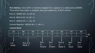
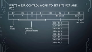
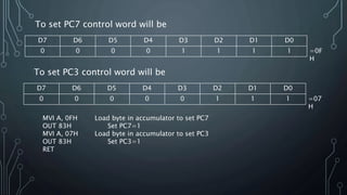
MICROPROCESSOR 8085
LECTURE 28
8255 PROGRAMMING EXAMPLES FOR DIFFERENT MODES
PROF. SANDIP DAS
WRITE A PROGRAM FOR IC 8255 TO READ DIP SWITCHES AND
DISPLAY THE READING FROM PORT B TO PORT A AND FROM
PORT 𝐶𝐿 AT PORT 𝐶 𝑈
8255
BufferBuffer
5V
5V
CSA1
5
A1
A0
𝑀𝐸𝑀𝑅
𝑀𝐸𝑀𝑊
RESET
PA
7
PA
0
PC
7
PC
4
PC
3
PC
0
PB7
PB0
Port Address: Since 8255 is memory mapped I/O, suppose it is addressed at 8000H.
Then when Chip select is enabled, then port addresses of 8255 will be-
Port A- 8000H (A1=0, A0=0)
Port B- 8001H (A1=0, A2=1)
Port C- 8002H (A1=1, A2=0)
Control Register- 8003H (A1=1, A0=1)
Control Word:
D7 D6 D5 D4 D3 D2 D1 D0
1 0 0 0 0 0 1 1
Port A in
Mode 0
Port
A=
Output
Port
𝐶 𝑈 =
Output
Port B
in
Mode 0
Port
B=
Input
Port
𝐶𝐿 =
Input
I/O
mode
=83
H
PROGRAM:
MVI A,83H Load accumulator with the control word
STA 8003H Write word in the control register to
initialize the ports
LDA 8001H Read switches at Port B
STA 8000H Display the reading at Port A
LDA 8002H Read switches at Port C
ANI 0FH Mask the upper four bits of Port C; these bits are not input
data
RLC
RLC
RLC
RLC
STA 8002H Display data at Port 𝐶 𝑈
HLT
WRITE A BSR CONTROL WORD TO SET BITS PC7 AND
PC0
D7 D6 D5 D4 D3 D2 D1 D0
0 X X X Bit Select Set/Rese
t
000= Bit 0
001= Bit 1
010= Bit 2
011= Bit 3
100= Bit 4
101= Bit 5
110= Bit 6
111= Bit 7
BSR
mode Not used,
Generally set to
0
1= Set
0= Reset
To set PC7 control word will be
D7 D6 D5 D4 D3 D2 D1 D0
0 0 0 0 1 1 1 1 =0F
H
To set PC3 control word will be
D7 D6 D5 D4 D3 D2 D1 D0
0 0 0 0 0 1 1 1 =07
H
MVI A, 0FH Load byte in accumulator to set PC7
OUT 83H Set PC7=1
MVI A, 07H Load byte in accumulator to set PC3
OUT 83H Set PC3=1
RET

26. 8255 control word programming

  • 1.
    MICROPROCESSOR 8085 LECTURE 28 8255PROGRAMMING EXAMPLES FOR DIFFERENT MODES PROF. SANDIP DAS
  • 2.
    WRITE A PROGRAMFOR IC 8255 TO READ DIP SWITCHES AND DISPLAY THE READING FROM PORT B TO PORT A AND FROM PORT 𝐶𝐿 AT PORT 𝐶 𝑈 8255 BufferBuffer 5V 5V CSA1 5 A1 A0 𝑀𝐸𝑀𝑅 𝑀𝐸𝑀𝑊 RESET PA 7 PA 0 PC 7 PC 4 PC 3 PC 0 PB7 PB0
  • 3.
    Port Address: Since8255 is memory mapped I/O, suppose it is addressed at 8000H. Then when Chip select is enabled, then port addresses of 8255 will be- Port A- 8000H (A1=0, A0=0) Port B- 8001H (A1=0, A2=1) Port C- 8002H (A1=1, A2=0) Control Register- 8003H (A1=1, A0=1) Control Word: D7 D6 D5 D4 D3 D2 D1 D0 1 0 0 0 0 0 1 1 Port A in Mode 0 Port A= Output Port 𝐶 𝑈 = Output Port B in Mode 0 Port B= Input Port 𝐶𝐿 = Input I/O mode =83 H
  • 4.
    PROGRAM: MVI A,83H Loadaccumulator with the control word STA 8003H Write word in the control register to initialize the ports LDA 8001H Read switches at Port B STA 8000H Display the reading at Port A LDA 8002H Read switches at Port C ANI 0FH Mask the upper four bits of Port C; these bits are not input data RLC RLC RLC RLC STA 8002H Display data at Port 𝐶 𝑈 HLT
  • 5.
    WRITE A BSRCONTROL WORD TO SET BITS PC7 AND PC0 D7 D6 D5 D4 D3 D2 D1 D0 0 X X X Bit Select Set/Rese t 000= Bit 0 001= Bit 1 010= Bit 2 011= Bit 3 100= Bit 4 101= Bit 5 110= Bit 6 111= Bit 7 BSR mode Not used, Generally set to 0 1= Set 0= Reset
  • 6.
    To set PC7control word will be D7 D6 D5 D4 D3 D2 D1 D0 0 0 0 0 1 1 1 1 =0F H To set PC3 control word will be D7 D6 D5 D4 D3 D2 D1 D0 0 0 0 0 0 1 1 1 =07 H MVI A, 0FH Load byte in accumulator to set PC7 OUT 83H Set PC7=1 MVI A, 07H Load byte in accumulator to set PC3 OUT 83H Set PC3=1 RET